Capacitive Displacement Sensing for the Nanogate
by
Hongshen Ma
B.A.Sc. University of British Columbia (2001) Submitted to the Program in Media Arts and Sciences,
School of Architecture and Planning,
In partial fulfillment of the requirements for the degree of Masters of Science in Media Arts and Sciences
at the
MASSACHUSETTS INSTITUTE OF TECHNOLOGY February 2004
@ Massachusetts Institute of Technology 2004. All rights reserved.
Author
Program in Media Arts and Sciences January 15, 2004
Certified by
Joseph A. Paradiso Associate Professor Sony Career Development Professor of Media Arts and Sciences MIT Program in Media Arts and Sciences
A A
Accepted by / Z
~ Andrew Lippman Chair, Department Committee on Graduate Students MIT Program in Media Arts and Sciences
ROTCH
MASSACHUSETTS INSTTUTE OF TECHNOLOGYR 2 2
2004
tLIBRARIES
1 -1 C, IAbstract
The Nanogate is a micro electro mechanical systems (MEMS) device that uses a cantilever structure to control the separation between two extremely flat surfaces. It has been proposed that the Nanogate be used as part of a nanoscale instrument for studying the behavior of fluids at the molecular scale. This thesis describes the development of an integrated capacitive displacement sensor which enables nanometer precision measurement of the separation of the surfaces of the Nanogate.
The work in this thesis can be divided into two parts: fabrication of a new version of the Nanogate and the development of electronics for the capacitive sensor. The fabrication part involved redesigning the Nanogate package and fabrication process to integrate the capacitive sensing electrodes, as well as to improve the process yield. The development of capacitive sensing electronics for the Nanogate involved the design of an analog front-end to convert capacitance to voltage and a custom high precision data acquisition system to digitize the output.
The measured capacitance is converted back to absolute displacement by calibration with a Michelson interferometer-based displacement sensor. The results show a resolution better than 0. 1nm and the long term drift error is less than 1nm.
Capacitive Displacement Sensing for the Nanogate
by
Hongshen Ma
The following people served as readers for this thesis:
Thesis Reader
-Joseph A. Paradiso Associate Professor Sony Career Development Professor of Media Arts and Sciences MIT Program in Media Arts and Sciences
Thesis Readers
Alexander H. Slocum Professor MacVicar Faculty Fellow MIT Department of Mechanical Engineering
Thesis Reader
Scott R. Manalis Assistant Professor
NEC Career Development Professor of Computers and Communications
Acknowledgements
To my supervisor, Joe Paradiso, for bringing me to the lab, for helping me to grow as an engineer and as a person, for having the understanding to let me take on this project, and for supporting me until the very end. You taught me to be relentless in quest for the answer; and then you taught me about humility and kindness in everything else. To you I am deeply indebted.
To Alex Slocum for always being optimistic, for treating his students like family, and for always making research fun.
To Scott Manalis for the early discussions in the Silicon Biology class. To James White for teaching me everything I know about MEMS fabrication. To Ari Benbasat for being a great friend and for working with me on my writing every step of the way.
To Stacy Morris for always bringing a smile to the lab.
To Mat Laibowitz for his help with the microprocessor work and for being a messy, but wonderful officemate.
To the Responsive Environments Group for making the lab a great place to work and play.
To Kurt Broderick, Gwen Donahue, and the rest of MTL staff for their generous help with the fabrication process.
To Kaity Ryan for the last minute corrections.
To the Natural Sciences and Engineering Research Council of Canada for their financial support.
Finally, to my parents and my best friend, Chris Qually, for reminding me to work hard even when I didn't want to and for always having faith in me along the way.
Table of Contents
Abstract ... 3
A cknow ledgem ents... 7
Table of Contents... 9
List of Figures ...--... 11
List of Tables ... 13
1 Introduction... 15
1.1 Basic Principle ... 15
1.2 K ey Characteristics of the N anogate... 17
1.3 Previous w ork ... 18
1.4 Thesis G oals and Specifications ... 19
2 D isplacem ent Sensor D esign ... 21
2.1 D isplacem ent Sensing M odalities... 21
2.2 Choice of D isplacem ent Sensing Strategy... 23
2.3 Capacitive Sensor D esign ... 24
3 Fabrication ... 27
3.1 Mask Design and Fabrication Process Overview ... 27
3.2 D etailed Fabrication Process... 29
3.2.1 M aterials and Preparation ... 29
3.2.2 Photolithography... 30
3.2.3 D eep R eactive Ion Etching ... 30
3.2.4 Bottom Side Processing and Oxide Strip... 31
3.2.5 M etal D eposition... 31
3.2.6 Pyrex W afer Processing... 32
3.2.7 Anodic Bond and D iesaw ... 32
3.3 Fabrication Results... 33
4 Circuit D esign ... ... 37
4.1 Capacitive Sensing Front-end ... 37
4.1.1 Input A m plifier ... 37
4.1.2 Synchronous D etector... 40
4.1.4 Switched Calibration... 41
4.2 Data Acquisition System ... 41
4.2.1 Analog to Digital Conversion ... 42
4.2.2 M SP430 M icroprocessor ... 42
4.2.3 Visual Basic Data Logger and User Interface... 43
4.3 Physical Circuit Considerations... 45
4.3.1 Electrical Contact to Capacitive Electrodes... 45
4.3.2 Printed Circuit Board Design and Layout... 45
5 Results and Discussion ... 49
5.1 Capacitance versus Displacem ent... 49
5.2 Noise Analysis ... 53
5.3 Drift Analysis... 55
5.4 Overall Error Budget... 59
6 Conclusion and Future W ork ... 61
6.1 Conclusion ... 61
6.2 Future W ork ... 62
Bibliography ... 63
Appendix A: Nanogate M asks ... 65
Appendix B: Detailed Fabrication Process ... 69
Appendix C: Circuit Diagram s and PCB Layout... 73
Appendix D: M SP430 M icroprocessor Code ... 78
Appendix E: Visual Basic Data Acquisition Program ... 82
Appendix F: M atlab Data Analysis and Graphing Code ... 90
List of Figures
Figure 1: Cross section of the Nanogate with Added Capacitive Sensor Electrodes ... 16
Figure 2: CAD model of the Nanogate silicon diaphragm ... 16
Figure 3: Cut-away diagram of the capacitive sensing electrodes. The silicon diaphragm is offset from the Pyrex diaphragm ... 25
Figure 4: Nanogate die 3D model. Left: topview, Halo's are used to reduce etching time. Right: bottom view, a trench is designed to accommodate the capacitive electrodes on the P yrex . ...---.. . ---... 2 7 Figure 5: Capacitive electrode mask for the Pyrex wafer... 28
Figure 6: Outline of the Nanogate fabrication process, wafer shown in cross-section... 29
Figure 7: Metal Deposition on Silicon Wafer (not to scale)... 32
Figure 8: Profilometer scan of the silicon valveland showing 2nm rms surface roughness. .. 3...34
Figure 9: SEM Micrograph of the silicon diaphragm after the fulcrum is deliberately broken from the anodic bond with the Pyrex wafer... 35
Figure 10: Profilometer scan of the Pyrex wafer after bonding. The reflow of the Pyrex wafer can be seen conforming to the shape of the silicon valveland. The remains of the fulcrum can be seen at the corners... 35
Figure 11: SEM of the Pyrex surface after bonding. The faint circle shows the indentation made by the silicon during the anodic bonding process. ... 36
Figure 12: Capacitive sensing front-end... 37
Figure 13: Input amplifier in high and low impedance configuration... 38
Figure 14: Input Amplifier Schem atic ... 39
Figure 15: Level shifter and 4-pole VCVS low-pass filter ... 41
Figure 16: Switched calibration circuit... 41
Figure 17: D ata Acquisition System ... 42
Figure 18: Screen-shot of the Visual Basic data collection and user interface program.. 44
Figure 19: Electrical connection between capacitive electrodes and input amplifier... 45
Figure 21: Photograph of the data acquisition PCB showing split ground planes for the
ADC (left side) and microprocessor (right side)... 47
Figure 22: Actuator command versus time... 50
Figure 23: Capacitance output in ADC counts versus time... 51
Figure 24: Zygo output versus tim e ... 51
Figure 25: Zygo vs. Capacitance divided into 3 regions ... 52
Figure 26: Residue plot of Zygo vs. Capacitance minus its linear fit line in region III of F igu re 2 5 ... 52
Figure 27: Noise waveform from the output filter and bandgap reference... 54
Figure 28: Noise waveform of the full differential capacitive sensing circuit ... 54
Figure 29: Drift from bandgap reference and output filter ... 56
Figure 30: Temperature dependence of drift from bandgap reference and output filter.. 56
Figure 31: System output without calibration... 57
Figure 32: Temperature dependence of drift ... 57
Figure 33: System output with calibration showing less than mm drift ... 58
Figure 34: System output with calibration in the presence of external disturbances... 58
Figure 35: Mask for the Nanogate wafer bottom side (color inverted) ... 65
Figure 36: Mask for the Nanogate wafer top side (color inverted)... 66
Figure 37: Mask for the Nanogate Pyrex base... 67
Figure 38: Analog front-end full schematic... 73
Figure 39: Data acquisition circuit full schematic ... 74
Figure 40: Analog front-end PCB layout, top layer... 75
Figure 41: Analog front-end PCB layout, bottom layer ... 75
Figure 42: Data acquisition PCB layout, top layer ... 76
List of Tables
Table 1: Modalities for nanoscale displacement sensing... 23 Table 2: O verall error budget... 59
1 Introduction
The study of the physical properties of fluids at the molecular scale has gathered considerable research interest. Numerous studies have shown that as the sample size is reduced, bulk models often break down, yielding to a regime where the molecular nature of the fluid must be considered [1-4]. As these studies converge to the length scale of an individual molecule, which is on the order of nanometers, there is a need for instruments that can confine and measure materials at this new level of precision.
The Nanogate is a micro electro mechanical systems (MEMS) device that uses a cantilever structure to control the separation between two ultra-flat surfaces. Using
MEMS materials and processing techniques, it is possible to fabricate devices with
nanometer-scale smooth surfaces. It is therefore possible to build a tunable gap with nanometer order size and precision. In a gap from a few to tens of nanometers wide, it is hypothesized that fluid can enter a regime where molecular behavior dominates over bulk behavior [1-4]. Consequently, the Nanogate could form the basis of an instrument to 1)
study the mobility of molecules in a fluid as a way to separate the species of interest; or 2) measure the electrical response of molecules as a means of identifying the species of interest.
The work in this thesis is intended to be an initial step towards this nanometer scale instrument by developing a displacement sensor to accurately measure the size of the nanometer gap. Specifically, this involves fabricating a new version of the Nanogate and developing the necessary electronic instrumentation to produce a digital readout that can be used for servo control.
1.1 Basic Principle
Professor Alexander Slocum and James White at MIT's Mechanical Engineering Department initially conceived the concept of the Nanogate [5-7]. The Nanogate is fabricated at MIT's Microsystems Technology Laboratory (MTL) using photolithography and surface micromachining techniques. Its basic structure consists of a disc-shaped silicon diaphragm assembled together with a Pyrex diaphragm that forms a circular
lever-fulcrum structure, where the size off the center gap can be varied by applying a force to the outer edge.
Bottom electrode - Fluid inlet
Tunable nanometer gap
Zygo measurement beam
Figure 1: Cross section of the Nanogate with Added Capacitive Sensor Electrodes
Figure 2: CAD model of the Nanogate silicon diaphragm
Figure 1 show a cross section of this structure where the axis of revolution runs
through the center. The top half of the device is made of a micromachined silicon wafer
shown in Figure 2. The central disc, known as the valveland (Figure 2), is where the smooth silicon surface makes intimate contact with its corresponding Pyrex surface. This area is deposited with metal layers which prevent bonding with the Pyrex base. Concentric with the valveland is a ring protrusion that is anodically bonded to the Pyrex
glass to form a circular fulcrum. When a force is applied to the outer edge of the silicon disc, the flex of the fulcrum determines the mechanical transmission ratio from outer edge to the valveland. This mechanical advantage serves to magnify the mechanical impedance of the central valveland, and similarly, precision control of gap. Flexible spring elements are also machined into the silicon diaphragm to hold the disc in place during the fabrication process.
1.2 Key Characteristics of the Nanogate
The structure of the Nanogate yields several important characteristics. First, the surface roughness of standard silicon and Pyrex wafers is 2-3 nanometers and can be reduced to less than 0.3 nanometers through specialized polishing techniques. By preserving this surface finish throughout the fabrication process, it is possible to produce a true, parallel nanometer gap. As additional evidence will show, the anodic bonding process causes the Pyrex wafer to reflow to the shape of the silicon layer, making the two
surfaces complementary to each other.
Second, the gap is adjustable with a large dynamic range, from a few nanometers to micrometers. This property can be used in a precision fluid control system where the flow rate can be precisely tuned. Furthermore, when clogging occurs in a small channel, the valve can be opened a large amount to flush the channel.
Third, the stiffness of single crystalline silicon and the silicon-to-Pyrex anodic bond give the valveland region tremendous mechanical impedance. This is further magnified by the mechanical transmission provided by the lever-fulcrum structure. As a result, it is possible to control the gap distance independent of materials and surface forces in the gap.
Fourth, the design of the Nanogate allows for a large lateral dimension relative to the gap dimension. This provides a large surface area to volume ratio for chromatography applications where it is beneficial to maximize the interaction between the fluid and channel surfaces.
Finally, the Pyrex-silicon chamber formed by anodic bond is vacuum tight, which means that the Nanogate could be used as a valve in gas applications where a vacuum
seal is required. In fact, it has been shown that the Nanogate device has one of the lowest helium-leak rates among available microvalves [7].
1.3 Previous work
James White designed the original structure of the Nanogate and developed a process to fabricate these devices at MTL as part of his Ph.D. work [7]. The original design has a 1.5mm diameter valveland and 2.25mm diameter fulcrum. The outer diameter of the disc is 7.5mm and the designed transmission ratio from the deflection of the outer edge to the gap is 15:1. The entire silicon die is a 10 x 10 mm square fabricated on a 100 mm diameter silicon wafer. The individual dies are separated using a diesaw and then bonded to a Pyrex base of the same dimensions.
In the fall of 2001, White and Ma designed an experimental fixture to test the initial version of the Nanogate. The Nanogate is actuated through a spring flexure using a piezoelectric motor. The piezoelectric motor drove a lead screw that advanced in submicron steps. The displacement of the center region is measured using a commercial Michelson interferometer made by Zygo [8]. These experiments showed controlled displacement of the center region in 2.4nm steps [9].
Although the original device and experiment showed great promise, there are several problems that hinder its ability to achieve nanometer control of the gap size. The Zygo interferometer used to measure displacement had drift problems on the order of 100nm per hour, which makes impractical to use for feedback control on the nanometer level. Additionally, the Zygo is bulky and expensive instrument that would be impractical for widespread use.
Another problem is the unreliable results produced from the original fabrication process. Since the silicon and Pyrex diaphragm are bonded as individual dies rather than entire wafers, the wafers had to be cut before proceeding with the anodic bond. Particles from the diesawing process often contaminated the bonding surfaces and drastically reducing the yield of successful devices. Furthermore, even before the diesaw, the bond surfaces are often already contaminated in the previous micromachining step where photoresist is an insufficient masking material.
1.4 Thesis Goals and Specifications
The goal of this work is to develop a displacement sensor to allow the Nanogate to more accurately and easily measure the size of the gap at the valveland. The specifications include measurement of the gap size to better than 1mm with long term drift error less than mm. In addition to providing a more accurate measurement, this displacement sensor must also be compatible with fluid based experiments and mechanically integrateable with the Nanogate's external actuator. This development process involves first deciding on a displacement measurement strategy, then fabricating a new version of the Nanogate that integrates the features necessary for measurement, and finally developing the supporting instrumentation that can provide an electronic readout. Compared to the bulky interferometer used previously, a simpler and more
compact measurement system is desired.
The development of the displacement sensor for the Nanogate initially involves choosing a sensing strategy. This process is described in Chapter 2 and concludes with the decision to use capacitive sensing. Next, an improved fabrication process, designed to incorporate the capacitive sensor, is presented in Chapter 3. This chapter also includes the characterization of the fabricated components. The development of electronics for measuring capacitance sensing is discussed in Chapter 4. This section includes descriptions of the capacitive sensing front end, analog signal conditioning, precision data acquisition system, and the computer control interface as well as the PCB design. Results from the capacitive displacement sensing are presented in Chapter 5 along with analysis of noise and drift in the system. This thesis concludes in Chapter 6 where possible improvements on the system and future work are discussed.
2 Displacement Sensor Design
This section begins with a presentation of the displacement sensing modalities appropriate for measuring position with nanometer accuracy. Then, the strengths and weaknesses of each sensor are weighed in the context of sensing for the Nanogate. Finally, a detailed design of the capacitive displacement sensor for the Nanogate is presented.
2.1 Displacement Sensing Modalities
A variety of sensing modalities are available to measure position with nanometer
resolution including techniques that measure optical intensity, optical phase, capacitance, magnetic field, and piezoelectric response. Piezoelectric sensors [10, 11] are quickly dismissed because of poor repeatability and excessive temperature sensitivity; Magnetic field sensors [11] are also eliminated because of susceptibility to interference and difficulty in integration into the Nanogate fabrication process. The others merit further examination.
Optical intensity-based displacement sensors measure the change in amplitude of a light beam reflected off the target of interest. The most accurate of this type of sensor reflects off the target at an angle and then uses a CCD array to triangulate the position of the reflected spot. By assuming a Gaussian beam and then interpolating between CCD elements, sub-wavelength accuracy can be achieved. Keyence sells a commercial version of this displacement sensor with 1Onm resolution with 20 kHz bandwidth [12].
Optical phase based position sensors use a laser source to generate a diffraction pattern. The change in the diffraction pattern as a function of position can then be measured using a photodetector. Two realizations of this general technique are the Michelson interferometer and interdigitated diffraction gratings. The Michelson interferometer uses light from a laser source and divides it into two beams. Each beam travels a separate path and is reflected back via a retro-reflector to recombine and form a standing wave interference pattern. Usually, the path length of one beam is fixed and is
considered to be the reference path while the path length of the other beam is variable and is considered to be the measurement path. The phase of the interference pattern is depended on the phase difference of the two paths. By measuring the amplitude at a specific point along the interference pattern it is possible to determine the displacement to a fraction of the wavelength of the source. Zygo makes a commercial version of this instrument where displacement can be measured with up to 2.4nm resolution at 4 kilo-samples-per-second [8]. An optional attachment of this instrument allows the measurement beam to be focused off a planar reflector target instead of using a retro-reflector [13]. This configuration is used to measure displacement in the first incarnation of the Nanogate where the beam is focused through the Pyrex base at the valveland. One of the problems with this setup is that the measurement is non-differential. It is prone to thermal drift in the mechanical structure, which is measured to be on the order of 1 00nm per hour [9].
Interdigitated diffraction gratings use two gratings offset by half of their period to form a grating with double the frequency. The grating is excited by a laser source, which forms a diffraction pattern. Moving gratings out of plane with respect to each other modulates the antinodes of the odd and even harmonic in the diffraction pattern. Using a split photodiode pair to measure the difference over sum of the adjacent antinodes, it is then possible to measure the motion of the gratings with extreme precision. Manalis et al have shown displacement measurements with resolution down to 0.002 nanometers with a 1kHz bandwidth [14, 15].
Capacitive sensors electronically measure the capacitance between two or more electrodes and convert this value to a displacement [16-19]. The usual technique involves exciting the measurement capacitor at a high frequency and then measuring its impedance response. The high frequency excitation reduces the impedance of the capacitor to a manageable range and the response signal is down-converted to a DC voltage. Capacitive
sensors are used extensively for position sensing in MEMS devices. Perhaps one of the most successful commercial products is the ADXL series accelerometers from Analog Devices, which use capacitance to measure the motion of a tethered proof mass. The ADXL series devices uses entirely integrated electronics and have demonstrated better than 0.002 nanometer resolution position sensing with a bandwidth of 10 kHz [18, 20].
2.2 Choice of Displacement Sensing Strategy
Method Resolution Drift Bandwidth Integration Requirements Laser intensity
-triangulation with 10 nm 40 nm/C 20 kHz Optical path to the Nanogate
CCD [12]
Michelson 100
interferometer [8, 2.4 nm nm/hr 20 kHz Optical path to the Nanogate
13]
Interdigitated Optical path to the Nanogate and
gratings [14, 15] 0.002 nm N/A 1 klz fabricated grating features. Capacitive
measurement [18, 0.002 nm N/A 10 kHz Two electrodes and wire connection 20]
Table 1: Modalities for nanoscale displacement sensing
Resolution, drift, and ease of integration with the Nanogate are considered in choosing the displacement sensing technology. Table 1 summarizes the relevant specifications of the different sensing modalities. The target resolution is 1nm, at 100Hz bandwidth, with less than nm/hour of drift.
The intensity-based position sensor is dismissed due to lack of resolution. The Zygo interferometer has borderline acceptable resolution, but the nature of this measurement scheme also leads to problems with drift. Additionally, the Zygo is a bulky and expensive setup and not practically for wide use of the Nanogate.
The interdigitated diffraction grating sensor is an intriguing possibility because it is a true differential measurement. However, in order to integrate this sensing scheme, gratings must be embedded in the Pyrex at some fixed depth away from the Pyrex-silicon interface. This is a challenging task as well-controlled etching of Pyrex is not an established technique at MTL.
The capacitive sensors can be designed with extremely high resolution and would be simple to integrate with the Nanogate. Therefore, it is the choice of displacement sensing for this work. The disadvantage of capacitive sensing is that it is difficult to translate a change in capacitance to an absolute displacement. This difficulty arises due the presence of stray coupling of electric fields (e.g. stray capacitance), which is a
difficult parameter to model and predict in a complicated geometry such as the Nanogate with external connections. Therefore, a calibration routine is necessary to determine the capacitance to displacement mapping.
2.3 Capacitive Sensor Design
The most straightforward approach to Nanogate displacement sensing via capacitance would have been to put electrodes on either sides of the gap. However, the impedance measurement would depend on the dielectric and conductive properties of the liquid or gas in the gap. To avoid this problem, the capacitive measurement is made at the outside edge of the cantilever, with the silicon diaphragm as one electrode and a gold trace deposited on the Pyrex as the other electrode (Figure 3). It is assumed that deflection around the outside edge has a single-valued and stable mapping to the movement of the valveland. This is a reasonable assumption because a single crystal silicon wafer has no mechanism for creep. The mapping of the outer edge to center deflection, however, cannot be exactly determined a priori, because processing variations in the silicon disc produce uncertainties in the thickness of the fulcrum and strength of the anodic bond. Therefore, the Zygo interferometer is used to calibrate the capacitance versus displacement function for each Nanogate.
To a first order approximation, the electrostatic coupling between the outer edge of the silicon diaphragm and gold trace on the Pyrex die can be modeled as a parallel plate capacitor, such that
c-0
C = , (1)
where A is the area of the electrodes, d is the spacing of the electrodes, and so is the permittivity of free space. For small plate deflections, the capacitance varies as,
AC = - Ad, (2) do2
where do is the initial undeflected distance and Ad is the displacement caused by the external deflection.
The initial separation of the outer edge of the silicon diaphragm is approximately 150gm with a total expected travel of 15 pm. This means that the capacitance will vary up to 10% of the value at the undeflected state. The total area of the electrode pattern is approximately 24.5mm2, resulting in an undeflected capacitance of approximately
1.45pF. With a target of better than 1 nm resolution at the center, it is necessary to
measure capacitance with accuracy better than 0.3 femto farad or a signal-to-noise ratio of 74dB. The measurement resolution will be ultimately limited by noise and drift. By using synchronous detection as a measurement technique these parameters can be reduced.
It is important to note that the desired measurement accuracy (1nm) is obtainable even though the Zygo interferometer calibration is less accurate (2.4nm). This result is achieved by fitting the calibration data with a line regression, which has a sufficiently accurate gradient.
Figure 3: Cut-away diagram of the capacitive sensing electrodes. The silicon diaphragm is offset from the Pyrex diaphragm
3 Fabrication
This chapter describes the fabrication of the Nanogate from the design of the mask to a detailed description of the microfabrication process using the MEMS tools at Microsystems Technology Laboratory. The chapter concludes with a presentation of the
fabrication results.
3.1 Mask Design and Fabrication Process Overview
The basic structure of the Nanogate, as described in Section 1.1, is a part of a larger silicon die designed to support electrical contact and fluid connections as shown in Figure 4, at the left. The main disc of the Nanogate occupies the top-left quadrant of the die. On the bottom side of the die (Figure 4, at the right), a rectangular trench runs from the disc area to one of the holes to house the capacitive electrode. The other two holes are designed as fluid inlet and outlet, and the window at the top-right quadrant is designed for observing fluid channels. Since the development of the capacitive measurement system does not require active fluid connections, these features are not used.
00
Figure 4: Nanogate die 3D model. Left: topview, Halo's are used to reduce etching time. Right: bottom view, a trench is designed to accommodate the capacitive electrodes on the
The Pyrex die is patterned with the capacitive electrode and aligns with the silicon die. As described in section 2.3, the electrode is a ring around the outside edge of the disc with an electrical contact inside the trench (Figure 3). In the future, when fluids are introduced into the Nanogate, the Pyrex die will be machined with additional features as microchannels and through-holes.
The silicon diaphragm and its corresponding Pyrex diaphragm are batch processed on wafers. Each wafer can hold a total of 14 dies with appropriate alignment and die-saw features. The silicon wafer is fabricated using two surface micromachining steps, one at the top surface and another at the bottom surface. One mask is required for each side. The masks are generated from a cross section of an assembly drawing of the dies. The larger through features are removed using halos to reduce the amount of etching necessary. A third mask is designed to pattern the Pyrex wafer with the electrode pattern in Figure 5.
Figure 5: Capacitive electrode mask for the Pyrex wafer
3.2 Detailed Fabrication Process
This section outlines the detailed fabrication process for the Nanogate. Figure 6 shows an outline of the process flow.
Silicon Oxide Resist Metal Pyrex
1) Grow thermal oxide
2) Spin coat photoresist, pattern by photolithography
3) Coat the bottom with photoresist, etch the
exposed oxide using BOE
6) DRIE silicon for another 150 urn until through
I I
FEEf1
7) Deposit Ti-Au on top side as electrical contact.
Deposit Ti-Pt-Ti-Au using a shadowmask on the valveland to prevent anodic bond.
8) Deposit Ti-Au on Pyrex substrate using
standard lift-off process
4) DRIE silicon for 150 urn
5) Flip over wafer, pattern backside as 2 and 3
9) Anodic bond of silicon and Pyrex wafer. Metal
layers at the valveland prevent the bond, and lightly preloads the fulcrum
Figure 6: Outline of the Nanogate fabrication process, wafer shown in cross-section.
3.2.1 Materials and Preparation
The wafers used for this fabrication process are low resistivity (0.008 Q-cm) n-type silicon wafers with specifications of 100mm in diameter, 300pm (±25gm) thick, and polished smooth on both sides. The preparations for photolithography involve cleaning the wafers using standard RCA clean and then thermally growing a 1 m silicon dioxide layer on the surface. The SiO2 layer acts as a "hard mask" to preserve the pristine surface finish of the silicon wafer during the surface micromachining process. Previously, only
photoresist had been used as a masking material and the micromachining process often
contaminated the silicon surfaces and prevented proper anodic bonding. I
3.2.2 Photolithography
The photolithography process for the Nanogate involves patterning a photoresist layer on the silicon wafer and then using buffered oxide etch (BOE) to make matching patterns in the silicon dioxide layer. The result is a silicon wafer masked with both silicon dioxide and photoresist as sacrificial layers.
There are two types of photoresist used in the lithographic process, OCG825 and AZ4620. OCG825 is a 1 pm resist, which has great uniformity but cannot withstand DRIE processing. AZ4620 is a 10pm thick resist designed to withstand DRIE, but it sometimes leaves unwanted residue.
The silicon wafer is initially coated with AZ4620 resist and then exposed to UV using the topside mask. Developing the pattern with appropriate chemicals, the backside of the wafer is coated with OCG825 resist. With the front and backside masked by photoresist, the wafer is etched in BOE to remove the exposed silicon dioxide.
3.2.3 Deep Reactive Ion Etching
Deep reactive ion etching (DRIE) is a technique for dry etching silicon from 20gm to over 300pm with high etch rate, selectivity, and reasonably straight sidewalls. This technique has found widespread use in MEMS research because it is one of the few methods for through-wafer machining.
The key mechanism in obtaining straight sidewalls in DRIE is the passivation process which periodically coats the sidewalls with Teflon. However, incomplete removal of passivation gases can cause surface roughness and the undesired deposition of a material called "black silicon". It is therefore necessary to protect the surfaces of the silicon that are not to be etched with silicon dioxide.
The Nanogate wafers are etched using MTL's STS-2, commercial DRIE systems from Surface Technology Systems Ltd, Gwent, UK. Since the STS-2 uses a 6-inch wafer chuck, the prepared 4-inch silicon wafer is first mounted on a 6-inch handler wafer using the "target mount" method [21] developed by Dr. Ravi Khanna of the Microengine group at MTL. This technique can be used to adhere a 4-inch wafer to the 6-inch handler using AZ4620 resist to provide thermal contact to the wafer chuck.
The front side pattern is etched to a nominal depth of 150ptm, but the actual etch depth is between 170 and 190ptm to account for etch non-uniformities across the wafer. Non-uniformities can be reduced by rotating the wafer to several different orientations during the course of the recipe. The alignment marks are etched separately for a short duration and then covered with a small drop of AZ4620. After the desired depth has been reached, the wafer is first cleaned in oxygen plasma to remove any leftover Teflon. Then, it is Piranha cleaned to remove the photoresist and separate the Nanogate wafer from its handler.
3.2.4 Bottom Side Processing and Oxide Strip
After the desired patterns have been obtained on the top side of the Nanogate, a similar process is used to pattern the bottom side starting from the photolithography step. An additional alignment step is required to line up the front side patterns with the backside mask. The DRIE depth for the bottom side is approximately 150p m, with the
etch completion gauged by the completion of the through features.
When features on both sides of the wafer have been completed, the silicon dioxide masking layer can be removed using 49% Hydrogen Fluoride (HF). Another Piranha clean is necessary following the oxide etch to make a thin layer of native oxide, which helps to keep the wafer clean after it is taken out of solution.
3.2.5 Metal Deposition
Both sides of the micromachined silicon wafer are deposited with metals using electron-beam deposition. The top side of the wafer is deposited with titanium and gold layers that act as electrical contacts to the silicon die. The gold layer is responsible for reducing the contact resistance caused by the native oxide on the silicon, while titanium layer is an adhesion layer for the gold.
On the bottom side, 4 layers of metal are deposited over the valveland designed to prevent anodic bond in the region (Figure 7). Starting from the bare silicon, the deposition sequence consists of titanium, platinum, titanium, and gold at thicknesses of 20nm, 100nm, 20nm, and 100nm. The gold layer, with no native oxide, is the primary deterrent of anodic bond. During the thermal cycles of the bonding process, however, the gold layer diffuses away from the silicon-glass interface and forms a eutectic with the
silicon, allowing anodic bonding to proceed. Therefore, a platinum layer is necessary to add a diffusion barrier between the gold and silicon layers. The titanium layers are included as adhesion layers between the silicon-platinum and platinum-gold interfaces.
Electrical A Gold
Contact
L4
- Titanium4 - Silicon
4- Titanium
Anodic bond 4 Platinum
Prevention 4--- Titanium
4--- Gold
Figure 7: Metal Deposition on Silicon Wafer (not to scale)
3.2.6 Pyrex Wafer Processing
The wafers used to make the Pyrex substrate are 700pm thick, 100mm diameter Borofloat glass wafers from Mark Optics [22]. Processing on the Pyrex wafer involves photolithography and liftoff processes to deposit a pattern of metal traces that can be aligned with the silicon wafer. The Pyrex wafer is prepared using a Piranha clean and then coated with OCG825 photoresist. The wafer is then exposed with the electrode pattern shown in Figure 5 and developed. Similar to the silicon wafer, the Pyrex wafer is deposited with titanium as an adhesion layer and gold as the electrode. The final result is obtained by using acetone with ultrasound agitation to liftoff the metal deposited on top of the photoresist mask.
3.2.7
Anodic Bond and Diesaw
Anodic bonding is a process that joins silicon to Pyrex glass by applying a high voltage across the joint at the appropriate temperature and pressure. The positive electrode is connected to the silicon while the negative electrode is place to the Pyrex side. As the voltage is applied across the junction, Na+ ions in the Pyrex glass migrate away from the junction and 0- ions migrate towards the junction. The 0- ions oxidizes the silicon at the interface to form a strong covalent bond between the Pyrex and silicon.
The anodic bond between the Nanogate's silicon and Pyrex wafers are made at the wafer level using the EV501 aligner/bonder. Prior to the bonding process, the wafers
are rinsed in a sequence of acetone, methanol, isopropanol, and de-ionized water. Subsequently, the wafers are dried in the SRD spinner. Using the EV501 aligner, the wafers are carefully aligned and clamped together. The bonder recipe calls for 800V at
350 C and 1000 Newtons for approximately 30 minutes.
After the bond process has been completed, the excess sodium ions on the back of the Pyrex wafer are washed off using de-ionized water. Subsequently, the wafer is sliced into 20mm by 20mm dies according to the die-saw marks etched into the wafer.
In previous versions of this process, the anodic bond is made at die level after the silicon and Pyrex wafers had been diesawed individually. The resulting bond is often unreliable because of the particles introduced to the silicon and Pyrex surfaces by the diesawing process.
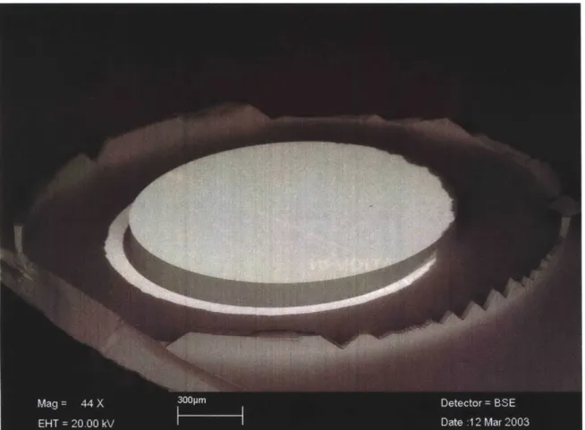
3.3 Fabrication Results
A few of the completed silicon-Pyrex dies have been deliberately broken to
analyze the quality of the silicon and Pyrex surfaces at the valveland. The instruments used for this task are the scanning electron microscope (SEM) and the whitelight profilometer.
Figure 8 is a profilometer scan of the silicon surface measuring the roughness variations. It can be seen that less than 5nm peak-to-peak surface roughness has been preserved on the valveland surface. Figure 9 shows a SEM micrograph of the silicon diaphragm after the fulcrum has been deliberately is broken. When the silicon diaphragm is broken from the Pyrex diaphragm, almost a full ring of the fulcrum remained bonded to the Pyrex. This means the anodic bond is actually stronger than the fulcrum itself.
Figure 8: Profilometer scan of the silicon valveland showing 2nm rms surface roughness.
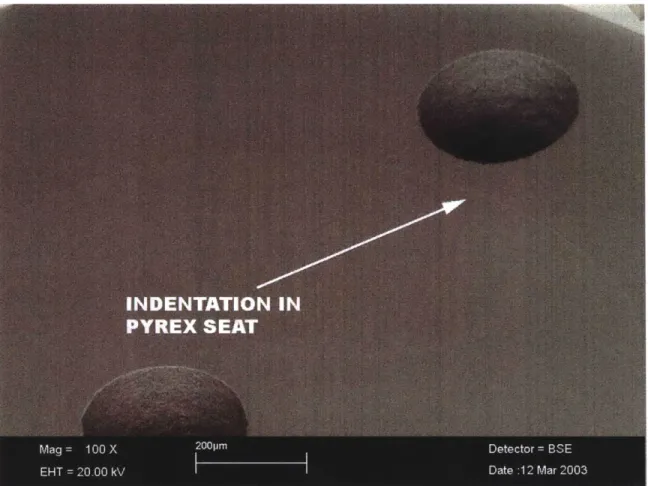
Figure 10 is a profilometer scan of the Pyrex surface after the silicon diaphragm is removed. The ring protrusion is an indentation made by the silicon valveland during the anodic bonding. The thermal cycle of the anodic bond brings the Pyrex wafer to a temperature where it reflows and conforms to the shape of the silicon diaphragm. This is an favorable result since the Pyrex wafer has inherently worse surface roughness than silicon, but the anodic bonding process can modify the Pyrex surface to produce mating silicon and Pyrex surfaces. Figure 11 shows a similar result as Figure 10 in a SEM micrograph.
Figure 9: SEM Micrograph of the silicon diaphragm after the fulcrum is deliberately broken from the anodic bond with the Pyrex wafer
Figure 10: Profilometer scan of the Pyrex wafer after bonding. The reflow of the Pyrex wafer can be seen conforming to the shape of the silicon valveland. The remains of the
Figure 11: SEM of the Pyrex surface after bonding. The faint circle shows the indentation made by the silicon during the anodic bonding process.
4 Circuit Design
This chapter describes the electronic circuits associated with the capacitive measurement system's readout electronics. The analog front-end that converts capacitance to a voltage is described in Section 4.1, followed by the data acquisition system used to digitize the signal in Section 4.2. Finally, the physical implementations of these two subsystems are discussed in Section 4.3. Full schematics, printed circuit board layout, and accompanying software programs are included in the appendices.
4.1 Capacitive Sensing Front-end
The analog front-end converts capacitance to a voltage by exciting the Nanogate capacitor using an AC signal and using analog electronics to measure the electrical response to the signal. The circuitry for this task can be separated into three stages: an input amplifier to buffer the signal from the capacitor, a synchronous detector to mix the signal to DC, and an output filter to remove the out-of-band noise and to shift the output voltage to within range of the ADC (Figure 12) [18].
AD630
10
kHz C1 P LPF SineHP
-,
'4
-
-
+
ADC Input - -Amplifier Sync SignalFigure 12: Capacitive sensing front-end
4.1.1 Input Amplifier
The purpose of the input amplifier is to measure the impedance of the Nanogate capacitor C1 with the least amount of signal degradation caused by parasitic capacitance,
parasitic resistance, and noise. Parasitic capacitance attenuates the response to the measured capacitance and is mainly found between the capacitive sensing electrode and the printed circuit board (PCB), as well as between the input pin and other pins of the amplifier. Modeled as parallel to the capacitor of interest, the parasitic capacitance reduces the measured signal and may vary with time, temperature, and humidity. Parasitic capacitance can be minimized by using guard electrodes around the input that are bootstrapped to the input voltage (dotted lines in Figure 13). Parasitic resistance refers to the leakage current through the input of the amplifier. Its effects on the signal are similar to those of parasitic capacitance. In addition to the use of guard electrodes, parasitic resistance can be minimized by thoroughly cleaning the PCB using flux remover
and by choosing amplifiers that are specifically designed for low input bias current.
CnanoCtte
High Impedance Low Impedance
Non-Inverting Configuration Inverting Configuration
Figure 13: Input amplifier in high and low impedance configuration
There are two fundamental circuit topologies for detecting signal from a capacitive sensor: using a high impedance input to measure voltage and using a low impedance input to measure current (Figure 13). In the high impedance (non-inverting) case, the Nanogate capacitor is a part of a capacitive divider, and the input of the
amplifier moves with the voltage of the signal. In the low impedance (inverting) case, the input of the amplifier is at a virtual ground and a reference capacitor is used in feedback; the capacitively coupled current is converted into a voltage by a transimpedance amplifier. The low impedance configuration is chosen over the high impedance configuration because the full excitation signal can be applied to the Nanogate capacitor compared to only half in the high impedance configuration. Additionally, since the input
of the amplifier is a virtual ground in the low impedance configuration, the operating point of the amplifier is constant, and therefore less prone to common-mode errors.
The OPA129 [23] operational amplifier is chosen as the input amplifier because it offers extremely low input bias current of 100fA maximum. Its minimum unity-gain bandwidth is 0.7MHz, which provides a loop gain of 70 at 10kHz excitation. The input-referred noise at 1OkHz is specified at 15nV/(Hz)-/' voltage noise and 0.1fA/(Hz)-' current noise.
The input amplifier circuit is shown in Figure 14. C1 is the Nanogate capacitor, and C2 is a reference capacitor of approximately the same value as C1. R1, R2, and R3 form a resistive T-network to provide a high impedance DC path to ensure that the inverting input does not float to arbitrary voltages.
V C 1
-ut = 1 iffexcitation >> , (3)
Vi, C2 2rR#C
where Rf is the equivalent parallel resistance to C2. The T-network formed by R1,
R2, and R3 reduces the feedback to the input by the ratio of R2/R3 and, consequently,
magnifies the effective parallel resistance to C2 by the same factor. An effective parallel
resistance of 500MQ is achievable, far beyond the value that can be realized using conventional components. The resulting time constant of the feedback loop is approximately 100Hz, which satisfies the condition of equation 3 for a fexcittion of 10kHz.
The disadvantage of the T-network is that the offset of the input amplifier is also multiplied by the same ratio as the feedback resistance. Therefore, output of the input amplifier is AC coupled to the next stage to eliminate errors caused by offset drift.
C2 R1 R2 R3 C1 Vout 10 k Cstray P 1 29
4.1.2 Synchronous Detector
Synchronous detection is a signal conditioning technique designed to detect the amplitude of a fixed-frequency signal in the presence of noise. In this scheme the measured signal is multiplied with a reference signal of the same frequency and phase. The amplitude of the desired signal is therefore transformed down to DC, while low frequency noise is transformed up to the reference frequency. The output of the multiplier can then be low-pass filtered to remove the noise at the reference frequency and beyond.
The multiplier that follows the input amplifier is the AD630 precision modulator from Analog Devices [24]. The AD630 has two parallel amplifiers with gains of +1 and -1, and switches the output between the two amplifiers at the frequency of the reference signal. This has the effect of multiplying the input signal with a square wave at the reference frequency, and it is insensitive to amplitude of the reference signal. Figure 12 shows the simplified schematic of the AD630 where the input signal is the output of the
OPA129 and the reference signal comes from a TTL gate derived from the 10kHz
sinusoidal source.
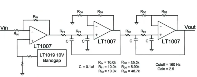
4.1.3 Output Signal Conditioning
The output of the AD630 is level shifted and low-pass filtered before being digitized by an ADC. The level shift moves the DC level of the output to a voltage range acceptable for the ADC, and is implemented using a LT1007 operational amplifier [25] in an inverting configuration with unity gain (Figure 15). The amount of shift is determined
by the voltage at the non-inverting terminal, which is set by a LT 1019 bandgap reference [26] followed by a voltage divider.
The low-pass filter removes out-of-band signals from synchronous detection and sets the total system bandwidth. A four-pole voltage-controlled voltage-source (VCVS) filter is implemented using two LT1007 operational amplifiers (Figure 15) [27, 28]. This filter has a bandwidth of 160 Hz and a total gain of 2.5.
RDO RD2
Figure 15: Level shifter and 4-pole VCVS low-pass filter
4.1.4 Switched Calibration
The long-term variation in the offset of the AD630 and the output stage is calibrated using a switched reference source at the input of the AD630 (Figure 16). At periodic instances a reference signal is switched into the AD630 and its result is stored and used as the overall system offset. The reference signal is generated using an identical
OPA129 input amplifier where the Nanogate has been replaced by a reference capacitor.
The switch is implemented using an AD45 1, a low on-resistance analog switch.
Input
AD451
10
c
AmplifierAD630
ADC
Reference Amplifier
Calibration Signal Sync Signal
Figure 16: Switched calibration circuit
4.2 Data Acquisition System
A custom data acquisition system is designed to digitize the output of the analog
section. The three main components of this system include a high resolution ADC, a
microprocessor, and a computer. A temperature sensor is also included to measure signal drift as a function of temperature. The analog input is digitized by the ADC and read by the microprocessor, which also measures input from the temperature sensor and controls the Nanogate's external actuator. The capacitance and temperature data from the microprocessor and the displacement data from the Zygo interferometer are logged by a Visual Basic program on the computer.
From Zygo Interferometer
Analog
Differential
Input MSP430Computer:
--
ADClMicroprocessor
RS232Vu aicProgram Intemnal ADC
TemperatureToAtar
Sensor
Figure 17: Data Acquisition System
4.2.1 Analog to Digital Conversion
Voltage output from the analog front-end is digitized using a LTC2440 ADC from
Linear Technology [29]. The LTC2440 is a differential input with a 2.5V range and 24 bits digital output. The maximum sampling rate is 4 kilo-samples-per-second (ksps) but is settable to allow the user to exchange resolution for bandwidth. On this particular data
acquisition board, the LTC2440 is set to sample at 1 ksps, which corresponds to an
effective resolution of 114 dB, significantly more than the required 74 dB.
4.2.2 MSP430 Microprocessor
The functions of the microprocessor include reading data from the ADC, measuring temperature, controlling the Nanogate's external actuator, and relaying data to the computer. The MSP430 microprocessor series from Texas Instruments is chosen because of its programmability. Specifically, the MSP430F149 [30] is used. It has 60 kilobytes of flash program memory, an internal 12-bit ADC, 2 timers, and can be clocked
up to 8MHz. The microprocessor communicates with the ADC over a 3-wire SPI interface.
The temperature is measured using an AD592 temperature dependent current source [31]. The AD592 sources current proportional to absolute temperature at a ratio of 1 uA/K. The output current is converted to voltage via a resistor and digitized using the MSP43O's 12-bit internal ADC. The measured temperature resolution is 0.125'C.
The Nanogate actuator is controlled via several digital lines provided by the MSP430. These signals include clock, step command, and direction. Since the actuator takes in 5V TTL signals and the MSP430 runs at 3.3V, a Schmidt-triggered inverter is used as an interface.
The MSP430 communicates with the computer via a serial line at 57.6 kbits/s. The internal UART of the MSP430 is connected to a RS-232 line driver, which is connected to a computer using a standard 9-pin serial connector.
4.2.3 Visual Basic Data Logger and User Interface
Capacitance, temperature, and displacement from the Zygo interferometer are read by a Visual Basic program (Figure 18), which stores the data on disk and provides a real-time stripchart display. This program is also allows the user to send commands to control the external actuator via the microprocessor. The actuator motion can be controlled by single commands or a script that automatically performs motion (up, down, and wait) sequences.
4.3 Physical Circuit Considerations
4.3.1 Electrical Contact to Capacitive Electrodes
The capacitive electrodes on the silicon and Pyrex part of Nanogate are connected to the analog front-end via thin, flexible copper wires (Figure 19). The wires are bonded
by conductive epoxy [32] to the electrodes on the Nanogate and are soldered to pads on
the printed circuit board. The wires are single strands taken from standard 26 gauge stranded wire.
Figure 19: Electrical connection between capacitive electrodes and input amplifier
4.3.2 Printed Circuit Board Design and Layout
The analog front-end and data acquisition circuits are implemented on standard 2-layer, 62 mil, FR-4 printed circuit boards (PCB). The two circuits are made on separate boards in order to minimize interference between the two circuits and to modularize the development effort. The signal lines between the two PCBs are connected via SMA-type
coaxial cable, which provide a shielded electrical connection with a flexible mechanical connection.
Ground planes are used extensively on the two PCBs to reduce the interference caused by external electromagnetic fields. All components are placed on the top of the circuit board so that a complete ground plane can be formed on the bottom side of the PCB. The data acquisition PCB has separate ground planes between the ADC and the microprocessor section of the board in order to reduce the effect of digital noise on the
ADC. The two PCBs are also enclosed in a grounded metal box for shielding against
external interference signals.
Power on the two circuit boards are supplied via several voltage regulators to minimize the interference coupled through the power supply. The analog front-end is supplied +12V and -12V rails for its analog components. A dedicated 5V digital rail is provided for the logic supply on the analog switch. The data acquisition circuit board is powered with a 5V analog line for the LT2440 ADC and temperature sensor, a 5V digital line for driving the picomotor actuator, a 3.3V analog rail for the ADC onboard the microprocessor, and a 3.3V digital rail for digital functions on the microprocessor.
The placement of components and signal lines on the circuit board is also given careful consideration. Every effort is made to keep the length of signal lines as short as possible and components that can add noise to the signal line, such as digital logic gates,
are deliberately placed farther away.
After the components are soldered onto the board, the PCBs are cleaned extensively with flux-remover to clear away the leftover flux residue. Since the DC impedances on the circuit board range from 10-500 MQ, the electrical conduction of flux can be a significant parasitic.
Figure 20 and Figure 21 are photographs of the analog front-end and data acquisition PCBs. The detailed schematic and PCB layout are shown in Appendix C.
Figure 20: Photograph of the analog front-end PCB
Figure 21: Photograph of the data acquisition PCB showing split ground planes for the
5
Results and Discussion
This chapter presents the results from testing the capacitive displacement sensor. Section 5.1 describes the results of the capacitance versus displacement measurement. Section 5.2 analyzes the noise floor of the capacitance measurement. Finally, section 5.3 examines the drift error of the capacitance measurement.
5.1 Capacitance versus Displacement
As discussed in section 2.3, each Nanogate device needs to be calibrated using the Zygo interferometer. As external deflection is applied to the silicon diaphragm, the data acquisition software records the value of the ADC from the capacitive measurement circuit, displacement as measured by the Zygo interferometer, and the room temperature. In order to minimize drift in the Zygo readings caused by air currents, the laser beam is shielded using acrylic tubes. Figure 22 shows the sequence of actuator deflections, Figure
23 shows the response of the capacitive sensor, and Figure 24 shows the response of the
Zygo interferometer. The droop of the capacitance and Zygo output after each set of input steps is an artifact of the actuator assembly: The force on the silicon diaphragm is applied through an o-ring, which has a relatively slow relaxation time.
Figure 25 shows the calibration of Zygo measured displacement versus capacitance. This graph has three distinct regions. In region I, the capacitance is increasing in response to the deflection from the actuator while the central valveland remains fixed. This is because the deflection of the outer edge must first overcome the preload due to the additional thickness of the metal film layer that causes the diaphragm to bend during the anodic bonding. Region III shows the valveland displacement varying as a linear function of capacitance as in equation (2). Region II is the non-linear, transition between regions I and III. It is hypothesized that this transition region is caused
by asymmetry in the actuation of the outer edge of the silicon diaphragm and with better
actuation schemes the rounded region can be reduced. The roundedness of this region makes it difficult to define a zero point. It is possible to interpolate this point by fitting a
Figure 26 shows the Zygo versus capacitance plot subtracted from its linear fit line in region III of Figure 25. A periodic fine structure, on the order of 5nm, is revealed
and consistent during both the opening and the closing of the Nanogate. The source of this behavior is likely an artifact of the actuator and how it interacts with the mounting structure, however, more analysis is necessary to fully understand this problem.
Actuator versus time (file:log1.004)
3000 2500- 2000-E$ 1500-a) 2 1000-0 E 0 o 0-10 20 30 40 50 60 70 80 Time (s)
Figure 22: Actuator command versus time
-500-
-1000--1500
Capacitance versus time (file:logl.004)
0 10 20 30 40 50 60 70 80
Time (s)
Figure 23: Capacitance output in ADC counts versus time
Zygo raw data (file:logl.004)
40
Time (s)
Zygo vs. Capacitance (file;logl.004)
N
7.8 8 8.2 8.4 8.8 8.8 9
Capacitance (ADC counts) x 108
Figure 26: Residue plot of Zygo vs. Capacitance minus its linear fit line in region III of Figure 25
Capacitance (ADC counts)
x10"Figure 25: Zygo vs. Capacitance divided into 3 regions