HAL Id: hal-00002689
https://hal.archives-ouvertes.fr/hal-00002689
Preprint submitted on 24 Aug 2004
HAL is a multi-disciplinary open access
archive for the deposit and dissemination of
sci-entific research documents, whether they are
pub-lished or not. The documents may come from
teaching and research institutions in France or
abroad, or from public or private research centers.
L’archive ouverte pluridisciplinaire HAL, est
destinée au dépôt et à la diffusion de documents
scientifiques de niveau recherche, publiés ou non,
émanant des établissements d’enseignement et de
recherche français ou étrangers, des laboratoires
publics ou privés.
Dependence of the superconducting transition
temperature on the doping level in single crystalline
diamond films.
Etienne Bustarret, Jozef Kacmarcik, C. Marcenat, Etienne Gheeraert,
Catherine Cytermann, Jacques Marcus, Thierry Klein
To cite this version:
Etienne Bustarret, Jozef Kacmarcik, C. Marcenat, Etienne Gheeraert, Catherine Cytermann, et al..
Dependence of the superconducting transition temperature on the doping level in single crystalline
diamond films.. 2004. �hal-00002689�
E. Bustarret1, J. Kaˇcmarˇcik2,3, C. Marcenat3 , E. Gheeraert1, C. Cytermann4, J. Marcus1 and T. Klein1,5
1 Laboratoire d’Etudes des Propri´et´es Electroniques des Solides,
CNRS, B.P.166, 38042 Grenoble Cedex 9, France
2
Centre of Low Temperature Physics IEP SAS & FS UPJ ˇS, Watsonova 47, 043 53 Koˇsice, Slovakia
3 Commissariat `a l’Energie Atomique - Grenoble,
D´epartement de Recherche Fondamentale sur la Mati`ere Condens´ee, SPSMS, 17 rue des Martyrs, 38054 Grenoble Cedex 9, France
4 Physics Department and Solid State Institute, Technion, 32000 Haifa, Israel and 5
Institut Universitaire de France and Universit´e Joseph Fourier, B.P.53, 38041 Grenoble Cedex 9, France (Dated: August 5, 2004)
Homoepitaxial diamond layers doped with boron in the 1020− 1021cm−3
range are shown to be type II superconductors with sharp transitions (∼ 0.2 K) at temperatures increasing from 0 to 2.1 K with boron contents. The critical concentration for the onset of superconductivity is about 5 − 7 1020 cm−3
, close to the metal-insulator transition. The H − T phase diagram has been obtained from transport and a.c. susceptibility measurements down to 300 mK. These results bring new quantitative constraints on the theoretical models proposed for superconductivity in diamond.
PACS numbers: 74.25.Op, 74.63.c, 73.61.Cw
Type II superconductivity has been recently reported for heavily boron-doped polycrystalline diamond pre-pared either as bulk [1] or thin film samples [2], provid-ing a new interestprovid-ing system for the study of supercon-ductivity in doped semiconductors. Based on the great bonding strength of the valence band states and on their strong coupling to the carbon lattice phonons, various theoretical studies [3, 4] have stressed the similarity be-tween diamond and the recently discovered MgB2system
which shows a surprizingly high Tc value on the order of
40 K. Those calculations lead to Tc values in the 0.2 to
25 K range (depending on the boron content) but ignore the boron impurity band [3, 4]. An alternative theo-retical approach [5] stresses out the fact that the boron concentration range where superconductivity has been observed is close to the Anderson-Mott metal-insulator transition and suggests an electron correlation driven ex-tended s−wave superconductivity in the boron impurity band.
The open questions of the nature of the metal-insulator transition (MIT) in diamond and of its correlation with superconductivity are of fundamental interest and pro-vide ample motivation for this first investigation of the dependence of the superconducting transition tempera-ture on the doping boron concentration. In this letter, we report on magnetic and transport experiments on a set of high quality single crystalline epilayers doped in the rel-evant 1020− 1021 cm−3 range. We show that T
c rapidly
increases above some critical concentration ∼ 5 − 7 1020
cm−3 reaching ∼ 2 K for nB = 19 1020 cm−3 (see Table
1).
001-oriented type Ib diamond substrates were first ex-posed to a pure hydrogen plasma. Methane (4%) was subsequently introduced and a 0.5µm-thick buffer layer of non-intentionally doped material was deposited at 820◦ C by the microwave plasma-assisted decomposition
TABLE I: Sample characteristics : thickness (t), gas phase ratio ((B/C)gas), boron concentration (nB) and critical
tem-peratures (Tc) for the studied diamond epitaxial films
Sample t (µm) (B/C)gas (ppm) nB (1020cm−3) Tc (K) 1 3.0 1615 3.6 ≤ 0.05 2 3.0 1730 9 0.9 3 3.0 1845 10 1.2 4 2.0 2200 11.5 1.4 5 0.15 2800 19 2.1
(MPCVD) of the gas mixture at a total pressure of 30 Torr. Finally, diborane was introduced in the vertical silica wall reactor with boron to carbon concentration ratios in the gas phase ((B/C)gas)ranging from 1500 to
3000 ppm. With a typical growth rate of 0.9µm/hr these deposition conditions led to 0.1 to 4µm-thick p+−type
di-amond layers. Secondary Ion Mass Spectroscopy (SIMS) depth profiles of 11B−, 12C− and 11B12C− ions were
measured using a Cs+ primary ion beam in a Cameca
Ims 4f apparatus. As shown in Fig.1 for samples 2, 4 and 5, these profiles were found to be flat or with a slow decrease toward the buffer layer. The boron atomic den-sities nB shown both in Fig.1 and Table 1 were derived
from a quantitative comparison to a SIMS profile mea-sured under the same conditions in a B−implanted di-amond crystal with a known peak boron concentration of 2.4 1020 cm−3. For thin enough samples, the profile
yielded also the residual doping level in the buffer layer, around 1018 cm−3. Moreover, the single crystal and
epi-taxial character of the MPCVD layers was checked by high resolution X-ray diffraction, yielding shifted narrow lines with smaller linewidths at half maximum than for the Ib substrate (typically 10 arcsec for the 004 Bragg spot of the epilayer, instead of 13 arcsec for the
sub-2 1018 1019 1020 1021 0 50 100 150 200 250
Boron atomic concentration (cm
-3 ) Sputtered depth (nm) #2 #5 sputtering stop #4 12C11B- (m = 23) buffer
FIG. 1: SIMS profiles for ion mass 23 obtained using Cs+
primary ions on samples 2, 4 and 5. In the case of the thicker samples, sputtering was interrupted before reaching the buffer layer.
strate). The chemical composition [6], structural [7, 8] and optical [6, 8, 9] characteristics of these layers at room temperature are well documented and have been reviewed recently, together with some preliminary trans-port measurements [8].
The superconducting temperatures have been deduced from ac-susceptibility measurements (χac). The films
have been placed on top of miniature coils and Tc has
been obtained by detecting the change in the self induc-tion of the coils induced by the superconducting tran-sitions. For fully screening samples, we observed a 4% drop of the induction L (∼ 1 mH). Small ac-excitation fields (ω ∼ 99 kHz and hac∼ a few mG) have been
ap-plied perpendicularly to the films. Four Au/Ti electrodes were deposited on top of the film with the highest Tc for
magneto-transport measurements. A very small current (∼ 1nA) corresponding to a current density on the order of 10−3 Acm−2 has been used to avoid flux flow dissipa-tion. A standard lock-in technique at 17 Hz was used to measure the temperature dependencies of the sample re-sistance at fixed magnetic fields. The measurements were performed down to 50 mK (χac) and 300mK (transport)
and the magnetic field was applied perpendicularly to the doped plane of the sample,
The critical temperatures (see Table 1) reported in Fig.2 have been deduced from the onset of the diamag-netic signal (see inset of Fig.2). The susceptibility has been rescaled to −1 in the superconducting state and a N ∼ 0.9 demagnetization coefficient has been used (the values of Tc do not depend on this choice). This choice
for N leads to a dissipation peak on the order of 0.2 − 0.3 as expected for the non linear regime. This is consistent with the observation of a slight increase of the width
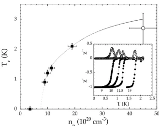
0 1 2 3 0 10 20 30 40 50 T c (K) n B (10 20 cm-3) -1 -0.5 0 0.5 0 0.5 1 1.5 2 2.5 χ ' χ '' T (K) 9 10 11.5 19
FIG. 2: Dependence of the superconducting transition tem-perature Tcon the boron concentration nB : closed squares :
this work, open circle : from [1].The different Tcvalues were
obtained from the onset of the diamagnetic signal (see inset for the real (closed symbols) and imaginary (open symbols) parts of the magnetic susceptibility.
of the transition for increasing hac values. As shown in
the inset of Fig.2 (and Fig.3), the transitions are very sharp (with a width ∼ 0.2 K) allowing an accurate de-termination of Tc and stressing out the high quality of
our samples. In comparison, the polycrystalline samples measured in previous reports presented a much larger re-sistivity transition width, ∼ 1.7 K in [1] and ∼ 2.6 K in [2].
No transition was observed down to 50 mK for the film with nB = 3.6 1020 cm−3. For higher boron
concentra-tions, Tc increases rapidly with doping above some
crit-ical concentration ∼ 5 − 7 1020 cm−3 reaching 2.1 K for nB = 19 1020 at.cm−3. The dependance of Tc with
dop-ing extrapolates towards the data recently obtained by [1]. On the contrary, our Tc value for nB ∼ 1021 cm−3
(∼ 1 K) is much lower than the one recently reported by [2] (∼ 4 − 7 K). Our data suggests that these au-thors have largely underestimated the boron concentra-tion of their polycrystalline samples. They deduced this concentration from Hall measurements which are known to give results that deviate significantly from the actual boron concentration in p+−type diamond [7]. It is also
worth noticing that we observed superconducting tran-sitions with Tc on the order of 1 K for boron contents
∼ 0.5at.% whereas recent calculations of the electron-phonon coupling led to much smaller Tc values for these
doping levels [3–5].
The influence of an external field on the superconduct-ing transition is displayed in Fig.3. As shown in panel a, the transition is shifted towards lower temperatures as the magnetic field is increased. The transition width
re--1 -0.8 -0.6 -0.4 -0.2 0 0 0.2 0.4 0.6 0.8 1
χ
'
T(K) 0.7T 0.5T 0.3T 0 T 0.1T (b) n = 9.1020 cm-3 0 5 10 15 20 25 30 35 0.5 1 1.5 2 2.5 R ( Ω ) T (K) 1.4T 1.2T 1.0T 0.8T 0.6T 0.4T 0.2T 0T (a) n = 19.1020 cm-3FIG. 3: (a) : temperateure dependence of the electrical re-sistance at indicated magnetic fields for the film with n = 19.1020 at.cm−3. The dashed lines correspond to the two criteria used for the determination of Hc2 (see Fig.3) i.e.
R/RN = 90% and 10% (RN being the normal state
resis-tance).(b) temperature dependence of the real part of the magnetic susceptibility at indicated magnetic fields for the film with n = 9.1020 at.cm−3
. Hc2 has been deduced from
the onset of the diamagnetic signal.
mains relatively small up to ∼ 1 T and rapidly increases for larger fields. In the absence of thermodynamic mea-surements, some care should be taken in order to define an accurate Hc2line. This line has been defined from the
classical R/Rn = 90% criterion (where RN is the normal
state resistance). As shown in Fig.4, the corresponding Hc2(T ) line can be well described by the classical WHH
theory [10]. We hence get Hc2(0) ∼ 1.4 T
correspond-ing to a coherence length ξ0 = pΦ0/2πHc2(0) ∼ 150˚A
for nB = 19 1020 cm−3 (Φ0 being the flux quantum).
We have also reported on Fig.4 the line corresponding to R/Rn= 10% which gives an indication for the width
0 0.2 0.4 0.6 0.8 1 1.2 1.4 1.6 0 0.5 1 1.5 2 2.5 H c2 (T) T (K) 19 1020 cm-3 9 1020 cm-3
FIG. 4: H − T phase diagram for the films with nB= 19 1020
cm−3 and nB = 9 1020 cm−3. The circles (resp. diamonds)
have being deduced from temperature sweeps of the electrical resistance (see fig.2) for R/Rn= 90% (resp. R/RN= 10%).
The shadowed area is an indication of the width of the tran-sition. The closed squares were defined from the onset of the ac-susceptibility (see Fig.2(b)). The full lines are fits to the data using the classical WHH theory.
of the transition, pointing out that the transition curves rapidly increase for H > 1 T. For sample 2, this line has been deduced from the shift of the diamagnetic response with increasing fields. In this case, the rapid broadening of the transition is the hallmark of a small critical cur-rent density (Jc) again emphasizing the high quality of
our films. Indeed, in the non linear regime, the suscepti-bility is directly related to Jcd/hac(where d is a
charac-teristic length scale on the order of the sample thickness) and Jc ≈ hac/d ∼ 1 Acm−2 for χ0 ∼ −0.4. In this case,
no saturation was observed down to 200 mK, indicating some deviation from the classical WHH behaviour. Note that for both samples the slope [dHc2/dT ]T →0∼ 1 T/K,
which is almost 2 times smaller than the value reported by Ekimov et al. [1].
We obtained an almost temperature-independent nor-mal state resistivity on the order of 0.5 mΩ.cm for nB =
19 1020cm−3suggesting that our samples are close to the
metal-insulator transition. On the basis of the criterion first proposed by Mott [11] for metal-non metal transi-tions, which in its final form (Nc1/3aH = 0.26, where
aH is the Bohr radius) has been verified in a wide
vari-ety of condensed media [12], the critical concentration in p−type diamond is expected to be around Nc = 1−2 1020
cm−3 [13]. Limitations to this approach arise from the discrepancies in the values proposed in the literature for
4 the acceptor Bohr radius aH, in line with other
inconsis-tencies about the valence band parameters of diamond. From an experimental point of view, extrapolations [14] of the Pearson-Bardeen model [15] have led to Nc
val-ues ranging from 1.5 to 3.0 1020 cm−3, while different
transport measurements have prompted other authors to propose that Nc∼ 7 1020cm−3 [16]. It is worth noticing
that those values have been deduced from room temper-ature measurements. To the best of our knowledge, the only low temperature estimate (Nc∼ 40 1020cm−3) has
been proposed by Tschepe et al. [17] on the basis of a scaling analysis of the electrical conductivity. How-ever, the absolute conductivity values of their implanted samples are much lower than ours despite larger boron concentrations.
The proximity of a MIT in this system, makes it very favorable for the observation of quantum fluctua-tion effects. The strength of these fluctuafluctua-tions can be quantified through the quantity Qu = Ref f/RQ where
RQ = ~/e2 ∼ 4.1 kΩ is the quantum resistance and
Ref f = ρN/s (s is a relevant length scale for these
fluc-tuations [18]). Taking ρN ∼ 5 10−4Ω.cm and s ∼ ξ(0) ∼
150˚A, we obtain a large Qu ratio ∼ 0.1 indicating that
quantum effects may be important in this system. These quantum fluctuations may give rise to the melting of the flux line lattice and thus lead to the rapid broadening of the resitive transitions observed at low T and large H. Another indication for such quantum effects, is the almost temperature-independent mixed state resistivity above 1.2 T as previously observed in other systems with similar Quvalues [19, 20]
To conclude, we were able to prepare highly homoge-neous and well characterized boron-doped diamond films in the 1020 - 1021 cm−3 range where superconductivity occurs. The value of the critical concentration for the onset of superconductivity is on the order of 5 − 7 1020
cm−3. Boron-doped diamond is an ideal system to study the occurence of superconductivity close to the metal-insulator transition. As a consequence, quantum effects are expected to play a significant role as suggested by the large quantum resistance ratio Qu∼ 0.1.
We are grateful to F. Pruvost who grew some of the diamond layers and to Dr L. Ortega (Cristallographie, CNRS, Grenoble) for the X-ray diffraction experiments.
[1] E.A. Ekimov, V.A. Sidorov, E.D. Bauer, N.N. Melnik, N.J. Curro, J.D. Thompson, S.M. Stishov, Nature 428 542 (2004).
[2] Y. Takano, M. Nagao, K. Kobayashi, H. Umezawa, I. Sakaguchi, M. Tachiki, T. Hatano, H. Kawarada, cond-mat.0406053.
[3] L. Boeri, J. Kortus, O.K. Andersen, cond-mat.0404447. [4] K.W. Lee, W.E. Pickett, cond-mat.0404547.
[5] G. Baskaran, cond-mat.0404286.
[6] E. Bustarret, F. Pruvost, M. Bernard, C. Cytermann, C. Uzan-Saguy, phys. stat. sol. (a) 186 203 (2001).
[7] E. Bustarret, E. Gheeraert, K. Watanabe, phys. stat. sol. (a) 199 9 (2003).
[8] F. Brunet, P. Germi, M. Pernet, A. Deneuville, E. Gheer-aert, F. Laugier, M. Burdin, G. Rolland, Diam. and Re-lat. Mater. 7 869 (1998).
[9] F. Pruvost, E. Bustarret, A. Deneuville, Diam. and Rel. Mater. 9 295 (2000).
[10] N.R.Werthamer, E.Helfand and P.C.Hohenberg Phys. Rev. 147 295 (1966).
[11] N.F. Mott, Can. J. Phys. 34 1356 (1956).
[12] P.P. Edwards and M.J. Sienko, Phys. Rev. B 17 2575 (1978).
[13] H. Shiomi, Y. Nishibayashi, N. Fujimori, Jpn J. Appl. Phys. 30 1363 (1991); A. S. W. Williams, E. C. Lightowlers, A.T. Collins, J. Phys. C 3 1727 (1970). [14] T.H. Borst, O. Weis, Diam. Relat. Mater. 4 848 (1995);
J.-P. Lagrange, A. Deneuville, E. Gheeraert, Diam. Re-lat. Mater. 7 1390 (1998).
[15] G.L. Pearson and J. Bardeen, Phys. Rev. B 17 2575 (1978).
[16] K. Nishimura, K. Das, J.T. Glass, J. Appl. Phys. 69 3142 (1991).
[17] T. Tschepe, J.F. Prins, M.J.R. Hoch, Diam. Relat. Mater. 8 1508 (1999).
[18] G.Blatter, B.Ivlev, Y.Kagan, M.Theunissen, Y.Volokitin and P.Kes, Phys. Rev. B 50 13013 (1994).
[19] A.Yazdani and A.Kapitulnik, Phys. Rev. Lett. 74 3037 (1995).
[20] S.Okuma, Y.Imamoto and M.Morita, Phys. Rev. Lett. 86 3136 (2001).