Copper Wafer Bonding in Three-Dimensional Integration
byKuan-Neng Chen
B. S., National Cheng Kung University (1996) M. S., National Tsing Hua University (1998)
Submitted to the Department of Electrical Engineering and Computer Science in partial fulfillment of the requirements for the degree of
Doctor of Philosophy
at the MASSACHUSETTS INS E
OF TECHNOLOGY
MASSACHUSETTS INSTITUTE OF TECHNOLOGY MAR 14
2005
January 2005
LIBRARIES
C Massachusetts Institute of Technology 2005. All rights reserved.
BARKER
A uthor... ...
Department of Electrical Enginieering and Computer Science December 27, 2004
Certified by... ... ...
Rafael Reif Departmental Head and Professor of Electrical Engineering and Computer Science Thesis Supervisor
A ccepted by ... ...
Arthur C. Smith Chairman, Departmental Committee on Graduate Students Department of Electrical Engineering and Computer Science
Copper Wafer Bonding in Three-Dimensional Integration
Kuan-Neng Chen
Submitted to the Department of Electrical Engineering and Computer Science On December 27, 2004, in partial fulfillment of the
Requirements for the degree of Doctor of Philosophy Abstract
Three-dimensional (3D) integration, in which multiple layers of devices are stacked with high density of interconnects between the layers, offers solutions for problems when the critical dimensions in integrated circuits keep shrinking. Copper wafer bonding has been considered as a strong candidate for fabrication of three-dimensional integrated circuits
(3-D IC). This thesis work involves fundamental studies of copper wafer bonding and
bonding performance of bonded interconnects.
Copper bonded wafers exhibit good bonding qualities and present no original bonding interfaces when the bonding process occurs at 400'C/4000 mbar for 30 min, followed by nitrogen anneal at 400'C for 30 min. Oxide distribution in the bonded layer is uniform and sparse. Evolution of microstructure morphologies and grain orientations of copper bonded wafers during bonding and annealing were studied. The bonded layer reaches steady state after post-bonding anneal. The microstructure morphologies and bond strengths of copper bonded wafers under different bonding conditions were investigated. A map summarizing these results provides a useful reference on process conditions suitable for three-dimensional integration based on copper wafer bonding.
Similar microstructure morphology of copper bonded interconnects was observed to that of copper bonded wafers. Specific contact resistances of bonded interconnects of
approximately 10-8 Q-cm2 were measured by using a novel test structure which can
eliminate the errors from misalignment during bonding. The bonding qualities of different interconnect sizes and densities have been investigated. In addition to increasing the bonding temperature and duration, options such as larger interconnect sizes, total bonding area, or use of dummy pads for bonding in the unused area improve the quality
Process development of silicon layer stacking based on Cu wafer bonding was successfully applied to demonstrate a strong four-layer-stack structure. Bonded Cu layers in this structure become homogeneous layers and do not show original bonding interfaces. This process can be reliably applied in three-dimensional integration applications.
Thesis Supervisor: Rafael Reif
Acknowledgments
I would like to thank my advisor, Professor Rafael Reif, for providing support for this
research project. From Professor Reif, I received not only research training but also his attitude toward life. His mentorship has been an inspiration to me. I would also like to thank Professors Duane Boning and Clifton Fonstad for participating in my thesis
committee and providing feedback at various stages of this thesis.
I appreciate that Professors Jesus del Alamo, Judy Hoyt, and Franz Partner always
shared their valuable knowledge in their courses and provided academic support for me. In addition, I appreciate the brainstorming done with Professor Caroline Ross and Loma Gibson in the early stage of my thesis.
The research collaboration with Dr. Shu-Ming Chang and Dr. Li-Cheng Shen from Industrial Technology Research Institute in Taiwan was a wonderful experience. Mr. Wen-Cheng Yen offered assistance with the experiments and valuable discussions of my research. The research collaboration with Professor James Meindl's group at Georgia Institute of Technology provided me the opportunity to apply my research in other applications.
I have benefited both academically and socially by interacting with many people
within MIT. I would like to thank my colleagues in Reifgroup, Andy Fan, Chuan Seng Tan, Nisha Checka, Ajay Somani, Tan Mau Wu, Piotr Mitros, and Susan Kaufman for their company and making a pleasant work environment. I also thank other 3D enthusiasts, Andy Fan, Chuan Seng Tan, and Nisha Checka, for their brainstorming
sessions about my research. Andy Fan and Chuan Seng Tan read my manuscripts and provided me useful feedback before submission.
It would have been impossible to finish my thesis without the support and technical discussions from all of the staffs in the MIT Microsystems Technology Laboratories, especially Mr. Kurt Broderick. With his assistance, the use of the bonder machine and other equipments became simple and joyful.
This work has been carried out as part of the Interconnect Focus Center Research Program at the Massachusetts Institute of Technology, and is supported in part by the Microelectronics Advanced Research Corporation (MARCO), its participating companies, and DARPA under contract 2003-IT-674. I would also like to acknowledge the support on one project of my thesis from the International Program Center, ITRI, Taiwan.
This thesis is dedicated to my family, especially my parents, Yin-Mei Liang and Yun-Kai Chen, who constantly give me their unreserved love and support through out my life.
Mostly I would like to thank my wonderful wife I-Ning Lee for her love and support over the years. Thanks to her encouragement, I have had the confidence and energy to overcome difficulties and finish this thesis.
Contents
1 Introduction
19
1.1 M otivation ... 19
1.2 Three-dimensional (3D) Integration... 20
1.3 MIT Three-dimensional Integration... 22
1.4 Wafer Bonding... 26
1.5 Advantages of Using Copper as the Bonding Material... 27
1.6 Research Goal and Contribution of Thesis Work... 29
1.7 Thesis Organization... 30
2 Bonding Process and Description of Experiments 33 2.1 Initial Wafer Preparations... 33
2.2 Thin Film Deposition... 34
2.3 Copper Surface Cleaning... 35
2.4 Optical Wafer-Wafer Alignment... 35
2.5 Bonding Process... 36
2 .6 A nn eal... 36
2.7 Bonding Strength Examinations... 38
2.7.2 Tape Test... 38
2.7.3 Pull Test... . 38
2.7.4 Shear Test... 39
2.8 Scanning Electron Microscope (SEM) Observation... 39
2.9 Transmission Electron Microscope (TEM) Observation... 39
2.9.1 Sample Preparation... 39
2.9.2 Sample Observation... 41
2.10 Energy Dispersion Spectrometer (EDS) Analysis... 41
2.11 Atomic Force Microscope (AFM) Observation... 41
2.12 X-ray Diffraction (XRD) Analysis... 42
2.13 Wafer Bow Measurement... 42
2.14 Electrical Properties Measurement... 42
3 Initial Results of Copper Wafer Bonding 43 3.1 R azor Test... .... 44
3.2 Initial Test R esult... 44
4 Microstructures of Copper Bonded Layer 47 4.1 Sample Preparation and Experimental Procedures... 48
4.2 Interfacial Morphologies... 48
4.2.1 TEM Observation... 48
4.2.2 D iscussion... 50
4.2.3 Types of Morphologies... 53
4 .4 Sum m ary ... 58
5 Evolution of Materials Properties During Bonding Process 59 5.1 Sample Preparation and Experimental Procedures... 60
5.2 Interfacial Morphologies Evolution Observation... 60
5.3 Effects of Bonding and Anneal on Microstructure Evolution... 62
5.4 Grain Size Evolution Observation... 64
5.5 Mechanism of Abnormal Grain Growth during Bonding... 64
5.6 Sum m ary ... .... 67
6 Interfacial Morphology of Bonded Layer under Different Bonding Conditions 69 6.1 Sample Preparation and Experimental Procedures... 70
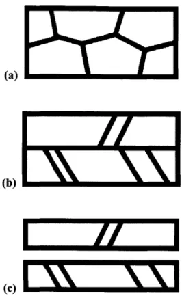
6.2 Categories of Morphologies... 70
6.3 Observation Results... 72
6.4 D iscussion... 75
6.5 Sum m ary ... 78
7 A Map of Bonding Quality and Bonding Strength Investigation Using Different Test Techniques 80 7.1 Test Bonded Sample Preparation... 80
7.2 D icing Test... 80
7.3 The Effect of Anneal Temperature on Bonding Quality... 82
7.5 Tape T est... 84
7.6 Pull Test... . .... 87
7.7 Shear Test... 90
7.8 Sum m ary ... .... 93
8 Effects of Wafer Bow on Bonding Quality 95 8.1 Sample Preparation and Experimental Procedures... 96
8.2 Wafer Bow Evolution During the Heating Process... 97
8.3 Wafer Bow and Bonding Quality at Different Bonding Temperatures... 98
8.3.1 A t 2000C ... 98
8.3.2 A t 3000C ... 10 1 8.3.3 A t 4000C ... 103
8.4 Sum m ary ... 105
9 Microstructures of Copper Bonded Interconnects 107 9.1 Sample Preparation and Experimental Procedures... 108
9.2 Morphology Observation... 108
9.3 Sum m ary ... 109
10 Contact Resistance Measurement of Copper Bonded Interconnects 111 10.1 A Novel Test Structure for Bonded Interconnects Measurement... 112
10.1.1 Concept of Design... 112
10.1.2 Fabrication Flow... 114
10.2.1 10.2.2 10.2.3 10.3 Abnormal 10.3.1 10.3.2 10.3.3 10.3.4 10.4 Summary.
Different Bonding Conditions... Stab ility ... E lectrical Y ield... Contact Resistance Reduction During Current Stressing...
Contact Resistance Reduction... Surface Morphology and Roughness Investigation... Possible Mechanism...
Interconnect Sizes...
11 Bonding Quality of Copper Bonded Interconnects
11.1 Different Sizes of Copper Interconnects... 11.1.1 Parameter Choice and Experimental Procedures...
11.1.2 Bonding Quality Examination... 11.2 Different Bonding Areas...
11.2.1 Choice of Parameters... 11.2.2 Bonding Quality Examination...
11.3 Bond Quality Enhancement by Adding Dummy Pads...
11.3.1 Placement Design and Parameter Choice...
11.3.2 Bonding Quality Examination...
11.4 Sum m ary ...
12 Process Development of Silicon Layer Stacking Based on Copper Wafer Bonding 117 120 121 122 122 125 126 127 128 129 130 130 131 133 133 133 135 135 137 138 141
12.1 Fabrication Flow and Other Experimental Procedures... 142 12.2 Two-Layer-Stack Structure... 144 12.2.1 TEM Observation... 144 12.2.2 D iscussion... 146 12.3 Four-Layer-Stack Structure... 146 12.3.1 TEM Observation... 146 12.3.2 D iscussion ... 149
12.4 Three-Dimensional Integration Applications... 150
12.5 Possible Issues... 150
12.6 Sum m ary ... 15 1 13 Application of Copper Wafer Bonding in Three-Dimensional Integration 153 13.1 Summary of Bonding Parameters for Three-Dimensional Integration... 154
13.2 An Alternative Bonding Approach and Its Bonding Facility Design... 158
14 Conclusion 161 14.1 Sum m ary ... 16 1 14.2 Future W ork... 162
List of Figures
1-1 (a) MIT process flow for fabricating monolithic 3-D ICs, (b) The subsequent steps for a four-active-layer stacking structure... 24 2-1 The schematic diagram of alignment procedures... 37
4-1 XTEM image of the Cu-Cu bonded layer. This wafer was bonded at 400'C and 4000 mbar for 30 min. and then annealed at 400'C for 30 min in N2 ambient
atmosphere. Image was taken from the center of the wafer... 49 4-2 XTEM image of the Cu-Cu bonded layer. This wafer was bonded at 400'C and
4000 mbar for 30 min. and then annealed at 400'C for 30 min in N2 ambient
atmosphere. Image was taken from near the edge of the wafer... 50
4-3 (a) and (b) XTEM images of the microstructures of the well-bonded layer. Twin, which penetrated the original bonding interface area, was observed in the circled area ... 5 1
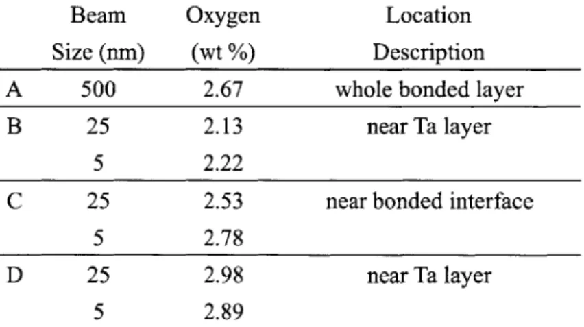
4-4 XTEM images of the Cu-Cu bonded layer: (a) low magnitude image, (b) no observable interface, (c) zigzag interface, (d) drastically changing fluctuation depth, (e) the smooth interface with a smaller fluctuation depth, and (f) continuous tw ins... 54 4-5 XTEM image for EDS tested areas... 57
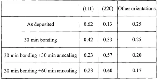
5-1 XEM images of the Cu-Cu bonded layer and the major diffraction pattern of single grains for selective area: (a) before bonding (b) after 30 min bonding (c) after 30 min bonding and annealing... 61
5-2 Average grain sizes as a function of different bonding conditions. Five wafers were investigated for each condition. Bar represents range of data... 62
5-3 Various of XEM images of the Cu-Cu bonded layer after 30 min bonding... 63
5-4 XRD patterns for different bonding conditions... 65 6-1 TEM morphologies of (a) "Grain" (bonded at 350C for 30 min followed by N2
annealing for 60 min), and (b) "Interface" (bonded at 350C for 30 min)... 71 6-2 Schematic diagrams of three catalogues for possible TEM observation results of
Cu bonded layer (a) No interface but grain structure (identified as "Grain"), (b) Interface structure (identified as "Interface"), and (c) Failure of TEM sample (identified as "TEM failed")... 72 7-1 Morphology and strength map for copper wafer bonding under different
bonding temperatures and conditions... 85
7-2 Results of bonding strength under different bonding conditions by pull test.
Some of bonded samples above 3000C did not break along the bonding
interface but along other thin film interfaces. Bars represent range of data, and offset from the average point for visual conveniences... 87 7-3 Schematic diagram of the shear test... 91
7-4 Results of bonding strength under different bonding conditions by shear test. Some of bonded samples above 300'C did not break along the bonding interface but along other thin film interfaces. Bars represent range of data, and offset from the average point for visual conveniences... 92
8-1 An example of wafer bow evolution during the heating process from room temperature to 400'C. The value of " A Wafer Bow" means the difference of
wafer bow relative to initial wafer bow... 97
8-2 The relation of wafer bow and bonding quality at different bonding temperatures. Average wafer bow means the average wafer bow of two wafers to be bonded ... 106
9-1 SEM image of 10 tm-wide Cu bonded interconnects... 110
9-2 TEM image of 5 pm-wide Cu bonded interconnect... 110
10-1 Schematic diagram of the contact resistance test structure... 113
10-2 Top view of (a) our contact resistance and (b) Kelvin test structure... 114
10-3 Schematic diagrams of (a) the conventional Kelvin structure with misalignment, and (b) the test structure used in this work... 114
10-4 The process flow of the test structure for contact resistance measurement... 116
10-5 Top view and dimensions of the test structure... 117
10-6 Average Cu-Cu bonded specific contact resistances as a function of interconnect size for different bonding conditions... 119
10-7 The corresponding specific contact resistance of bonded 5-pim-wide interconnects without pre-bonding HCl treatment when stressing current was ramped gradually from 1 mA to 100 mA at the rate of lmA/s. The interconnects were bonded at 400 C for 30 min followed by 400 0C N 2 anneal for 60 m in... 120
10-8 The electrical yield as a function of interconnect sizes for different bonding con dition s... 122
10-9 The corresponding specific contact resistance of some bonded interconnects
with pre-bonding HCL clean at the rate of ImA/s for wafers with (a) 5, (b) 7 and (c) 10 tm-width interconnects bonded at 400 C for 30 min followed by
400 C N2 anneal for 60 min... 123 10-10 AFM surface morphologies of Cu interconnects (a) without and (b) with HCl
clean before bonding. "A" area shows an abrupt peak and "B" area represents
a generally rough area... 125
11-1 The relation of bonding percentages and interconnect sizes under different
total bonding areas... 132
11-2 The relation of bonding percentages and total bonding areas under different
interconnect sizes... 134
11-3 Schematic diagrams of normal design for placement of electrical interconnects
only and a new design for placement of electrical interconnects and dummy
pads on the sam e w afer... 136 11-4 The relation of bonding percentages and different designs of interconnects and
dummy pads using different interconnect sizes... 138
12-1 Schematic diagram of fabrication flow for the bonded structure... 142 12-2 TEM image of a two-wafer-bonded structure after grind back, etch back and
C u/Ta deposition... 145
12-3 TEM image of a four-wafer-bonded structure after grind back, etch back and
C u/Ta deposition ... 148 12-4 Magnified TEM images of the (a) second and (b) third (middle and upper in
List of Tables
3-1 Results of razor test for bonded with different bonding conditions... 45
4-1 EDS examination for oxygen in different areas of the bonded copper layer... 56
5-1 The average fraction of grain orientations under different bonding conditions.... 65
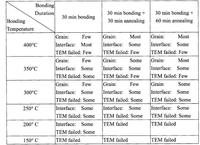
6-1 TEM results of the interfacial morphologies on Cu bonded wafers under different bonding conditions... 73 7-1 Number and percentage of failed pieces at different bonding conditions after
dicing process... . 81 7-2 Number and percentage of total failed pieces at different bonding conditions
after dicing process and tape test... 86 8-1 Average change of wafer bow at different temperature relative to the wafer bow
after Ta and Cu film deposition... 98 8-2 Relative dicing failure percentages of bonded wafers with different initial wafer
bows when these wafers were bonded at 200'C (One wafer: 262 pieces)... 100 8-3 Relative dicing failure percentages of bonded wafers with different initial wafer
bows when these wafers were bonded at 300'C (One wafer: 262 pieces)... 102 8-4 Relative dicing failure percentages of bonded wafers with different initial wafer
10-1 Comparison of contact resistance and specific contact resistance for Cu-Cu bonding at 400 C bonding for 30 min followed by 400 C N2 anneal for 60
min (this work), metal-metal and metal-Si interconnects [101, 102]... 119
10-2 Electrical yield of different interconnect sizes of test structures. Bonding condition was 30min bonding at 400'C followed by 30 or 60 min nitrogen anneal at 400'C. Samples of each condition were collected from three wafers.
Chapter 1
Introduction
1.1
Motivation
In order to extend integrated circuit (IC) performance beyond device and interconnect scaling limits, new integration approaches are being explored. Interconnect performance will become more dominant in the system performance of integrated circuits (ICs) as the
critical dimension in integrated circuits keeps shrinking [1]. For the purpose of meeting the projected system performance demands, innovative system architecture or new interconnect materials need to be developed. Although new interconnect materials and low-K materials offer improvements in system performance, their contributions are limited. A novel design of system concept, architecture, and fabrication technologies will be required in order to significantly improve and even solve problems such as signal delays [2] by keeping the wire-length short at a high clock speed [3-7]. Three-dimensional (3D) integration, in which multiple layers of devices are stacked with high density of interconnects between the layers, is an attractive candidate for a source of
solutions for these problems [8, 9].
1.2
Three-dimensional (3D) Integration
The concept of three-dimensional integration was first proposed in the 1980s [10-12]. Three-dimensional integration provides more functionalities within a smaller footprint, and may further reduce chip size [8]. This advantage is especially attractive for wireless and military applications. In addition, for integrated circuits, performance such as signal delay and clock skew can be effectively improved with a reduced total interconnect length in three-dimensional integration [13-16]. Thus, the wire length between microprocessor and memory can even be greatly reduced by using three-dimensional integration. Finally, flexibility in device technology and materials selection is also provided through the parallel processing of separate layers or wafers, which are finally stacked together using three-dimensional integration fabrication. Therefore, it becomes possible to stack analog and digital design on different layers together, or optoelectronic and electronic devices on different material substrates together.
Three-dimensional integration can usually be divided into two categories: 3D packaging and 3D IC. 3D packaging is the stack of dies or multi-chip modules (MCM)
[17, 18]. In fact, 3D packaging is the idea for decreasing the wire length of chip-to-chip.
Some concepts of 3D packaging propose that the total interconnect density can be higher
by conducting vertical through-hole vias [19, 20]. Today packaging companies are
pushing this concept from R&D to manufacturing. 3D IC, which offers layer-to-layer (level-to-level) interconnect connections, provides even shorter wire-length than 3D packaging. This thesis focuses on the wafer level of three-dimensional integration,
especially possible applications for 3D IC.
For wafer level 3D integration, sequential and parallel approaches have been proposed to fabricate devices [21]. The purpose of these approaches is to build a vertical silicon layer stacking with strong structure and reliable performance. Sequential approaches are that layers with devices are fabricated sequentially [22-23]. The process starts with the first device layer on the substrate, then second layer is formed on the top of first layer and devices are fabricated. This process can be repeated for the sequent layers. Several sequential approaches have been proposed based on recrystallization [9, 24], metal-induced lateral crystallization [25-30], germaniem seeded laterally crystallizated technologies [31-32], and epitaxy growth [33] to form another Si layer on the top of device layer. There are two major drawbacks in sequential approaches. One is the performance of upper device layer may be reduced because of the bad quality of polycrystalline silicon for the upper layer. The other one is the issue of thermal cycling during fabrication may degrade the performance of devices as well. Although the first drawback recently can be improved by seeded laterally crystallizated technologies to form a single grain to avoid the defect problem [31-32], thermal cycling, which may introduce large stresses in the structure, is still a major concern while applying this technology for 3D applications.
While sequential approaches still have concerns to overcome, parallel approaches offer another choice to solve this problem. Parallel approaches to achieve three-dimensional integration are usually based on bonding of separate wafers together combining a process of substrate removal or layer transfer [34]. Therefore, the upper device layers can be fabricated separately. Afterwards, the upper layers can be transferred on the top of bottom layer by bonding. The choice of bonding materials depends on
different fabrication approach. Silicon-to-silicon [35-36], metal-to-metal [37-40], and polymer-to-polymer [41-47] are potential candidates. One big challenge of the approaches with wafer bonding is to achieve a strong bond strength and quality and at the same time the bonding conditions should be compatible to the underlying device layers.
While three-dimensional integration has several significant potential advantages over other monolithic techniques, challenges, such as alignment, process reliability, thermal stress and heat transfer exist [48-50]. Among these challenges, process reliability is one of the most significant. In addition, in order to implement a variety of applications, three-dimensional integration should stack and interconnect more than two layers. Therefore, a reliable process is key to achieve a high number of stacking layer structure in three-dimensional integration.
1.3
MIT Three-Dimensional Integration
The MIT three-dimensional integration is based on direct Cu-Cu wafer bonding at low temperature [40]. Device wafers, with Cu interconnects for electrical connectivity and Cu pads for structural support, are sequentially bonded each other in a face-to-back approach using Cu-to-Cu low temperature thermal compression.
The process flow for fabricating monolithic 3-D ICs is illustrated in Figures 1-1(a) and (b). The significant steps shown in Fig. 1-1(a) are described as followed:
1. Fabrication of device layers on a SOI Si wafer.
2. In order to stack the device layer on the top of another device layer, the substrate of
SOI wafer has to be thinned by grinding and etching process. During the grinding
wafer under three requirements: (a) the adhesion of handle wafer and SOI is strong enough to withstand the stress during grinding, (b) the adhesion is inert to the solution using in etching SOI substrate process, and (c) the adhesion can be removed by a solution easily, but the solution does attack other materials in the structure.
The handle wafer is prepared by coating silicon nitride on both sides of Si wafer to protect the structure from future etching process. Then Al and Cu films are sequentially deposited on both the handle wafer and SOI wafer. After bonding handle wafer and SOI wafer by Cu-Cu bonding, the handle wafer is attached.
3. The thin back process to remove the Si substrate of SOI wafer is a combination of
mechanical grindback and chemical etching, which will stop on the buried oxide of
SOI. The chemical etching solution can be either KOH or TMAH [51, 52].
4. Once the completion of the removal of SOI substrate, inter-vias are created by etching the oxide, SOI and ILD.
5. The PECVD oxide sidewall passivation and via filling using damascence are
performed.
6. Cu interconnects are deposited on the top of vias for electrical connectivity. In
additions, dummy Cu pads can be also patterned to increase the bonding strength of the whole structure. To this step, the device layer attached to the handle wafer is treated as upper wafer for the next bonding process.
7. Fabrication of device layers, including the patterning of Cu interconnects and pads,
on a bulk Si wafer. This bulk Si wafer with device layer is treat the bottom wafer. Then the upper wafer and bottom wafer is aligned and bonded at the desired bonding condition. The detailed alignment and bonding process will be described in Chapter 2.
bonded wafer in the HCl solution, Al film will be dissolved in HCl but at the same time all other materials are inert to the solution [53]. Therefore, the handle wafer will separate from the bottom wafer. The device layer attached to the handle wafer will be remained bonding to the device layer of the bottom wafer.
1. Cu patterning on SOl
device wafer
- m
4. Etch vias
2. Bond to handle wafer
5. Via filling
uNr Wn..a
3. Thin back SOl wafer;
stop on buried oxide
t
C
tt
6. Cu patterning MONIE. 7. Bond to another device waferI
I Iill
I I I I8. Release handle wafer
9. Repeat process #1
~
#6 for 3rd active layer
3rd active _ ___ 2nd active layer - "n 1st active layer Ine MN layer10. Bond 3rd active layer to
1st and 2nd active layers
munmmmumm muwm.e.
uuMen monm UUE e u mlU
3rd active layer 2nd active layer 1st active layer
11. Release handle wafer
12. Repeat process #1
~
#6 for 4th active layer
mosMEu 4th active __ __ _ layer -- m-m- . a I 3rd active SOO-layer u . 2nd active mmmlmm m layer
1st
active layer13. Bond 4th active layer to
1st, 2nd and 3rd active layers
!Em.-
I.
:
.
.
W.I
uma a 10IMIS-I-ENA Sm o 4th active layer 3rd active layer 2nd active layer 1st active layer
14. Release handle wafer
Two device layers are successfully bonded after step 8. If more than two device layers are required, this two-bonded-device-layer wafer can be treated as the bottom wafer and third-device-layer wafer can be prepared by repeating steps 1 to 6. Figure
1-1(b) illustrates the subsequent steps for a four-active-layer stacking structure. This
structure can be treated as three-dimensional integrated circuits.
1.4 Wafer Bonding
Wafer bonding has been used in silicon on insulator (SOI) and microelectromechanical systems (MEMS) applications [34, 39]. In addition, wafer bonding is a key technology for development of three-dimensional integration [39, 40]. The ability of wafer bonding to create a good bonding quality across the wafer enables the possibility of heterogeneous integration of devices. There are three types of wafer bonding: direct wafer bonding (also called fusion bonding), anodic bonding, and thermocompression bonding (also called intermediate-layer bonding) [34].
Direct wafer bonding means the process of bonding wafers without an intermediate adhesion layer. The wafer surfaces should be kept clean and flat to get the best bonding quality. The process requires an initial contact of two wafers. In some cases, heat treatments may increase the bonding strength. Surface treatment, such as plasma etching, and solution cleaning, is conducted before the bonding process to promote the surface attraction.
Anodic bonding involves one silicon wafer and one glass wafer that has alkali metals. This process is completed by the application of an electric field between the two wafers at temperatures ranging up to 500 'C. Attention is paid to ensure the same range
of thermal expansion coefficients of glass and silicon.
Thermal-compression bonding using an intermediate layer such as metal films has been used in packaging level applications [46, 47]. Solder bonding for wiring bonding during the packaging process is the typical example [40]. In addition, eutectic bonding that utilizes the eutectic properties to create a reliable bond during bonding is proposed in Su and Au thin film applications. For wafer level bonding, thermalcompression bonding enables the connections of different wafers via metal line bonding with short distances.
Wafer bonding has attracted a lot of attention for future device applications, especially the potential benefits of high performance, compact size, and low cost. In order to achieve these benefits, improvements of cleanliness, alignment, vacuum and yield of the bonding facility is the first topic. Potential material issues, such as stress and defects, need to be solved as well. These challenges are significant before wafer-bonding technology becomes a production technique.
1.5
Advantages of using Cu as the bonding material
Because integrated circuit interconnect dimensions keep shrinking, copper is a promising candidate of interconnect metallization materials for advanced electronic applications to replace aluminum. Since copper has higher electrical conductivity than aluminum, and the thermal conductivity ratio of copper and aluminum is approximately 2:1, copper can improve the electrical performance, reduced Joule heating, and better heat transfer. The electromigration problem in copper should be less than in aluminum since copper has the higher melting point [54]. Therefore, copper is rapidly developing into the material used in mainstream interconnect technologies.
As mentioned in previous sections, there are several bonding materials for three-dimensional integration. Each bonding material has a different specific bonding approach. For some approaches using silicon or polymer as bonding materials, blank oxide or polymer is deposited on the top of the active layer of each wafer without any patterns. Then after bonding the wafers together, a subsequent etching process to define through-hole vias, which penetrate the whole wafer, is performed. Finally vias are filled with copper. Since the aspect ratio of via is too big, it is difficult to perfectly fill the vias and control the cleanness condition in the bottom of the vias. These two concerns bring issues, such as open circuits and high contact resistance, respectively.
Copper wafer bonding in three-dimensional integration patterns the copper interconnects individually on separate wafers, and then bonds them together. The thickness of Cu layer used in this thesis is 300 nm. Thus the issue of filling the vias with
copper due to high aspect ratio in this approach does not exist.
Moreover, compared to oxides or polymers with poor thermal conductivities, copper has an excellent value and thus the copper bonded layer can act as a heat conduit. Besides,
the bonded layer can be treated as another metal layer while other approaches do not have this advantage. Finally, copper bonding offers not only the electrical connectivity but also mechanical support. In addition to copper interconnects, an idea to place copper dummy pads in the used areas to increase the mechanical strength is proposed and will be further
discussed in Chapter 11.
Based on the above discussions, copper as the bonding material in three-dimensional integration has advantages in different areas and is a promising candidate to fulfill three-dimension integration applications.
1.6
Research Goal and Contribution of Thesis Work
Three-dimensional integration promises to improve circuit performance while device scaling faces fundamental limitations. Since the application of three-dimensional integration has to be based on current semiconductor process technologies, while using copper wafer bonding, compatible process parameters such as the highest process temperature and pressure need to be considered to avoid the destruction of device structure or the degradation of circuit performance. Selection of solutions in subsequent etching processes to avoid the reaction with existing device materials is significant as well.
Since the bonding material is copper, the source of structure strength in three-dimensional integration is based on the result of copper bonding. Copper bonded interconnects are also the media for electrical current to pass through. The electrical performances such as contact resistance may be influenced if copper bonding is not
satisfactory.
Moreover, three-dimensional integration is used for the device applications. The expense of the bonding process should be kept as low as possible. A long bonding process, which increases the total process time of a device, is not an acceptable solution for industries.
The research goal, based on the above discussions, is to develop a reliable copper wafer bonding in three-dimensional integration. Copper bonding should have strong bond strength and excellent electrical performance. In the bonding process, temperature should
be as low as possible and duration should be as short as possible. Bonding temperature,
circuit performance.
This thesis work involves fundamental studies of copper wafer bonding and bonding performance of bonded interconnects. In addition, process development of silicon layer stacking based on copper wafer boAding is applied to demonstrate a strong four-layer-stack structure. This process development can be reliably applied in three-dimensional integration applications. Based on the results of research works including bonding quality and bonding parameters, bonding conditions with different considerations are suggested for applications.
1.7
Thesis Organization
The outline of this thesis work is as follows:
Chapter 2 of this thesis describes the detailed bonding process and other experiments that were frequently used. Other experiments for bonding interface observation, material property measurements, and bonding quality investigations are described as well.
Chapter 3 reports the initial results of copper wafer bonding using razor test. The results offer information for initial bonding condition selection in this thesis.
In Chapters 4, 5, and 6, the bonding interfacial morphologies with different bonding conditions are studied. Detailed microstructures, material properties, and evolution of bonded layer are also investigated.
Chapter 7 studies the bonding quality and bonding strength using different techniques. Based on the results in previous chapters, a map summarizing the bonding quality is established.
In Chapter 8, effects of wafer bow on bonding quality are investigated. In the end of the chapter, criteria are provided for future wafer selections.
In Chapters 9, 10, 11, and 12, the research field of copper wafer bonding is moved from blank copper wafer bonding to bonded copper interconnects. In chapter 9, microstructures of copper bonded interconnects are observed.
Chapter 10 and 11 report the contact resistance measurement and bonding quality of copper bonded interconnects, respectively. A novel design of test structure for contact resistance measurement is described. Sizes of interconnect, total bonding area, and the uses of dummy pads are factors to affect the bonding quality.
Chapter 12 describes the process development of silicon layer stacking using copper wafer bonding, grind back, and etch back. Morphology investigation and possible issues are discussed as well.
Chapter 13 summarizes the results of the study including bonding quality and bonding parameters. In the end, suggestions of bonding conditions are made for applications.
Chapter 2
Bonding
Process
and
Other
Description of Experiments
This chapter describes the detailed bonding process and other experiments that this thesis frequently uses. The description starts with the initial wafer selection and surface cleaning preparation. Procedures of metal deposition, metal surface cleaning prior to bonding, detailed bonding and anneal procedures are described as well. The last section describes different techniques to investigate bonding morphology, materials properties, bonding strength, and electrical performance measurement. Specific experimental procedures for different project will be described separately in each chapter.
2.1
Initial Wafer Preparations
Single crystal, n-type (2-3 Q-cm) and p-type (8-12 Q-cm), 4-inch (001)-oriented silicon wafers were used in the present study. Before the next process, surfaces of Si wafers were cleaned to remove native oxides and particles. The cleaning process was carried out with a wet bench. The wafers were first cleaned in a solution A (H2SO4: H202= 3 : 1) for 10
min at 120'C to grow a thin layer of SiO2 which was etched away by immersing the
wafers in a dilute HF solution (HF : H20 = 1: 50) followed by a de-ionized water rinse.
Next the wafers were cleaned by a solution B (NH40H : H202: H20 = 1: 1 : 5) for 10
min. at 75'C and dipped in a dilute HF solution (HF : H20 = 1:50) followed by a
de-ionized water rinse. Then the wafers were cleaned by a solution C (HC1 : H202: H20
= 0.25 : 1 : 5) for 10 min at 750C and dipped in a dilute HF solution (HF : H20 = 1: 50)
followed by a de-ionized water rinse. Finally, the wafers were dried in a spinner.
2.2
Thin Metal Films Deposition
The metal films were evaporated with an AIRCO Temescal STIH-270-1 electron gun evaporation system with maximum power about 7 kW. The electron beam, accelerated by a voltage of 8.2 kV, was directed onto the hearth by means of a magnetic field that bent the beam 2700 downward. During the evaporation, the top layer of the source in the crucible was melted and evaporated onto substrates by the electron beam. The source crucible was water-cooled to prevent the contamination of the source by crucible materials or other impurities. The thickness and rate of deposition could be read directly from the display of a microprocessor unit connected with a quartz sensor produced by
INFICON. The accuracy of the measurement was about 0.1 nm.
The vacuum system used is an AIRCO Temescal model BJT- 1800 system, which is equipped with a 6-inches diffusion pump and a liquid nitrogen cold trap. Optimum
vacuum of 1x10~7 Torr was attainable. During deposition, the vacuum was maintained to be better than 1x10⁻⁶ Torr. The deposition rate was about 0.3 nm/sec.
beam deposition. The Ta layer acts as a Cu diffusion barrier up to 550'C [55].
2.3
Copper Surface Cleaning
In previous studies, surface preparation for metal-to-metal bonding is an important factor to achieve a good bond [56]. In this research, metal surfaces of some wafers were cleaned prior to bonding. Wafers needing removal of surface oxides after Cu deposition were dipped in 1:1 (by volume) H20:HCl for 30 s followed by a DI water rinse and spin dry.
Any native oxide on the Cu surface should be removed through this process. Reactions for HCl and surface oxides are shown as follows [57]:
Cu2O(s) + 8C- + 2H+(aq)
+
2CuC142 -(aq)+H20(1)+2e-CuO(s) + 4C- + 2H+(aq) 4 CuCl42-(aq)+H20(l)In Section 2.1, the cleaning of silicon surfaces ensures high quality and clean surfaces without particles prior to the deposition process, while the cleaning of copper
surfaces is to create clean metal surfaces before bonding process.
2.4
Optical Wafer-Wafer Alignment
The bonding targets belonging to separate wafers need to be aligned before bonding in order to acquire the accuracy of circuit placement. This alignment is especially important when the dimension of bonding media is small. Any misalignments will cause the decrease of bonding strength and failure of circuits.
started by clamping two wafers together face-to-face, with the wafers separated by three 30- tm metal flaps on the bonding chunk. Afterwards, the chuck with the wafers is ready to bond. Figure 2-1 shows the schematic diagram of alignment procedures [58].
2.5
Bonding Process
The bonding process was carried out in the Electronic Vision AB 1 -PV bonder. The chuck with the wafers was placed in the EV bonder. The N2 was purged before the chamber was
evacuated to 10-3 torr. A 300-mbar force was then applied at the center of the top wafer while the flaps were pulled. When the wafers were in full contact, a 1000-mbar force was applied while both wafers were being heated at a rate of 40'C/min. Once the temperature reached the desired bonding temperature, a 4000-mbar force was applied for the desired bonding duration. Afterward, it required 2 hours to cool the wafers to room temperature.
2.6 Anneal
Bonded wafers needing further annealing were placed in a diffusion furnace in N2
Physical
Alignment marks
S-- 'Circuit layer
W w Microscope 1 objectives
1. Insert top wafer,
circuit-side down
Alianer CRT Displav
Top SI
il w
2. Insert bottom wafer,
circuit-side up. Wafers are
separated by three - 30 pm
metal flap
oto Si
+ +
3. Align bottom wafer
to computer marks --- U- __ *
I
I
mmum4mmuumi.wulmi.wm.m U I I * U * U * 3 * I * I * I * I Computer Alignment Marks1. Align computer generated
marks to physical marks
* I * I * I * 3 * I * I * B * U 3 I * I * S * I
2. Bottom wafer mis-aligned 3. Both wafers aligned
Figure 2-1 The schematic diagram of alignment procedures [58]
37
2.7
Bonding Strength Examinations
2.7.1 Dicing Test
The dicing process is the tool to examine the bonding strength of Cu bonded wafers. Bonded wafers were cut into 5mm x 5mm square dies at a speed of 0.69 mm/sec by a
DAD-2H/6T Automatic Dicing Saw. If the bonded piece separates after dicing, the
bonding strength is qualitatively decided.
2.7.2 Tape Test
Surviving bonded pieces after the dicing test underwent the tape test. The 3M Scotch
3710 Adhesive Tape was stuck on the bonded pieces. Then force by hands was applied to
rip the tape from the piece. If the bonding strength is larger than the adhesion between the adhesive tape and piece, the tape will separate from the piece. If the bonding strength is smaller than the adhesion between the adhesive tape and piece, the piece will break from the bonding interface and the tape will remain stuck to one of the separating pieces.
2.7.3 Pull Test
Surviving bonded pieces after dicing test underwent the pull test by a Guad Group Romulus III Pull Machine. One side of the bonded piece was loaded on the substrate of the machine, while the other side was glued to a pin with Epoxy. During the pull test, the machine pulled the pin until the sample broke. The force at the failure of the sample was recorded.
2.7.4 Shear Test
Surviving bonded pieces after dicing test underwent the shear test by a Dage Series 4000 Shear Machine. The bonded piece was first loaded on the substrate of the machine. Then a board perpendicular to the substrate was raised to a "shear height" of 600 pim. Shear height means the distance between the bottom of the bonded piece to the bottom of the board. During shear test, the board pushed the upper part of the bonded piece until the
sample broke. The force at the failure of the sample was recorded.
2.8
Scanning Electron Microscope Observation
The morphologies of copper bonded wafers, which present grain structures, defects, and bonding interface, were observed with a JEOL 6320FV Field-Emission High-Resolution Scanning Electron Microscope (SEM).
2.9
Transmission Electron Microscope Observation
2.9.1 Cross-Sectional Specimen Preparation
XTEM samples were prepared by a modified Sheng's method [59]. The step-by-step procedures are described as follows:
1. The samples were cut into 3 mm x 2 mm rectangular pieces.
2. The pieces were lapped from the back surface to a thickness less than 60 ptm.
holder was used to squeeze out the epoxy so that only a thin layer of epoxy, about 0.1 mm in thickness, was left between the samples. Two protective silicon wafers were also cut into 3 mm x 2 mm rectangular pieces and bonded together with the samples. 4. Stack was then mounted on a blank silicon piece.
5. Sample assembly was polished sideways sequentially by 1200-grit abrasive paper, 15 tm and 3 pm diamond pastes.
6. The polished surface of the stack was then mounted with a thin layer of
CRYSTAL BOND on a glass piece.
7. The new specimen assembly was then lapped from silicon side to less than 10 pm thick using, in succession, 400-, 800-, 1200-grit abrasive papers and 3 pm diamond paste.
8. A copper mesh, 3 mm in diameter, was bonded by epoxy to the sample stack.
9. The silicon material and wax outside the boundary of copper mesh were removed with tweezers.
10. The CRYSTAL BOND was dissolved with ACE. Sample stack with copper ring was then detached from the glass piece. Finally, the exposed side of the sample was bonded by epoxy to another copper mesh.
11. Both surfaces of the sample stack were milled by argon ions until a hole developed near the center of the sample. The argon ion energy, milling angle and ion current were 5-6 keV, 12-15' and 50-200 p.A, respectively. It should be noted that during the ion milling process, the samples were kept below 120 'C to avoid grain growth [60].
2.9.2 Transmission Electron Microscope Observations
A JEOL-200CX scanning transmission electron microscope (STEM) and JEOL-2010
transmission electron microscope operating at 200 kV were used for conventional TEM examination. Most of the micrographs were taken under two beam diffraction conditions with deviation parameter Sg slightly positive. Most of the XTEM micrographs were taken along [110] zone axis of the Si substrate.
2.10
Energy Dispersion Spectrometer (EDS) Analysis
Energy Dispersion Spectrometer (EDS) Analysis, a Link ISIS energy dispersive analysis of the X-ray instrument attached to the JEOL-2010 TEM, was used to determine the compositional distribution of oxidation in local areas of samples in the Cu bonded layers [59]. Various beam sizes and a process time of 100 sec were chosen for EDS analysis for the samples.
2.11
Atomic Force Microscope (AFM) Observation
The surface morphologies and surface roughness of Cu films with or without any surface treatment before bonding were examined with an Autoprobe CP atomic force microscope (AFM).
2.12
X-ray Diffraction (XRD) Analysis
The crystallography, which is also grain orientation, of the Cu bonded layer after different bonding condition was analyzed by X-ray diffraction (XRD) [Rigagu D/Max] with Cu Kc radiation.
2.13
Wafer Bow Measurement
Wafer bow is obtained from the measurement of the overall magnitude of wafer curvature, and usually means the height deviation between the center of the wafer and the edge of the wafer. Wafer bows were measured using a KLA-Tencor thin film stress measurement. This equipment can be operated at different temperature.
2.14 Electrical Properties Measurement
A four-point probe station was used to stress current and measure the voltage drop of the
testing samples. An HP 4156 Semiconductor Parameters Analyzer was used to ramp a current between 1 mA and 100 mA on the test structures.
Chapter 3
Initial Results of Copper Wafer
Bonding
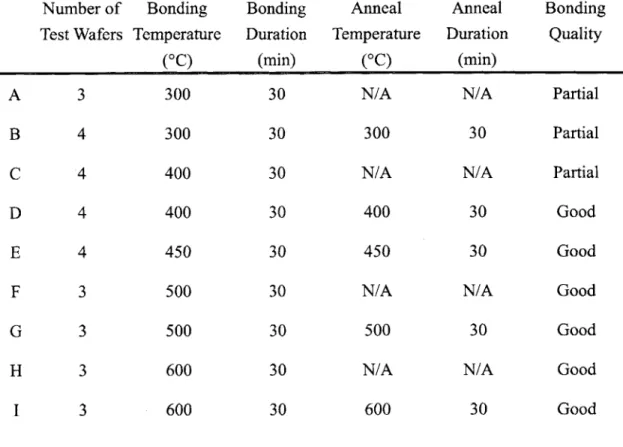
In order to successfully fabricate three-dimensional integration applications using copper wafer bonding, the quality of copper bonded wafers should be strong and able to support the structure during subsequent processes. In addition, the bonding process should not affect any existing devices in the wafers. Therefore, developing a reliable copper wafer bonding is the key role in three-dimensional integration. To achieve a reliable copper wafer bonding, the bonding quality and other properties such as material and electrical performances under different bonding parameters must be investigated. The razor test is used to examine the copper wafer bonding quality and offers the initial results for the rest of this thesis.
3.1
Razor Test
Before studying the bonding quality and bonded layer properties, initial results of copper wafer bonding were examined. Razor test is a good candidate for qualitative study. In the razor test, the strong bonding means the razor cannot penetrate the bonding interface [61]. Razor test for copper wafer bonding was developed by A. Fan in MIT to examine the bonding qualitatively [62]. The bond strengths can be categorized as follows: A good bond means the wafers are inseparable and the razor does not penetrate the bonding interface. In general, the wafer fractures are small fragments and located in the edge area. This good quality is comparable with that of silicon-silicon wafers bonded at high bonding temperature. Partial bond means the bonded wafers separate from the bonding interface completely or in large area when a large force is applied to the razor. Poor bond means the bonded wafers could separate from the bonding interface easily with a small force applied to the razor or the wafers did not bond at all [62].
3.2
Initial Test Results
According to the results reported in ref. [62], detailed bonding parameters were carefully selected for razor test. Based on the operating parameters of Electronic Vision AB1-PV bonder, the bonding temperature was from 300'C to 600'C; the bonding pressure was at 4000 mbar; and the bonding duration was 30 min. Optional nitrogen
anneal after bonding was performed at the temperature of bonding for 30 min.
Table 3-1 shows results of razor test for bonded wafers with different bonding conditions. The experiment was based on the previous results of razor test on copper
bonded wafers [62]. Three or four wafers of each bonding condition were investigated.
Table 3-1 Results of razor test for bonded with different bonding conditions.
Number of Bonding Bonding Anneal Anneal Bonding
Test Wafers Temperature Duration Temperature Duration Quality
(OC) (min) (*C) (min)
A 3 300 30 N/A N/A Partial
B 4 300 30 300 30 Partial
C 4 400 30 N/A N/A Partial
D 4 400 30 400 30 Good
E 4 450 30 450 30 Good
F 3 500 30 N/A N/A Good
G 3 500 30 500 30 Good
H 3 600 30 N/A N/A Good
I 3 600 30 600 30 Good
Results of razor test show that the bonding quality increases with the increase of bonding temperature, the increase of bonding duration, and the use of nitrogen anneal after bonding. Reliable good bonding quality of copper bonded wafers can be found in the bonded wafers that were bonded at 400'C for 30 min followed by nitrogen anneal at 400'C for 30 min. The bonding quality remained as the bonding temperature was higher than 400'C. Because of the preference for low process temperature in industry, the bonding condition: "400'C bonding for 30 min at 4000 mbar plus 4000C nitrogen anneal for 30 min", with the good bonding quality at the lowest temperature in Table 3-1, was chosen for the fundamental studies in this thesis such as interfacial morphology
Chapter 4
Microstructures of Copper Bonded
Layer
In previous section, the preliminary result of the quality for bonded wafers has been testes by the razor test. Although it shows that copper wafers can be bonded reliably as low as 400'C at 4000 mbar for 30 min and followed by a 30 min N2 anneal at 400'C for 30 min with the test, detailed interfacial microstructure observation of the bonded layer to
support this result. If the interfacial morphology shows the two copper layers are bonded, the evidence of good quality bonding is more solid. In this chapter, the microstructure morphologies and oxide distribution of copper bonded wafers at this bonding condition were examined by means of transmission electron microscopy (TEM) and energy dispersion spectrometer (EDS).
4.1
Sample Preparation and Experimental Procedures
(100) Si wafers were deposited 300 nm Cu and 50 nm Ta films were deposited with an
electron beam deposition. After dipping in HCl for 30 sec, the wafers were bonded at 400'C with a 4000-mbar force for 30 min followed by annealed in diffusion furnace in
N2 ambient for 30 min at 400'C. Detailed experiments of theses processes are described
in Chapter 2. The morphologies of the Cu-Cu bonded wafer interface were examined with a JEOL-200CX scanning transmission electron microscope (STEM) and JEOL-2010 transmission electron microscope. Energy Dispersion Spectrometer (EDS) Analysis, a Link ISIS energy dispersive analysis of the X-ray instrument attached to the JEOL-2010 TEM, was used to determine the compositional distribution of oxidation in local areas of samples in the Cu bonded layers. Various beam sizes and a process time of 100 sec were chosen for EDS analysis for the samples.
4.2 Interfacial Morphologies
4.2.1 TEM Observation
Figures 4-1 and 4-2 show the cross sectional transmission electron (TEM) images of the Cu-Cu bonded layer. This wafer was bonded at 400'C and 4000 mbar for 30 min. and then annealed at 400'C for 30 min in N2 ambient atmosphere. In Figure 4-1, the TEM
sample was taken from the center of the wafer, which shows a well-bonded layer. Random interfaces, grains, and defects are observed but no voids or vacancies are found. In Figure 4-2, however, the TEM sample was taken from near the edge of the wafer. A
mixture of good bond and unbonded areas is observed in this Cu-Cu region. The actual sizes of the voids and unbonded voids were smaller since enlargement of vacancy sites were probably caused by ion-milling of the TEM sample during sample thinning. It should be noted that this morphology is only observed once in ten TEM sample observations at this bonding condition.
The microstructures of the well-bonded layer were examined by TEM, as shown in Figures 4-3(a) and (b). The condition of the samples is the same as that in Figure 4-1. Different kinds of defects were observed: stacking faults, twins and dislocations were formed in the bonded layer with different directions. Two groups of defects with different directions are observed in Figure 4-3(b). One group is parallel to the metal layer formed along the Cu-Cu interface. The other group is continuous twins with 75 degrees respect to
Si substrate that penetrates the bonded layer.
Si
300 am
Figures 4-1 XTEM image of the Cu-Cu bonded layer. This wafer was bonded at 400'C and 4000 mbar for 30 min. and then annealed at 400*C for 30 min in N2 ambient
atmosphere. Image was taken from the center of the wafer.
Si
Ta
Ta
Si
3 pim
Figures 4-2 XTEM image of the Cu-Cu bonded layer. This wafer was bonded at 400*C and 4000 mbar for 30 min. and then annealed at 400*C for 30 min in N2 ambient
atmosphere. Image was taken from near the edge of the wafer.
4.2.2 Discussion
Comparing Figures 4-1 and 4-2, a good bond area with no vacancies could be obtained at the center of the bonded wafer. A partial bond area, where vacancies and good bond areas mix, occurs near the wafer edge. The different results come from the pressure profile distribution across the wafer, which produces uneven stress points during bonding. In our bonding apparatus, the full load pressure of 4000 mbar was applied to a metal plate by a piston located at the center of the wafers. The piston then creates a pressure wave emanating from the wafer center. The metal plate transfers the pressure profile to the wafers, and wafer- to-wafer contact occurs. It is reasonable to assume that the pressure applied on the edge of the wafer was less than the 4000 mbar applied at the center. Under the lower pressure, this area does not receive enough pressure to bond. Therefore, the Cu-Cu area of the edge of the wafer only could form a partial bond. Razor test results of
bonded wafers with bonding pressures less than 4000 mbar (1000, 2000, and 3000 mbar) provide the support of this assumption. Three pairs of bonded wafers were tested for each bonding pressure. From these razor test results, bonding qualities in bonded wafers with bonding pressures less than 4000 mbar were weaker than that with the bonding pressure
of 4000 mbar.
Si
500 nm
(a)
(b)