Adapting an LCD for Weight Generation in an
Electro-optic Neural Processor
by
Andrew Charles Lamson
B.S., EE, Massachusetts Institute of Technology (2011)
Submitted to the Department of Electrical Engineering and Computer
Science
in partial fulfillment of the requirements for the degree of
Master of Engineering in Electrical Engineering and Computer Science
at the
MASSACHUSETTS INSTITUTE OF TECHNOLOGY
June 2013
@)
Msachstts
Institute of Technology
2013.
All righits reserved.
A u th or ... %...
. . ..
....
...
Department of Electr
ngineering and Computer Science
May 28, 2013
Certified by ...
.--.-.-...-
. ...
...
Cardinal Warde
Professor of Electrical Engineering
Thesis Supervisor
Accepted by ...
...
4 ...Prof. Dennis M. Freeman
Chairman, Masters of Engineering Thesis Committee
Adapting an LCD for Weight Generation in an Electro-optic
Neural Processor
by
Andrew Charles Lamson
Submitted to the Department of Electrical Engineering and Computer Science on May 28, 2013, in partial fulfillment of the
requirements for the degree of
Master of Engineering in Electrical Engineering and Computer Science
Abstract
This thesis discusses adapting and testing an LCD as a weight image display for use in the Hybrid Electro-optical Neural Network (HENN). The HENN project is a proof of concept prototype hybrid neural network that will be used to gather information for a more advanced project in the future. After thoroughly explaining the HENN, this thesis characterizes the LCD selected for adaption. Within the characterization is a grouping of experiments that explore different aspects of the LCD screen. Then a few experiments are conducted to evaluate the interactions of the LCD and fiber optic interconnection plate. After this, the method used to generate the weighting image is explained thoroughly. The experimental evidence is gathered to show how the LCD can be used as a weighting system. Then based on the evidence gathered several recommendations are suggested to redesign the fiber plate and further improve the HENN system.
Thesis Supervisor: Cardinal Warde Title: Professor of Electrical Engineering
Acknowledgments
I would like to thank my thesis advisor Cardinal Warde for his encouragement and
guidance through all of my work. I would also like to thank Bill Herrington for his invaluable help and insight, and being there for every little problem and all the questions. I would like to thank my girlfriend Seoyeon Yang for her inspiration to pull through this busy time and to always aim for the better future. I would like to thank my sister for her consistent encouragement and familial concern, especially during our last semester in Boston. Finally, I would like to thank my parents for all their love and support through the years, I could not have done it without you.
Contents
1 Introduction
1.1 Background on Neural Networks . . . . 1.2 Project Background . . . . 2 The HENN System Architecture
2.1 Defining the HENN System . . . . 2.2 Fiber Optic Interconnection Plate . . . . .
2.9 LTCDTh a Sati1 CA TLight A-btor . .
2.4 Bistable Optical Device . . . .
2.5 Training Algorithm and Weighting System
3 Characterizing the LCD
3.1 LCD Specifications . . . . 3.2 LCD Pixel Analysis . . . . 3.3 LCD Spectrographic Analysis . . . .
3.4 Absolute Intensity and Pixel RGB Values .
4 Interfacing the Fiber Plate and LCD
4.1 Position-based Variation of Fiber Input Light Intensity . . . . 4.2 Single Fiber Loss . . . . 4.3 Effects of Crosstalk in the Fiber Plate . . . .
5 Creating the Weighting Image for Testing
5.1 Developing the Weighting Image Program . . . .
17 18 21 23 . . . . 23 . . . . 27 30 . . . . 31 . . . . 33 35 . . . . 35 . . . . 37 . . . . 39 . . . . 42 45 45 50 54 61 62
6 Conclusions
6.1 Recommendations for Optimization
6.2 Redesigning the Fiber Plate...
6.3 BOD-based Light Tests . . . . 6.4 Future Work . . . .
A MATLAB Code Appendix
A.1 Absolute Intensity versus RGB . . . A.2 Positional Intensity Variation . .
A.3 Weight Image Creation . . . . A.4 Weight Image Sizing . . . .
A.5 Weight Image Color . . . . A.6 Weight Image Saving . . . . A.7 Weight Image Main Method...
71 . . . . 72 . . . . 73 . . . . 81 . . . . 82 85 . . . . 85 . . . . 86 . . . . 90 . . . . 93 . . . . 94 . . . . 95 . . . . 95
List of Figures
1-1 Basic neuron model with four inputs. Image taken from [1]. . . . . . 19
1-2 Three layer neural network with three inputs, one hidden layer, and three outputs. Image taken from [1]. . . . . 20
2-1 This three layer neural network outlines the different partitions of the neural network for each type of layer. The partitions serve as a basis
for which HENN subsystems are used for each layer. . . . . 24
2-2 iagram UI the heoretical four layer "ENN. hi black
arr1ws-sent propagating light and the layers without light communicate elec-trically . . . . . 25
2-3 Left: Scaled 17 x 17 node array fiber plate first layer. Right: Zoomed in 2 x 2 node array to illustrate sizing. . . . . 28
2-4 Left: Scaled 17 x 17 node array fiber plate second layer. Right: Zoomed in 2 x 2 node array to illustrate sizing and ideal positioning of fibers. 29
2-5 Left: One node on the input side. Right: Nine nodes on the output side. Diagram for the Nearest Neighbor connection model employed in the HENN fiber plate architecture. The left grouping is a single node in the first/input layer of the fiber plate and the right grouping is the nine nearest nodes in layer 2 to the single node in layer one. Each smaller circle represents a single fiber and circles with the same number are the beginning and end of the same fiber. . . . . 30
3-1 Separated LCD panel from the Aluratek ADPF08SF digital picture fram e. . . . . 37
3-2 Two microscope pictures of the LCD pixels from the Aluratek ADPF08SF. The left is when all pixels are on and white, while the right is a black and white checkerboard pattern. . . . . 38
3-3 On the left: the Red Green Blue composition and sizing of a single LCD pixel. On the right: Sizing of the dead spaces between pixels for the chosen LCD screen. . . . . 38
3-4 Spectra of the LCD screen when all pixels are Red, Green, Blue, or W hite. . . . . 41 3-5 Peak Wavelength for each color on the LCD . . . . 43
4-1 Left: Positional Intensity testing setup. The fiber core circle origin traces every point along and inside the 4 unit area dashed rectangle. At each point, the total intensity covered by the fiber core is calculated and mapped to that point. Right: Coordinate mapping of the 8 x 8 pixel mask used in the positional intensity variation calculation. The darker color corresponds to a lower the relative intensity value for both the dead space and RGB pixel. . . . . 47
4-2 The position-based variation of total input light intensity for a .5 mm fiber when the pixel intensities are relatively scaled. . . . . 48
4-3 The position-based variation of total input light intensity for a .75 mm fiber when the pixel intensities are relatively scaled. . . . . 48
4-4 The position-based variation of total input light intensity for a 1.0 mm fiber when the pixel intensities are relatively scaled. . . . . 49
4-5 Fiber plate output when only four separate nodes are fully illuminated. Note the discovered wiring error in the upper left node output. The fiber meant for the bottom nearest neighbor was connected incorrectly, resulting in two fibers connected to the central nearest neighbor. The green dots are the illuminated fibers and the yellowish light is from a lamp used to light the room for the photograph. The green dots are the only fibers with visually perceptible lighting. . . . . 57
4-6 The measured output intensities for each of the nine nearest neighbors when four unique layer one nodes were illuminated with each color. Upper left table under each color corresponds to the upper left node in Figure 4-5. . . . . 58
4-7 The calculated transmission efficiencies for each of the nine nearest neighbors when four unique layer one nodes were illuminated with each color. Upper left table under each color corresponds to the upper left node in Figure 4-5. . . . . 58
5-1 Photograph of the output weighting image generated by the weighting image program. The entire active LCD screen is illuminated black except for an area slightly larger than the fiber plate active area. The non-black image is the weighting image generated to modulate the intensity input of the fiber plate. In this image, the weighting is done by node rather than by fiber, so each individual square covers the area of one 3 x 3 fiber group. The black space in between each square is the buffer area where the intensity value is zero. The current weighting image displayed is just an example and has random weights varying from 0 to 255. For the per fiber weighting scheme, the same type of pattern emerges, just split each square in this image into a group of 3 x 3 equal squares with black buffer pixels between them. . . . . 62
5-2 Two weighting squares following the mapping described in the previ-ous paragraph including buffer coefficients. This generic figure applies when the square is sized for an entire node or for a single fiber, the concept remains unaltered, though the distances may change. In this figure, the solid lines represent the original size of the weighting squares and the dashed lines are the new size with the buffer expansion. The distance between the original squares was 18 units and is represented by A. After, applying the buffer coefficient of
j,
A shrinks to A'. B, the expansion distance added by both squares is calculated by B =}
3 A. Therefore, after the inclusion of the buffer mechanism, the new dis-tance between weighting squares is A' = A - 2 - B. This situation applies to the distance between any two adjacent weight squares for both axes. For context, these two squares represent any two axially adjacent squares in the left image of Figure 5-4 weighting image. . . . 655-3 A scaled representation of one possible alignment for fiber plate and groups of three d-pixel rows. Everything is properly scaled, using val-ues from experimental measurements and known lengths. The circles represent fibers and the squares are pixels plus dead space or d-pixels. The letters represent the arbitrary weight assigned to that pixel for fiber weighting coverage and blanks are just a weight of zero. The bot-tom group is the results from assigning 3 x 3 pixels of weight to each fiber. The second level is the results of assigning 4 x 3 to each pixel (A group has one value that is cut off on the left). And the third group is just for reference. . . . . 66
5-4 Left: Scaled representation of a randomly chosen un-sized weighting image for uniform node weights. Right: Scaled representation of same weighting image for uniform node weights padded with zero pixels to fit the 800 x 600 pixel JPEG picture profile. The different shades of gray represent the 256 different possible weight values. . . . . 68
6-1 Left: Scaled 17 x 17 node array fiber plate first layer. Right: Zoomed in 2 x 2 node array to illustrate sizing. . . . . 77 6-2 Left: Scaled 17 x 17 node array fiber plate second layer. Right: Zoomed
in 2 x 2 node array to illustrate sizing and ideal positioning of fibers. 78 6-3 Angle view of the current fiber plate constructed by Bill Herrington. 80
List of Tables
2.1 Dimensions for three different fiber diameters. . . . . 28
2.2 Dimensions for current machined fiber plate. . . . . 29
3.1 LCD Specifications . . . . 36
3.2 Pixel Size and Spacing Measurement Data . . . . 39
3.3 Selected Wavelengths for each color on the LCD . . . . 42
4.1 The calculated input intensity, measured output intensity,and calcu-lated Transmission Efficiency for the single fiber intensity attenuation experiment. In this table I =_ 1(0) and I. = I(z), with the wave-length for each intensity determined by the table. . . . . 52
4.2 The calculated attenuation coefficient for each fiber and color. The first row is the average attenuation coefficient as measured by the fiber manufacturer (M fr). . . . . 54
Chapter 1
Introduction
The purpose of this thesis is to develop a device that can implement connection weights and be used as an image input device in the Hybrid Electro-optic Neural Network system (HENN). It begins by outlining the project background and purposes and then thoroughly steps through the architecture. After establishing the project, it explains the work done for the development of this connection weight and input device for the HENN and follows with future improvements and new problems to investigate.
While much of the theoretical research is completed or has a strong basis in the group's previous paper, minimal progress has been made thus far on the physical prototyping for proof of concept [1]. Specifically, the creation of a viable method to implement optical weighting, a major hinge point of the project, remains to be addressed. Therefore, the primary contributions of this thesis are the research and development of an LCD weighting system that is constrained by integration with other HENN subsystems. This consists of characterization and testing of an LCD for the weighting system, redesigning the current fiber plate for optimal compatibility with the LCD, and the development of a program to reliably display the weighting image on the LCD screen. Through these steps, the thesis demonstrates how to build an LCD-based weighting system for the HENN (or any other electrical/optical hybrid neural network). Furthermore, utilizing the data and recommendations of this
plate and LCD-based weighting image subsystems.
Chapter 1 begins by introducing and explaining the usefulness of neural networks. The latter half focuses on the reasons for developing the HENN as a precursory step toward the Compact Optoelectronic Integrated Neuroprocessor (COIN). Chapter 2 presents a thorough examination of the HENN, explaining each layer of the system architecture and exemplifying the difference between the ideal HENN and the cur-rent version in the lab. Chapter 3 presents the LCD screen characterization for the weighting system. It features the specifications for selecting an LCD, establishment of the LCD pixel dimensions, the intensity wavelength profile analysis, and the rela-tionship between pixel output intensity and RGB value. Chapter 4 builds upon the LCD characterization, by outlining the interfacing of the LCD and fiber plate with three different experiments: position-based light intensity variation, the single fiber loss, and the effects of errant light in the fiber optic interconnection plate. Chapter 5 uses the established information to explain the creation of a weighting image maker program and how it displays the weighting image. Chapter 6 is the culmination of the. data gathered in the previous 3 chapters. After recounting the thesis data and knowledge gained, it proves the thesis has demonstrated how to modify an LCD for use as a weighting system. Then it outlines explicit recommendations for future work, including the redesign of the fiber plate component.
1.1
Background on Neural Networks
It is a fact that, when compared with microprocessors, human beings are vastly inferior in speed and accuracy for an overwhelming majority of problems. However, there is a small group of problems where even children can outperform computers. Simple activities like recognizing a friend with a new haircut or glasses, reading the sloppy handwriting of others, and identifying a traffic sign. It is here that humans seem to excel, whereas computers struggle to identify a friend, even without the new haircut or glasses. The reason is that the structure of the brain is much better fitted to deal with these problems. The brain is massively parallel and though not as precise,
it has the ability to deal with that imprecision or obstruction much better than the serial and extremely accurate processor. Consequently, this idea has developed into a brain-based computing structure to solve these types of problems.
The basic idea of neural networks is relatively simple, the units used for computing are artificial neurons [2][3]. Similar to the example shown in figure 1-1, an artificial neuron accepts multiple inputs, but only provides one output. For a four input artificial neuron model, each input signal x, ... , x4 travels across the synapse, which
has a specific weight wO, ..., w4. This weight amplifies or attenuates the signal before it reaches the neuron, where it is summed with the other weighted inputs. Having summed all inputs, the neuron applies a thresholding function to determine the state of the output y. If the sum of weighted values is above a cutoff, then the neuron determines that it is on, otherwise it is off. These output values are similar to digital
l's and O's. x0 x1 e y w2 t0 x2 w3 x3
Inputs Synapses Neuron Output
Figure 1-1: Basic neuron model with four inputs. Image taken from [1].
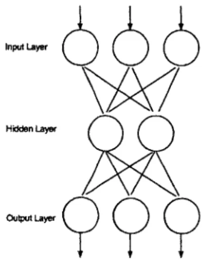
In order to create a computational system, these artificial neurons must be con-nected into a network [4]. A typical network might look something like figure 1-2. The example system has three inputs that are taken in by three input neurons. Since these are input neurons, they just forward the input value. The forwarded values are weighted by the hidden layer synapses and each hidden layer neuron has three weighted inputs to sum. Then the hidden layer neurons threshold the sums and out-put those signals to the synapse of each outout-put neuron. The hidden layer outout-puts are weighted by the output layer synapses and the output neurons each receive two weighted values. Then, each sum is thresholded for the last time, and those values are the three system output values. Of course it becomes more and more complicated as
hidden layers and inputs are added. Eventually, with enough of each, extremely com-plex functions may be approximated, where their accuracy increases as the hidden layers and inputs do. However, the input and hidden layers are not the determining factor for the function emulated by the neural network. The adaptable characteristic of a neural network is the weights. Each neural network is trained by an algorithm to determine the weighting values. Depending on the function to be approximated or purposed of the neural network, the weightings will be very different. For example, if the neural network is for image pattern recognition, then the weights are valued to make the network output the same value for the same patterns, regardless of whether the overall image is the same or not. This is discussed further in Section 2.5.
Input Layer
Hidden Layer
Output Layer
Figure 1-2: Three layer neural network with three inputs, one hidden layer, and three outputs. Image taken from [1].
Despite the exponential growth of microprocessor speed in recent history, tradi-tional systems have been unable to replicate one of the key advantages for neural networks, parallelization. Most artificial neural network processing systems are just neural algorithms running on sequential processors. These software systems attempt simulating parallel environments on sequential devices, resulting in sub-optimal per-formance. Many past attempts to create electrical or electro-optic hybrid parallel physical neural networks have ended prematurely with hardware limitations that rel-egated processing to the sequential realm. The sheer number of interconnections required for larger systems and the number of necessary components for total parallel
processing makes system development a daunting task. This is not even including the design considerations required for an optical or electro-optic hybrid neural net-work. Yet, research continues due to the optimization advantage neural algorithms on hardware hold over standard software in areas such as image processing and pattern recognition [5].
1.2
Project Background
The HENN combines optical neuron connection layers with electronic signal process-ing in a parallel manner. The basis for this project lies in the theory and research for a Compact Optoelectronic Neural Coprocessor (CONCOP)[1]. It was further fleshed out by the first attempts at fabricating optoelectronic components for the CONCOP [6]. The HENN is a prototype precursor to the Compact Optoelectronic Integrated Neuroprocessor (COIN), the evolved successor of the CONCOP. The HENN aims to provide valuable guidance on system design, highlighting problems that need to be solved for the implementation of the COIN. It also provides crucial experience with current and new training algorithms. Ultimately, the goal is to create a fully-functioning prototype that can be a proof of concept. This proof of concept will hopefully generate industry and scientific interest in the COIN project and inspire fabrication and function research of a more industry viable product. The group's current neural system is bulky, immobile, and sequential, as it is the combination of a PC, neuron fiber-optic interconnection plate, and low-grade web camera. The final version of the new HENN system should be somewhat mobile, completely parallel, and capable of performing simple facial recognition, in order to be considered suc-cessful. If this is achieved, the prototype will also open the door for the scientific community at large, as a majority of the work in this field has been on the theoretical and algorithms side, as opposed to the physical.
Chapter 2
The HENN System Architecture
2.1
Defining the HENN System
Unit Architecture
A fully operational HENN system is based directly on the multi-layer neural network model. It is comprised of multiple unit architectures that represent the hidden layers plus separate architectures for the input and output neuron layers. The first step to understanding this, is reviewing the HENN hardware representation of an artificial neuron hidden layer that is part of a larger multi-layer neural network. This sin-gle neuron layer is broken down into five segments: weighting, synapses, summing, thresholding, and outputs and the subsystems that comprise the HENN unit archi-tecture cover one or more of these segments. The list below provides a quick overview of each neuron layer element and the corresponding HENN subsystem
1. Weighting - LCD without backlight 3. Summing -BOD photodetector array 2. Synapses - Fiber optic interconnection 4. Thresholding -BOD comparator array
plate 5. Output - BOD LED array
The neuron layer weighting is represented by an LCD with no backlight (essentially a spatial light modulator) and the synapses are physically manifested by a fiber optic interconnection plate. The last three segments are covered by the bistable optical
Hidden Layer
_
04_
Input Layer Output Layer
Figure 2-1: This three layer neural network outlines the different partitions of the neural network for each type of layer. The partitions serve as a basis for which HENN subsystems are used for each layer.
device (BOD). The BOD is an optical switch that is composed of a photodetector ar-ray, comparator arar-ray, and LED array. The summing of weighted inputs is performed by a phototodetector array. Intensity of the light that has propagated through the LCD and fiber optic interconnection plate sums on the surface of each photodetector. The currents resulting from the measured intensities are thresholded by an array of switch circuits. Each switch either completes the circuit and illuminates a single LED within the neuron layer output LED array or fails to reach threshold and turns its corresponding LED off.
Input and Output Neuron Layer Architectures
With the hidden layer architecture explained, the next step is defining the input and output neuron layers. The input and output layers, in terms of neurons, are best visualized by Figure 2-1. The figure also properly describes the hidden layer as well, and can be used as reference. The input layer simply forwards the input values to the hidden layers and the output layer takes the hidden layer outputs and forwards them out of the system. The output neuron layer is simply a hidden layer that also captures the output image at the end. The most likely candidate for that is a charge coupled device (CCD) camera that records the image and then sends it to the microcontroller
Theoretical Three Layer HENN
Input Layer
Hidden Layer 1
Output Layer
BOD BODBOD
r H for OL
Fiber Ct para or t nterconec.on Comarator opF er uc lar one
Interconnection [.Array LED Plate KArrayv LED Intercnnection KArray LED
Plate Photodetector Array Photodetector Array Plate Photodetector Array
Array r- Array Array
Microcontroller a
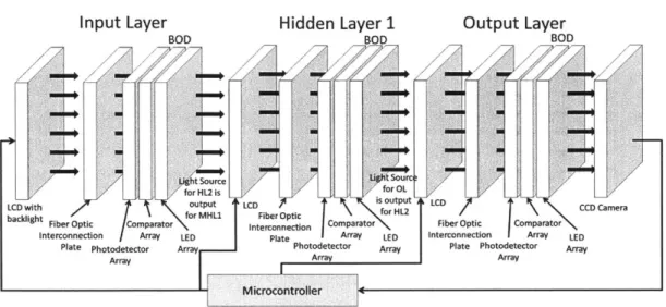
Figure 2-2: Diagram of the theoretical four layer HENN. The black arrows represent prop-agating light and the layers without light communicate electrically.
or computer that helps run the HENN system. The output neuron layer concept will not be explored beyond this as it is not pertinent to this thesis. On the other hand, the input neuron layer, while much simpler, is more critical to this thesis. The input neuron layer itself is just a regular unit architecture layer except it has an LCD with backlight. The input layer receives a weighting image from the master microntroller or computer and then displays that image on the screen.
The input neuron layer is especially important because it is one of the systems on which this thesis focuses. The thesis analyzes an LCD with a backlight and character-izes its attributes. Once that is completed, it determines how well it integrates with the fiber plate. Lastly, a program that displays the connection weights on the LCD is implemented in the thesis. All three of these sections are crucial to the function of the input neuron layer, which is exactly why one of the points of this thesis is to show how an LCD can be used as an input neuron layer.
Operation Overview of a Theoretical Four Layer HENN
Figure 2-2 depicts the complete HENN architecture for a four layer system:
2. Hidden Neuron Layer 1 3. Output Neuron Layer
For this description of operation it is assumed that this is a one-iteration system. However, in actuality this is very far from the truth. While training, the system must iterate and adjust the weights during each training cycle until the desired output on CCD camera is achieved. The input weight image from the microcontroller or computer is written onto the Input Neuron Layer LCD with backlight. The light travels from the backlight through the LCD and is attenuated by the pixels. These pixels modulate the light for each neuron and are controlled by preset weights from the microcontroller. The fiber optic interconnection plate, in the Input Neuron layer, receives the attenuated light and transfers the weighted light to whichever the neurons the synapses have determined. This light intensity is received by the Input Neuron Layer BOD photodiode array, which translates the intensity of each neuron into a current to determine if the neuron's state is on or off. The current is changed to a voltage and sent through the BOD comparator/optical switch, which outputs either high or low voltage. The resulting voltage from each of the neuron's comparators is attached to the BOD output light source (LED Array), which generates an output based on the voltages. The iteration continues onto Hidden Neuron Layer 1, where the LED output light from the Input Neuron Layer is the light source that propagates through the LCD. The LCD weighting is uploaded by the microcontroller and depends on the system training. The modulated light from the LCD couples into the fiber optic interconnection plate. There the HENN operates in the remaining part of the Output Neuron Layer as it did in the Input Neuron Layer. Once the light reaches the BOD output LED array in the Output Neuron Layer, the CCD camera captures the image and sends it to the microcontroller.
The following sections fully explain each subsystem of the HENN unit architecture and the HENN weighting and training.
2.2
Fiber Optic Interconnection Plate
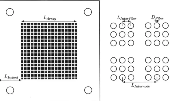
The fiber optic interconnection plate, hereafter known as the fiber plate, is the crux of the project because it allows the system computation to be determined by the simple weighting and summing of light sent through numerous interconnections, rather than a processor. Each neuron acts in parallel with the others and allows for faster compu-tation with little to no power consumption. As the number of neurons increases, so does the parallelization and computing power. The fiber plate connects two layers of neurons with optical fibers. The first neuron layer is a 17 x 17 array of neuron nodes (often referred to as just nodes or neurons), which are groupings of individual fibers. Figure 2-3 provides an excellent illustration of the layout of the fiber plate's first layer. Each inner neuron is a group of nine DFiber diameter fibers that are spaced
Linterfiber apart center to center. The outer neurons are groups of 2 x 3 with the
exception of the corners with are 2 x 2, both have the same spacings as the inner neurons. The reason these edge neurons have less fibers is from the nearest neighbor connection model, which is discussed later in the section. However, the basic idea is the edge neurons have less than nine neighbors, they only have 6 or 4. There is also a
set Llnternode distance from the origin of the center fiber in one neuron, to the origin
of the center fiber in the adjacent neuron. The total length of the active fiber plate area is LArray = (Nodes - 1) -Llnternode + DFiber. The distance from the edge of first fiber plate layer to the center of the first fiber hole is LIndent.
The second layer of the fiber plate has the same dimensions and indent as the first, but with a slight node difference. It still has 17 x 17 nodes, each separated by the distance Llnternode, however, each node is one larger hole of diameter DNode
rather than a square grouping of 3 x 3. Each second layer neuron hole is centered at the origin of the center fiber in the equivalent first layer node. The nine fibers for each second layer node are all situated inside this larger neuron hole, this hole will be positioned right above the detctor which will sum the light coming from the fibers. Figure 2-4 depicts the layout of the second fiber plate layer and the positioning of the fibers in a single neuron node.
L Array 0 U=W=W==W======= NNOUNNNNU======ONN NEW==N-====NNO==N NO===NNONNOME=ONN .=...
INN===ON=OM====ON
IEENNEOUNNO==MONS NOWNEWE=NNE=NNNON INNO===========EM ... INNONNOUNOM=ON=NI NEENNO==E=EENNUMN NO====O====NNOWEN LInter fiber00
00
0
0
0
00
00
00 00
LInternoyjeD
D
D
0
0
0
Figure 2-3: Left: Scaled 17 x 17 node array fiber plate first layer. Right: Zoomed in 2 x 2 node array to illustrate sizing.
The fiber type used for interconnections is an unjacketed plastic optical fiber that has a double concentric structure consisting of a polymethylmethcrylate (PMMA) core and a fluorinated polymer cladding. The high core refractive index and low cladding refractive index means the fiber employs total internal reflection to propa-gate signals. The core and cladding diameters from the manufacturer are listed in Table 2.1.
Table 2.1: Dimensions for three different fiber diameters.
In order to connect the two layers, the design employs nearest neighbor connections for the fibers of each neuron. Each fiber in a node of the first layer would connect
0
0
0
0
0
0
Diameter Layer Avg [iim] Min [pm] Max [pm]
.5 mm core 485 455 515 cladding 500 470 530 .75 mm core 735 690 780 cladding 750 705 795 1 mm core 980 920 1040 cladding 1000 940 1060 Dgiber 40
0
0
o
0ooooooooooooooooo
ooooooooooooooooo
ooooooooooooooooo
ooooooooooooooooo
Qoooooooooooooooo
ooooooooooooooooo
oooooooooooooooo
ooooooooooooooooo
ooooooooooooooooo
ooooooooooooooooo
ooooooooooooooooo
ooooooooooooooooo
ooooooooooooooooo
ooooooooooooooooo
ooooooooooooooooo
00000000000000000ooooooooooooooooo
o
00000000
0
DFiberFigure 2-4: Left: Scaled 17 x 17 node array fiber plate second layer. Right: Zoomed in 2 x 2 node array to illustrate sizing and ideal positioning of fibers.
to one adjacent node in the second layer. Those nodes are determined by using the nearest neighbor principle. The central hole in the layer one node connects to the equivalent node in layer two. The other eight holes in the layer one node, connect to the eight unique nodes closest to the central layer two node. A diagram illustrating this concept is shown in Figure 2-5. This unique connection model allows information to propagate perpendicular to the overall system flow. The values for the current machined fiber plate are in Table 2.2.
Table 2.2: Dimensions for current machined fiber plate.
DNode Measurement Value Dimensions 88 x 88 mm Nodes 17 x 17 DFiber .5 mm LInterfiber .75 mm LInternode 3 mm LArray 48.5 mm Llndent 20 mm DNode 2 mm
1 2 3
G G@
0 4 (D 607 8 9
Figure 2-5: Left: One node on the input side. Right: Nine nodes on the output side. Diagram for the Nearest Neighbor connection model employed in the HENN fiber plate architecture. The left grouping is a single node in the first/input layer of the fiber plate and the right grouping is the nine nearest nodes in layer 2 to the single node in layer one. Each smaller circle represents a single fiber and circles with the same number are the beginning and end of the same fiber.
The fiber plate operates by each node in the first layer receiving attenuated light from the corresponding LCD pixel area. This light then propagates through the fibers via nearest neighbor connections to the nodes in the second layer.
2.3
LCD as a Spatial Light Modulator
The LCDs in the hidden layers, function as connection weights that modulate the light input to the fiber optic interconnection plates. The light traveling from the source passes through the LCD screen on its way to the fiber plate input. If the pixels on the screen are darkened, then the light signal is attenuated after passing through the LCD. In this way, the connections are weighted. As stated in the previous section, the fiber plate input layer has 17 x 17 nodes that are each made of 3 x 3 groupings of fibers. In the HENN project, the weightings are per fiber, so each individual fiber has its own weight. Since each fiber has its own weight and shaded pixels are the source of that weight, then specific pixels should correlate to a specific fiber. Multiple pixels are needed to fully weight an individual fiber and each should have an equal number of pixels. The number of pixels per fiber is based on the positioning of the fiber plate over the LCD and the size of the pixels.
In general, a more sensitive weighting scheme, allows for higher precision of image identification. The variation in intensity attenuation depends on both the number of unique pixel shades for the LCD and the amount of attenuation achieved by each value. For more information on the weighting refer to Section 2.5.
Note that this is not the system tested by this thesis. The experiments were conducted with the backlight, therefore, the conclusions may not be applicable to a spatial light modulator. The light source for the SLM is the output of the bistable optical device. Therefore, as previously explained, the input light has some lights on and others off, compared to the constant on state of the backlight. While uniformity allows for easier characterization and measurement of the LCD capabilities, the results are inconclusive for determining the SLM functionality. However, the characteristics of an LCD serving as a weighting system or input neuron layer are explored in much greater detail starting in Chapter 3.
CA T3:14l-1. 0.,- 1 T
The Bistable Optical Device (BOD) is one of the most challenging segments as an inexpensive reliable electro-optical switch has never been characterized. Therefore, this document will only briefly touch upon one of the possible designs. The BOD is the physical structure for the intensity summing, voltage thresholding, and hidden layer output light source. It is composed of a photo-sensitive element, a transistor switch, and an LED. The BOD's purpose is as an optical switch that will only illuminate an output node if the intensity of the input node is high enough. Figure 2-6 provides a potential circuit schematic candidate for the individual element that will make up the larger array of switches, with one switch per neural node. Using this potential schematic the BOD array would be a photoresistor array, thresholding circuitry array, and a LED array.
For an individual element, the light from the second fiber plate layer creates an intensity pattern on the photoresistor. This incident intensity correlates to a specific resistance, which results in a voltage divider dependent on incident light intensity.
V. RI Photores istor 7
A
LED Amp MOSFET R2Figure 2-6: Potential BOD Circuit with Photoresistor.
The output voltage of this divider sets the gate voltage of a MOSFET and, if that voltage is high enough, then the switch closes and illuminates the LED. BOD research is still ongoing in the group and the final implementation is undecided.
BOD Considerations
The main concern about this layer is the number of discrete components. The plan is to create an array of BODs, one for each neuron, so that the parallel processing can be maintained. The goal is also to create a prototype that is relatively small and com-pact, therefore, the discrete component array may be troublesome. Fortunately, the problem can be solved with integrated circuits, however, that is a more expensive al-ternative to be explored only if necessary. When the photodetector array is flush with the fiber plate, it is important to note the possibility that an individual photodetector element may measure light leakage from neighboring nodes. A preventative measure such as a plastic isolator that fits between the fiber plate and photodetector array, can separate the nodes and completely prevent neighbor light leakage. However, the specific material would require in depth investigation to determine the effects of light absorption and reflection on the perceived intensity by the photodetector. Another concern is the photosensor's range of measurable intensity. Extremely high incident intensities can saturate the sensor, reducing the effective operation range. Similarly, extremely low intensities, may not register on the sensor, also reducing the effective
operation range. Therefore, choosing the proper photosensor is critical for proper operation.
2.5
Training Algorithm and Weighting System
Ideally, the training algorithm will operate in situ or on the HENN hardware. This means that the weighting image is created by the training and the image is generated iteration by iteration. A major benefit to this type of training is that it can accom-modate for inherent system flaws and inefficiencies, because the training algorithm is operating on the actual network hardware. One example is misalignment of the
LCD and fiber plate, the system considers that part of the training, factoring out any losses it might cause.
While current access to in situ training would be ideal for this project, the reality is that it is just a theoretical desire for the system. The actual HENN system in the lab is composed of an LCD, fiber plate, and a USB port for uploading the weights. The reality of the situation and the testing requirements temporarily forces the training and weights algorithm away from in situ and to a manual USB upload. What was once not even a concern for the in situ is now a problem. The only way to upload weights is to the determine their value and then map the 49 x 49 weight array to an image the size the fiber plate active area. This weighting image chapter thoroughly outlines the program to achieve this.
The current training algorithm is what enables the weighting system to exist. It is several different things, but the main idea is that it functions as a system to ensure that the neuron layer weights are properly applied to the fiber connections and that the light is weighted and efficiently propagates through the system to the next layer. Since the LCD tested by the thesis still contained the backlight, then the weighting system best applies to the input neuron layer. It is something that couples light into fibers efficiently, has minimal transmittance loss, is used to display a weighting image on, and has a small amount of variation between fiber light intensities. Those are the characteristics of a weighting system for the HENN architecture with the non-ideal
training algorithm. These are characteristics that are tested in the next chapters and are the source of proof for using an LCD as a weighting system at the input neuron layer.
Chapter 3
Characterizing the LCD
Now that the HENN project has been provided with context and the separate sub-systems explained, the attention can shift to the LCD weighting subsystem where the majority of research was focused. Recalling the goals from the introduction, the thesis will provide the HENN with a usable LCD weighting system and suggestions to improve its integration with the HENN project. Development of a viable LCD weighting system requires several steps to meet the reliability and integration re-quired by the HENN. The first is the characterization of the LCD, a precursory step to set up guidelines for selecting a specific LCD. Once selected, the commercial LCD is tested to determine various screen properties. This chapter attempts to satisfy the LCD guidelines with a commercial LCD and perform a thorough analysis on the se-lected model. It will perform a system physical or practicality assessment, individual pixel analysis, and a spectrum profile measurement. The data gathered from these evaluations will then guide the experiments performed in later chapters.
3.1
LCD Specifications
One of the goals was to avoid buying a commercial spatial light modulator. Therefore, it was necessary to find an LCD screen that could be properly disassembled and used as a transmissive LCD filter with and without a backlight. The experiments for this thesis were done with the backlight in place (suitable for the HENN input layer), and
further experiments are required to draw any conclusions about the LCD as a SLM for the hidden layers. Choosing a screen size was based on the current fiber plate dimensions. The fiber plate connection fiber diameter dictated the screen resolution and active diplay area. With those two values the average pixel size could be calcu-lated and used as a guidelines since more than one pixel per fiber area was required. Additionally, the system required the ability to effectively display weighting images and easily interface with a computer or microcontroller. To meet these demands, the Aluratek ADPF08SF digital picture frame was selected for the first LCD weighting system prototype. Its specifications are in Table 3.1.
LCD Specification Value
Model Aluratek ADPF08SF
Resolution 800 x 600 pixels
Active Screen Width 16.2 cm
Active Screen Height 12.1 cm
Average Pixel Size .2025 mm x .2017 mm
Table 3.1: LCD Specifications
The Aluratek ADPF08SF is a digital picture frame with a plastic shell that holds a metal casing and a controller board that receives button, USB, and power input, which it then relays to the LCD and backlight. The metal casing contains a cold cathode fluorescent light (CCFL), two light diffusers, and the LCD screen secured by a machined piece of plastic. The LCD screen has a 16.4 x 12.3 cm surface with an active display area of 16.2 x 12.1 cm. This allows ample coverage of the 50 x 50 mm fiber plate active area and an average pixel size of less than the required .25 mm. While the ADPF08SF does not directly interface with a computer, it does have a USB port for memory sticks. Therefore, the appropriate weighting image may be loaded onto the memory stick and then inserted into the picture frame, immediately displaying the stored image. The metal casing can be pried open and the CCFL backlight removed, an example of the separated LCD panel is shown in Figure 3-1. This allows the LCD to act as the first HENN light source/weighting filter with the backlight or as a thin weighting filter between an LED array and a fiber plate in the
middle stages of the system.
Figure 3-1: Separated LCD panel from the Aluratek ADPF08SF digital picture frame.
For placement between an LED array and fiber plate, the LCD panel must exist with no backlight. The removed backlight leaves a large amount of space within the metal casing, but the machined plastic piece still holds the LCD panel in place without extra reinforcement. To create the desired transmissive spatial light modulator, there must be a hole in the back of the metal casing. Ideally, the LED array would fit into the backlight hole. The adaptability of the Aluratek system is one of the main reasons it successfully met the requirements. Its systems were simple and functional, which provided room for the further modification required by future experiments.
3.2
LCD Pixel Analysis
Liquid crystal displays use the RGB color model to display color. The pixels that compose the screen are further broken down into three sub-pixels with color filters, red, green, and blue. Up close, the individual sub-pixels are discernible, but at a viewing distance, the separate sources are indistinguishable. The images displayed on the LCD can be represented as an array of pixels when stored in memory. Using this representation, pixels are structured similarly to their physical counterparts, a grouping of three binary values ranging from 0 to 255 base ten. Each value represents the amount of red, blue, or green present in the pixel color. Grayscale values occur
when all three values are equivalent, starting with black (0,0,0) and ending with white (255,255,255). There is also area between the pixels themselves, called dead space. It does not contribute any intensity, but affects the intensity input to any smaller object. To measure the pixels and this dead space, the LCD screen was placed under a microscope and sized according to the eyepiece reticule units. Figure 3-2 is two images of different display patterns captured by the microscope.
Figure 3-2: Two microscope pictures of the LCD pixels from the Aluratek ADPF08SF. The left is when all pixels are on and white, while the right is a black and white checkerboard pattern. Wdead Wpjei = WR + WG + WB WR WG WB Wpxel+ R G B R G B
t
Hdead R G B R G BFigure 3-3: On the left: the Red Green Blue composition and sizing of a single LCD pixel. On the right: Sizing of the dead spaces between pixels for the chosen LCD screen.
In order to find the metric equivalents to the measured unit values in Table 3.2, the pixel spacing must be determined. Using the pixel layout illustrated in Figure 3-3
Measurement Name Variable Value [Units] Value [pm]
Pixel Width Wpixel 10.25 184
Pixel Height Hpixei 7.75 139
Sub-Pixel Width WR = WG = WB 3.41667 61.333
Dead Width
Wdead1.0
18
Dead Height
Hdead3.5
63
Table 3.2: Pixel Size and Spacing Measurement Data
and assuming that there is no dead space between the edge of the screen and the edge pixels, a single row can be described by the summation of pixel widths and dead spaces. The same applies for a single column.
Lro = 800 Wpixei + 799 Wead = 162 mm
(3.1)
Leol = 600. Hpixei + 599 - Hdead = 123 mm
With these equations and the ratios of dead space and pixels to total units, the value for a single unit can be calculated. After performing the computations, the value for 1 Unit is:
1 Unit = .0179 mm (3.2)
With the result of Equation 3.2, the unit values in Table 3.2 may be transformed to metric values.
3.3
LCD Spectrographic Analysis
In order to measure the absolute intensity of a specific light source, it is necessary to know its wavelength intensity profile. The intensity Ee (A) of a single frequency light wave incident on a given surface (also called irradiance) is described approximately by Equation 3.3, where E is the complex electric field amplitude, n (A) is the refractive index of a medium based on a given wavelength, co is the speed of light in a vacuum,
and Eo is the vacuum permittivity [7].
Ee (A) ~ n (A) COEO E 2 (3.3)
2
While the most precise answer would involve calculating the LCD output irradi-ance for each wavelength, equipment and time constraints eliminate the feasibility of this approach. Fortunately, most light sources can be characterized by a small number of peak intensity wavelengths with narrow bandwidths. An accurate esti-mate of intensity can be calculated by summing the intensity values of these peak wavelengths.
The wavelength distribution for the LCD is determined by the CCFL spectrum and the wavelength absorption of the sub-pixel color filters. The wavelength intensity profile is measured with a grating spectrometer, which passes light from the source through the diffraction grating, which splits and diffracts light, which is captured by a digital camera. The digital camera image is parsed into a MATLAB program that measures the relative intensity of light for each frequency and creates a wavelength intensity profile.
Based on the pixel information in Section 3.2, the color white is created when all three sub-pixels are fully illuminated. This suggests that the white intensity profile should be the sum of the blue, green, and red intensity profiles. However, this does not help determine the wavelength or intensity contributed by each color, since the sub-pixel blue may contain green wavelengths and vice versa. The best method is to illuminate and measure each sub-pixel separately and then all together as white. So for each color, the LCD screen was illuminated with only one of the three sub-pixels, except for white which required all three.
The precision required for obtaining the peak wavelengths for each color and white was not very high. The purpose was to obtain average wavelengths and relative in-tensities. The relative intensities helped determine the relative intensity distribution for each color in white and the average wavelengths were used to find the absolute power of each color using another instrument. The spectrometer system had to be
Red Spectrum 14 12 - 10-8 6 -4 2 400 450 500 550 600 650 700 Wavelength (nm) Blue Spectrum 20 .E10 5 Green Spectrum -0 5 0 5 00 450 500 550 Wavelength (nm) White Spectrum 600 650 700 12 10 8 4 2 400 450 500 550 600 Wavelength (nm) 650 30 25 20 15 10 5 700 o00 450
Figure 3-4: Spectra of the LCD screen when all pixels are
WI>
-600 50 60 65 70
500 550 600 650 700
Wavelength (nm)
Red, Green, Blue, or White.
calibrated with a fluorescent light to determine the location of specific colors and had a resolution of .41 nm/pixel and an experimental error of t4.509 nm. In order to val-idate these results, it is assumed that the web camera is approximately equi-sensitive to all experimentally measured wavelengths. Additionally, the input intensity of the measured LCD screen is assumed sufficient for proper spectrum calculation and cali-bration. The average wavelength for red and green are easily determined by examining their peaks in Figure 3-4. For blue, the selected wavelength is a weighted average of the two peak wavelengths to simplify calculations. The two peaks for blue are 453 nm and 519 nm. The relative intensities RI1 and RI2 are 8.75 and 13.76 respectively.
A = Aj.R 1j+ARI2, provides the weighted average wavelength for blue. The selected
average wavelengths for each color are listed in Table 3.3.
KJ\J\p\
1\Kn
Color Selected Wavelength A [nm]
Red 584
Green 537
Blue 493
Table 3.3: Selected Wavelengths for each color on the LCD
3.4
Absolute Intensity and Pixel RGB Values
The spectrometer provided the relative intensity in arbitrary units, however, to de-termine the light coupling efficiency from the LCD to the fibers, fiber losses, and the intensity of a single pixel, the absolute intensity is required. The absolute intensity can be measured using a silicon power sensor and the LCD screen. The sensor op-erates by generating a specific current proportional to the incident intensity. Since the sensor cannot determine the intensity wavelength, the intensity-current propor-tionality constant varies with the wavelength. Before the measurement is taken, the assumed wavelength is input, selecting the constant and, therefore, determining the absolute intensity. It was for this reason that the spectrum analysis was performed and the average wavelength per color, shown in Table 3.3, was selected. For the measurement, an apparatus was constructed to secure the LCD screen position and prevent movement. To account the illumination of the entire LCD for each data point, a piece of black construction paper with a 20 x 20 mm square cut out was taped onto the LCD. Then the power sensor origin was aligned with the center of the square, placed flush against LCD/paper and locked into place. The square cut out was slightly larger than the 1 cm2 active area of the circular sensor. This ensured
that any measurement of intensity was in terms of pW/cm2
, which can be used to
calculate incident intensity for other input areas. To determine the variation of each color's intensity over the entire range of 0 to 255 with acceptable precision, a data point was collected every eight values, so R, G, or B = [0,8,16,...,240,248] and then also at the value maximum, 255. The resulting intensity measurements and their trends are displayed in Figure 3-5. As a precaution, the environmental intensity (in-tensity of LCD with backlight off) was measured at 0 picoWatts. However, the power
sensor has a resolution of 100 pW, so it was guaranteed less than that and therefore negligible to this measurement.
Relative Intensity of RGB Values Blue (486 nm) 0.9 - ---- Green (537nr) . -. -.-.. -.--.- ..-- -.. - - Red (584 nrn) 07 0.2 -- - - - -- -0 50 100 150 200 250 (RGB) Value
Figure 3-5: Peak Wavelength for each color on the LCD
The results show a clear trend correlating to increasing intensity with increasing R,G, or B value. More specifically, the change in intensity AI increases as the R, G, or B value increases, creating a nonlinear relationship. Despite the color specificity of the data, it is reasonable to infer the same relationship for mixed RGB values as well, specifically, the gray scale. However, the accuracy of this exact nonlinear relationship is only guaranteed for the backlight LCD combination, and may not be a valid observation in all cases. The experiment was performed using a backlight and LCD that were fabricated to function as a single unit, compensating for the others weaknesses. Despite this, generally, it is safe to assume that for any light source, varying the RGB value, will produce a result where transmitted intensity is directly proportional to RGB value. This attenuation can be attributed wholly to the LCD as the backlight illuminates the entire LCD with a uniform intensity. If this were not the case, then it be impossible to display multiple color shades on the screen at a time.
The key implication from these results is the validation of using an LCD to modu-late the light intensity for the input neuron layer. Spatial light modulators attenuate the light that propagates through them and the LCD could not act as one if it was unable to do this. The LCD generates a range of unique intensities with correspond-ing RGB values adequate for neural network weightcorrespond-ing. With this evidence, it is
Color
A [nm]
Abs
Imax [pW/Cm2]Red 584 7.077
Green 537 10.21
feasible to imagine a weighting image that applies different attenuation to different RGB values and is mapped to align with the fiber plate input fibers. This software based weighting image would turn the LCD into a reprogrammable and size adapt-able connection weighting system. The software development is discussed further in Chapter 5. The only caveat that must be considered for neural network adequacy is selecting a photoelement with the correct measurement range and sensitivity. This validation of neural network adequacy applies to any combination of LCD and light source, but the relationship plotted in Figure 3-5 does not. More investigation is needed to construct the exact RGB relations for other lighting sources, such as LEDs and OLEDs.
Chapter 4
Interfacing the Fiber Plate and
LCD
The previous chapter on LCD Characterization performed a base characterization and investigation of the LCD system and how it functions. These preliminary ac-tions were necessary in order to determine the proper experiments for more in depth characterization and to discover specifications needed to perform more experiments. Comprehensive characterization of the LCD screen for the purposes of the HENN project required several intensity tests be conducted. This chapter will cover each of the experiments in detail, including their purpose, procedure, results, and impact on the HENN's evolution.
4.1
Position-based Variation of Fiber Input Light
Intensity
Purpose
One of the largest concerns with employing an LCD screen was the existence of dead spaces between the rows and columns of pixels. Due to the small fiber diameter used for the fiber plate interconnects, it was suggested that the positioning of the fiber over the LCD would have a non-negligible effect on input intensity. Therefore, it was
![Figure 1-1: Basic neuron model with four inputs. Image taken from [1].](https://thumb-eu.123doks.com/thumbv2/123doknet/13855740.445113/19.918.336.562.534.687/figure-basic-neuron-model-inputs-image-taken.webp)