HAL Id: hal-01763540
https://hal.archives-ouvertes.fr/hal-01763540
Submitted on 14 Dec 2020
HAL is a multi-disciplinary open access
archive for the deposit and dissemination of
sci-entific research documents, whether they are
pub-lished or not. The documents may come from
teaching and research institutions in France or
abroad, or from public or private research centers.
L’archive ouverte pluridisciplinaire HAL, est
destinée au dépôt et à la diffusion de documents
scientifiques de niveau recherche, publiés ou non,
émanant des établissements d’enseignement et de
recherche français ou étrangers, des laboratoires
publics ou privés.
Control the Transport of Injected Charges in Thin
Dielectrics
K Makasheva, Christina Villeneuve-Faure, Caroline Bonafos, Christian
Laurent, Alessandro Pugliara, Bernard Despax, Laurent Boudou, G. Teyssedre
To cite this version:
K Makasheva, Christina Villeneuve-Faure, Caroline Bonafos, Christian Laurent, Alessandro Pugliara,
et al.. Dielectric Engineering of Nanostructured Layers to Control the Transport of Injected Charges
in Thin Dielectrics. IEEE Transactions on Nanotechnology, Institute of Electrical and Electronics
Engineers, 2016, 15 (6), pp.839-848. �10.1109/TNANO.2016.2553179�. �hal-01763540�
Abstract1—New concept concerning dielectric engineering is
presented in this work aiming at a net improvement of the performance of dielectric layers in RF MEMS capacitive switches with electrostatic actuation and an increase of their reliability. Instead of synthesis of new dielectric materials we have developed a new class of dielectric layers that gain their performance from design rather than from composition. Two kinds of nanostructured dielectrics are presented. They consist of: (i) silicon oxynitride layers (SiOxNy:H) with gradual variation
of their properties (discrete or continuous), and (ii) organosilicon (SiOxCy:H) and/or silica (SiO2) layers with tailored interfaces; a
single layer of silver nanoparticles (AgNPs) is embedded in the vicinity of the dielectric free surface. The nanostructured dielectric layers were deposited in a plasma process. They were structurally characterized and tested under electrical stress and environmental conditions typical for RF MEMS operation. The charge injection and decay dynamics were probed by Kelvin Force Microscopy (KFM). Modulation of the conductive properties of the nanostructured layers over 7 orders of magnitude is achieved. Compared to dielectric mono-layers, the nanostructured ones exhibit much shorter charge retention times. They appear to be promising candidates for implementation in RF MEMS capacitive switches with electrostatic actuation, and more generally for applications where surface charging must be avoided.
Index Terms—silver nanoparticles, silicon nanoparticles, nanostructured dielectric layers, plasma processes, MEMS.
I. INTRODUCTION
HE electrostatic charging of thin dielectric layers represents an intensive field of scientific research due to
1 Manuscript submitted on October 27, 2015. This work was financially supported by Agence Nationale de la Recherche in France, project ANR-InTail under contract ANR-AA-PBLI-II-2011. The authors acknowledge financial support from the French CNRS and CEA METSA network for the TEM observations, project METSA 11B14, experiments performed at the CEMES platform.
K. Makasheva, C. Villeneuve-Faure, C. Laurent, A. Pugliara, B. Despax, L. Boudou and G. Teyssedreare with LAPLACE laboratory, Université de Toulouse, CNRS, UPS, INPT, 118 route de Narbonne, F-31062 Toulouse, France (e-mail: kremena.makasheva@laplace.univ-tlse.fr, christina.villeneuve@laplace.univ-tlse.fr, christian.laurent@laplace.univ-tlse.fr, alessandro.pugliara@laplace.univ-tlse.fr, bernard.despax@laplace.univ-tlse.fr, laurent.boudou@laplace.univ-tlse.fr, gilbert.teyssedre@laplace.univ-tlse.fr).
C. Bonafos and A. Pugliara are with “Nano-optics and nanomaterials for optics” group-CEMES-CNRS, Université de Toulouse, 29 Jeanne Marvig, BP 94347, F-31055 Toulouse, France (e-mail: caroline.bonafos@cemes.fr, alessandro.pugliara@cemes.fr).
the numerous applications of dielectric materials in electrical engineering, yet requiring a comprehensive study. Electrostatic charging of thin dielectric layers is a physical phenomenon simultaneously present at scientific and technological levels. The charge injection in dielectrics is at the origin of space charge formation [1]. The later effect induces modification in the electric field distribution leading in some cases to unexpected behaviour of the dielectric layers under electrical stress and can be considered as a failure route for many technological devices. The mechanisms of charge trapping and charge transport in dielectrics largely depend on the strength and the timescale of the applied electrical stress, on the composition of the dielectric material itself and on its thickness, especially when the layer thickness is of order of few tens of nanometers [2, 3].
Although the electrostatic charging of thin dielectric layers lays down the principle of operation of various technological devices, like non-volatile memories [4, 5] or electret based microphones [6], it is considered as the main cause of electrostatic sticking in MicroElectroMechanical Systems (MEMS) [7] or for the damage of electronic devices due to Electrostatic Discharges (ESD) [8]. Indeed, the dielectric charging in RF MEMS switches is at the origin of failure and low reliability of capacitive switches with electrostatic actuation [9-15]. Charge trapping on the surface and in the volume of the dielectric layer leads to significant increase of the surface potential and to modification of the values of applied voltage for switch actuation in a way that after certain number of events the switch is out of control.
RF MEMS capacitive switches operate at 6 GHz and above due to their relatively small down-state capacitance (2 – 5 pF) [7]. Different dielectric layers have been tested in order to improve the performance of RF MEMS capacitive switches [14, 15]. In general, dielectric layers with high dielectric constant are favored because of the resultant high capacitance ratio between “on” and “off” states of the switch. On the current stage of development of the RF MEMS technology silicon nitride (Si3N4) is the most frequently used dielectric layer because of its relatively high dielectric permittivity
(Si3N4 = 7.5) [16]. However, the defect concentration in Si3N4
is quite high and charge trapping effects are significant. Concerning the aluminum dioxide (Al2O3), it should be pointed out that due to its highly ionic nature, the Al2O3
T
Dielectric Engineering of Nanostructured Layers to
Control the Transport of Injected Charges in Thin
Dielectrics
Kremena Makasheva, Member, IEEE, Christina Villeneuve-Faure, Caroline Bonafos,
Christian Laurent, Fellow, IEEE, Alessandro Pugliara, Bernard Despax,
exhibits ionic, dipolar, and space charge polarizations [17], which disqualify it as dielectric material for RF MEMS even though its dielectric constant is high (Al2O3 = 9.0). Searching for dielectrics with high dielectric constant other materials have also been envisaged for study. Although known as high k materials, hafnium dioxide (HfO2, HfO2 = 25) and tantalum pentoxide (Ta2O5, Ta2O5 = 22) consist mostly of ionic bonds and show high levels of charging. Consequently, these materials are out of scope of the studies on RF MEMS [18].
Finally, silica (SiO2) remains the most appropriate choice in terms of low charge trap level. Yet, its relatively low permittivity (SiO2 = 3.9) reduces the capacitance ratio of the switch directly shrinking the reliability of the switch.
Attempt to face the problem of high density of traps in Si3N4 by introducing e.g. carbon nanotubes (CNTs) in silicon
nitride to form a nanostructured dielectric material with less charging memory was presented in [19]. The resulting material exhibits improved “Figure of Merit” which arises from higher dielectric conductivity when gradually approaching the percolation threshold due to the increased CNT density. More recently, another solution to improve the performance of Si3N4 by modulation of the electrical
properties of gold rods nanostructured silicon nitride was investigated [20]. Nanorods with different diameters (150 and 500 nm) and densities (by varying the inter-nanorods space from 1 to 10 m) were grown in Si3N4 layers and a model
predicting the threshold inter-nanorods spacing to prevent from overlapping the fringing field was implemented to describe both the DC and low frequency electrical properties.
Naturally nanostructured dielectric materials such as nano-crystalline diamond revealed suitable discharging behavior over a wide range of frequencies. Their transport properties and impact on the long-term charging and discharging processes in MEMS capacitive switches have been reported [21]. Focus was also made to ultra-nano-crystalline diamond thin films [22-24]. It was shown that the electrical conductivity from an insulator to practically a semi-metal is depending on the amount of nitrogen incorporated in the ultrathin films [23]. This unique electrical conduction seems to depend as much on the particular grain boundary structure and bonding, including nitrogen incorporation into the grain boundaries, as on the microstructural changes in nitrogen doped films. Carbon based nanomaterials, including one-dimensional CNTs and two-one-dimensional graphene, have also attracted great research interests in the recent years for various potential applications in MEMS/NEMS applications [25]. Following the above discussion, it is obvious that the choice of dielectric layer does not appear straightforward. It requires a new perception in the development of dielectric layers, consistent with the severe requirements for performance and reliability of the RF MEMS capacitive switches.
With this contribution we expand on an earlier paper [26] in which we reported the experimental results on the global response of dielectric layers for RF MEMS capacitive switches by using integral methods for characterization of their electrical properties. The information gathered by
studying Metal/Insulator/Metal (MIM) capacitors as performed earlier is very valuable, offering the possibility to follow the current transient in charging and discharging phases and to conclude that the transient processes are controlled by charge accumulation within the material. However, getting information on the local distribution of charges after injection in the dielectric layers requires diagnostic techniques that apply locally, at nanoscale level, like Atomic Force Microscopy (AFM) in Kelvin Force Microscopy (KFM) mode. Attaining, and further analyzing, the local charge dynamics after injection largely serves improvement of the performance of thin dielectric layers under electrical stress by evolving their response through local changes in the structure of the dielectric layers. This way of development is disclosed in the current paper, offering the possibility to create different kinds of nanostructured dielectric layers by plasma deposition in order to control the charge transport in thin dielectrics. To complete the followed strategy, an original approach to control the transport of injected charges in thin dielectrics by tailoring their surface without modifications in the bulk of the material, which in part was introduced in an earlier presentation [27], is also described. It is based on the idea to cover the dielectric material by a nanocomposite layer consisting of a single layer of silver nanoparticles (AgNPs) embedded in dielectric matrix with well-controlled insulating properties. Due to the ability of AgNPs to store electrical charges they are thought to play the role of permanent deep trapping centers thereby stabilizing the injection process by reduction of the electric field at the injecting electrode when the AgNPs are charged. Accordingly, in this work, we would like to capitalize on the synthesis, structural and electrical characterization at nanoscale level of nanostructured layers to control the charge transport in thin dielectrics. Instead of synthesis of new dielectric materials, we have developed a new class of dielectric layers that gain their performance from design rather than from composition. Regarding the composition of the dielectric layers our choice was to go with silica layers (SiO2) with modulated structural and conductive properties. The presented here nanostructured layers are of two kinds: (i) silicon oxynitride layers (SiOxNy:H) with gradual variation of their properties (discrete or continuous), and (ii) organosilicon (SiOxCy:H) and/or silica layers (SiO2) with tailored interfaces – a single layer of AgNPs is embedded at the vicinity of the dielectric free surface, at a well-controlled distance. The nanostructured dielectric layers were deposited in a Plasma Enhanced Chemical Vapor Deposition (PECVD) processes, fully compatible with the microelectronic technology. They were characterized with various diagnostic methods to obtain information on their structure and composition. Visualization of their in-depth organization was achieved by Transmission Electron Microscopy (TEM). The elaborated nanostructured layers were electrically tested under electrical stress and environmental conditions typical for RF MEMS switches. The charge injection and decay dynamics were probed mainly by KFM. Some of their global parameters, like resistivity and dielectric permittivity of the structures, were drawn by study of MIM’s capacitors.
II. EXPERIMENTAL PART A. Plasma deposition of nanostructured layers
Capacitively coupled radio-frequency (RF) discharges operating at 13.56 MHz and low gas pressure (tens of Pa) were used for deposition of the two kinds of nanostructured layers. According to the structure and composition of the dielectric layers two plasma configurations were employed. A brief description of each plasma process along with discussion on its advantages is given below.
The nanostructured layers with gradual properties (discrete or continuous) are composed of multi-levels of amorphous silicon oxynitride layers (a-SiOxNy:H, x<2, y<1) with different
Si concentration. Thin sub-stoichiometric a-SiOxNy:H layers
were deposited on Si (100) wafers in RF plasma sustained by applied power of 5 W, modulated with square pulses of period T = 400 ms and pulse width of 100 ms [5, 26]. Modulation of the applied RF signal allows better control of the available radical species in the plasma, and of the formation of Si nanoparticles in the discharge in case of Si-rich mixtures, before being deposited. The gas mixture contains SiH4, N2O
and He. The precursor ratio = [N2O]/[SiH4] (partial pressure
ratio) allows adjusting the silicon concentration in the film.
The dielectric layer with = 100 exhibits properties close to a thermal SiO2 layer. The lower the -value, the richer in Si the dielectric layer is. The total gas flow in the discharge was 210 sccm (sccm stands for standard cubic centimeters at
standard temperature and pressure) corresponding to a total gas pressure of p = 65 Pa. The He-component in the mixtures was fixed to 40%. Using He in the gas mixture leads to a higher dissociation degree of the precursor molecules due to the higher mean electron energy in He-plasmas. The substrate temperature was kept to 300°C during the deposition process. The low injected power in the discharge and the increased substrate temperature allow better organization of the matrix of the deposit thus preventing from creation of a large number of structural defects which in the most cases are also traps for electrical charges. Scheme of the two multi-level nanostructures with discrete or continuous gradual variation of their structural and electrical properties is given in Fig. 1.
The difference between discrete and continuous multi-level nanostructures is understood in terms of layer composition gradient. To obtain the discrete nanostructures the plasma is activated once the gas composition is adjusted for the targeted -ratio. It means that the deposition is stopped once a given level is realized to prepare the following -ratio. For the continuous nanostructures, the plasma is uninterruptedly activated and the gas mixture, i.e. the -ratio, is gradually
changed between the deposition of successive levels. Formation of interfaces is thus avoided in the second case.
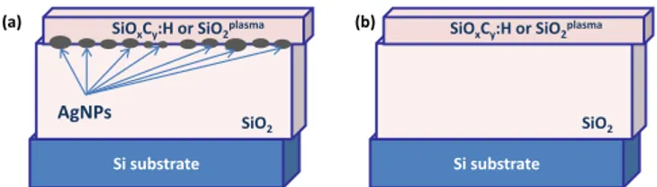
Sketch of the nanostructured dielectric layer with tailored interfaces is shown in Fig. 2a. For evaluation purposes a dielectric layers without AgNPs were also elaborated (Fig. 2b).
To realize this kind of nanostructures a single layer of AgNPs was deposited on thermally grown SiO2 layer on Si substrate in the plasma of axially-asymmetric RF discharge [27, 28]. The discharge powered electrode (smaller electrode) was Ag-made target to bear the silver sputtering. The axially-asymmetric design of that RF discharge induces a self-bias voltage Vdc on the powered electrode controlling in that way the metal sputtering. The plasma was maintained in pure argon at low pressure (p = 5.4 Pa) with RF power of P = 80 W (Vdc = - 1000 V). The sputtering time was fixed to 5 s. The dielectric layers covering the AgNPs of either plasma organosilicon deposit (SiOxCy:H) or plasma silica (SiO2plasma) were obtained in the same reactor with argon-hexamethyldisiloxane (HMDSO, [CH3]6Si2O) mixture for the SiOxCy:H layer and with Ar-HMDSO-O2 mixture for the
SiO2plasma layer at total gas pressures of ptot = 6.6 Pa and
7.7 Pa, and input powers of P = 80 W and 120 W, respectively. A strong originality of this process is the pulsed injection of HMDSO which allows fine tuning of the plasma properties; hence elaboration of high quality plasma silica layers. For both layers the thickness was controlled through the deposition time. More details on the reactor, the plasma process, the deposition procedure, and the plasma input parameters are given elsewhere [27-29].
B. Structural Characterization Methods
Structural characterization of the deposited nanostructured layers was carried out by applying various diagnostic methods. Visualization of the two kinds of nanostructured dielectric layers was achieved by TEM in cross-sectional (XS-TEM) and plane view (PV-TEM). Specimens transparent to electrons have been prepared according to a standard procedure: mechanical polishing and Ar+ ion milling. The observations were performed using a field emission TEM, FEI Tecnai™ F20 microscope operating at 200 kV, equipped with a spherical aberration corrector and the Gatan Imaging Filter (GIF) TRIDIEM. The Fourier Transform Infrared (FTIR) spectra were acquired with a Brucker Vertex 70 spectrometer in the range 400 – 4000 cm-1 to obtain information about the composition of plasma elaborated nanostructured layers. Thicknesses of the nanostructures were determined by spectroscopic ellipsometry using a SOPRA GES-5 ellipsometer in the range 250 – 850 nm.
Fig. 1. Scheme of multi-layer nanostructured dielectrics with: (a) discrete and (b) continuous gradual variation of their properties.
Si substrate 3 2 1 = 5 = 10 = 100 = 25 n (a) Si substrate n 2 1 = 5 = 100 (b)
Fig. 2. Scheme of nanostructured dielectrics: (a) with tailored interfaces by a single layer of AgNPs and (b) without AgNPs.
Si substrate
SiO2
(a)
AgNPs
SiOxCy:H or SiO2plasma (b)
Si substrate
SiO2
C. Electrical characterization procedure
Charge injection and decay mechanisms were studied by AFM in KFM mode by following a specifically developed methodology in order to improve results accuracy and reproducibility [30]. Surface potential measurements were performed by using a Multimode 8 Bruker apparatus. A controlled environment, without humidity and under N2 atmosphere, was applied thus avoiding charge dissipation due to the water film generally formed on the sample surface. PtIr coated Si-tips were used for charge injection and surface potential measurement steps. The charging step was achieved in contact mode (contact force set to 20nN) by applying positive or negative DC bias between ±5V and ±25V to the AFM tip during fixed time, the sample back side being grounded. This provides applied fields of the order 30-150 kV/mm under the tip. However, owing to the divergent configuration and on the strong dependence of the field distribution on the actual tip shape, we keep on referring to the applied voltage when describing the charging conditions by AFM in the following.
After the charging step, the same tip was used to probe the surface potential by Amplitude Modulation KFM with 5nm-lift. Analysis of the obtained results is based on the evolution of the following parameters [30]: Vm – potential maximum of the measured KFM potential profile, related to the applied electric field during charge injection, Full Width at Half-Maximum (FWHM) of the KFM potential profile characterizing surface spreading of the injected charges, and integrated intensity Is – the area under the KFM potential profile, which can be considered proportional to the injected charge density, to monitor the charge dynamic after injection.
To obtain the volume resistivity of the studied dielectric layers we have prepared MIM capacitors. Only for this kind of measurements the nanostructured dielectric layers were deposited on Si-substrates covered by an Au/Ti layer in order to create the MIM device. The Au/Ti layer was evaporated on the Si-substrate and no influence, such as Au-atoms migration, was detected on the plasma deposited layer [30]. To complete the MIM structure a circular golden top electrode of 4 mm in diameter was deposited by sputtering on the surface of the plasma deposited layer, while the ground electrode was the Au/Ti layer [26]. The conduction current measurements were carried out under vacuum (10-3-10-4 Pa) at room temperature.
Under a step DC voltage application between the top electrode and the Au/Ti layer, the current flowing through the volume of the dielectric layers was recorded at different electric fields by a Keithley 617 electrometer. Applied fields were in the range 2-200 kV/mm. The polarization time was fixed to 1000 seconds and was considered as leading to a representative conduction current. After each polarization step the sample was short-circuited for 1000 seconds to recover its initial state. The volume resistivity was calculated from the measured current density vs. electric field curves in their linear region, as reported earlier [26].
III. RESULTS AND DISCUSSION
The dielectric engineering, as performed in this work, allows exploring a large band of operating conditions of the nanostructured layers. For clarity of presentation the two kinds of nanostructures will be discussed separately.
A. Silicon oxynitride layers with gradual properties
Before assembling the nanostructures, the corresponding layers with = 100, 25, 10, 5, and 2 were deposited and characterized singly. The dielectric nanostructures were engineered starting with a high resistivity layer ( = 100 or 25) on bottom. In the following levels the conductivity was increased by increasing the Si-content (i.e. decreasing –value, = 10) to finish the nanostructure with a top level having further increased conductivity ( = 5 or 2). Such design is in accordance with the structure and operation mode of RF MEMS capacitive switches. The highly insulating layer will be in contact with the center conductor in a coplanar waveguide (CPW) configuration and the layer with higher conductivity will face the switch membrane [12]. Thus, the designed nanostructured dielectrics will assure good isolation in the MIM structure avoiding Joule losses of the wave energy during commutation, however, favoring evacuation of deposited charges after each switch actuation, and getting ready the dielectric surface for the next actuation. The apparent dielectric permittivity of the nanostructures will be above the one of thermal silica SiO2 = 3.9 and limited by the permittivity of amorphous silicon a-Si = 12, fulfilling the requirements of high capacitance ratio between “on” and “off” states of the switch. Various a-SiOxNy:H nanostructured layers with gradual properties were deposited.
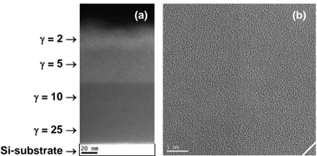
Visualization of the nanostructured layers is achieved by Energy Filtered TEM (EFTEM) in a XS-view, by filtering in the low loss region around the Si plasmon (at 17 eV) associated with Si-nanoparticles [31]. In EFTEM observations all Si-nanoparticles with diameter larger than 1 nm, either amorphous or crystalline, appear as white spots in a dark grey
background (SiOx-matrix). A nanostructure with continuous variation of the properties ( = 25→10→5→2) is shown in Fig. 3. One can observe the appearance of successive a-SiOxNy:H levels with increased Si-content corresponding to increased white contrast. The layers with = 2 and 5 appear Si-rich (Fig. 3a). The ones with = 25 and 10 are slightly distinct due to the identical Si-content (36.0 at%) however with different contributions to the oxidized states of Si, mainly through Si2+ and Si3+ [26]. The High Resolution TEM
(HRTEM) image in XS-view (Fig. 3b) shows that the plasma deposited nanostructured layer is fully amorphous all along the layer depth. The small bottom right crystallized corner represents the crystalline Si-substrate.
Fig. 3. TEM images of a-SiOxNy:H nanostructured layer with continuous
variation of its properties ( = 25→10→5→2): (a) EFTEM image in XS-view, and (b) HRTEM in XS-view.
= 2 = 5 = 10 = 25 Si-substrate (b) (a)
The recorded FTIR spectra of a-SiOxNy:H nanostructured layers exhibit modulated characteristics with input of each -level according to its composition and thickness. The Si-O-Si stretching band at 1023 cm-1 on Fig. 4, mainly determined by the levels with high ( = 100 and 25), is slightly shifted towards higher energies accounting for the increased Si-content in the lower -value levels in the nanostructure [26]. It
envelops the Si-N asymmetric stretching band at 870 cm-1.
The peak is enlarged according to the amorphous nature of the nanostructure. Appearance of a peak at 2253cm-1, associated with the H-SiO3 vibration, reflects the higher Si-content for low -value levels ( = 5 and 2) in the upper part of the nanostructure (Fig. 3a). The presence of Si-H band in the spectrum implies that the nanostructure composition should be written as a-SiOxNy:H to account for the hydrogenation. The features of the FTIR spectrum of nanostructured dielectric layers with continuous levels are identical.
Potential profiles induced by charge injection for 1 min at 25 V in mono-layers with different -values are represented in Fig. 5. They confirm the highly isolating nature of the silicon oxynitride layers with = 100 and 25. The injected charges are
stored on the layer surface, close to the injection point. Although the potential profiles for the Si-rich layers ( = 5 and
2) show injection of charges close to the injection point, the potential maximum is much lower due to charge dissipation into the layer depth. The potential profile of = 10 layer shows a large surface spreading of the injected charges underlying large surface diffusion of the injected charges.
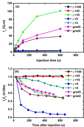
The evolution with charging time of the integrated intensity of potential profiles for bias voltage of 25 V is shown in Fig. 6a for mono-layers with different -values and for two
nanostructured layers with continuous levels
= 100→25105 and = 100, 251052, with total thicknesses of dtot = 173 nm and 188 nm, respectively, called hereafter grad5 and grad2. The same dynamical behavior is observed whatever the amplitude of the applied bias as well as a function of the polarity (positive or negative bias).
It might be tempting to fit the charge decay in time by common laws used in the literature to describe charge relaxation, e.g. as an exponential law, stretched exponential, or hyperbolic law [10, 32]. However, it can readily be judged as not appropriate for the present results. Besides the numerous candidates of physical mechanisms for discharge [32], voltage potential drop resulting from transport of previously injected charges may arise either from lateral spreading or in-depth dissipation of the charge or from following complex kinetics own to the local distribution of the field: geometries involved imply an outright three-dimensional problem due to the small size and nonplanar shape of the probe, and the small dimensions of the charge pattern relative to the film thickness [32]. Instead, we provide a qualitative analysis of the way
Fig. 4. FTIR spectrum of an a-SiOxNy:H nanostructured layer with discrete
variation of its properties ( = 100, 25, 10, 2). The increased signal-to-noise ratio on the spectrum is due to the small total thickness of the nanostructure,
dtot = 52.5 nm. 4000 3500 3000 2500 2000 1500 1000 500 0.0 0.1 0.2 0.3 0.4 N -H 3 3 8 0 cm -1 S i-O-Si 4 9 7 cm -1 S i-N 8 7 0 cm -1 Wavenumber (cm-1 ) Ab s o rb a n c e ( a .u.) S i-H 2 2 5 3 cm -1 S i-O-Si 1 0 2 3 c m -1 Nanostructured layer 4 discrete levels with = 100, 25, 10, 2
Fig. 5. KFM measurements of the potential profiles induced by charge injection for 1 min at 25 V for different dielectric mono-layers.
-40 -30 -20 -10 0 10 20 30 40 0.0 0.5 1.0 1.5 2.0 2.5 3.0 =100 =25 =10 =5 =2 P otenti al (V ) Position (m)
Fig. 6. Evolution with time of (a) the integrated intensity, Is for charge
injection at 25 V bias on the AFM tip, and (b) the integrated intensity normalized to its value at 30 s after injection (technological time needed to start measurements). Charge injection is performed for 5 min at 25 V.
0 200 400 600 800 0 20 40 60 80 100 120 =100 =25 =10 =5 =2 grad5 grad2 Is ( V m ) Injection time (s) (a) 0 200 400 600 800 0.0 0.2 0.4 0.6 0.8 1.0 1.2 =100 =25 =10 =5 =2 grad5 grad2 Is /Is ( t= 30 s)
Time after injection (s) (b)
charge is thought to decay. Table I proposes a summary of the features and main postulated charge release processes.
The small integrated intensity for the highly insulating layers ( = 100 and 25) is related to low density of injected
charges. The charges are trapped in deep trapping centers, leading to a saturation effect. No charge spreading is observed. The Si-rich layers ( = 5 and 2) also exhibit small integrated
intensity with saturation effect. However, this behaviour is determined by the increased charge transport in depth of the layer, as well as transversally (the FWHM is almost doubled for = 5). The intermediate layer ( = 10) presents very strong increase of the integrated intensity and fast surface charge diffusion. The two nanostructured layers actually combine the properties of the constituent layers and behave like insulating layers in terms of charge saturation effect, and like Si-rich in terms of charge transport in the volume, however governed by the properties of the intermediate layers with strong surface diffusion.
The charge decay mechanisms can also be classified according to the layer composition (Fig. 6b). The reported integrated intensity is normalized to its value at 30 s after injection to account for the technological time needed to start measurements as the same AFM tip is used to probe the surface potential in the decay phase. The nanostructured layers follow the decay of intermediate layer ( = 10) revealing simultaneous action of surface and volume charge transport, however, modulated by the presence of other levels in the nanostructure.
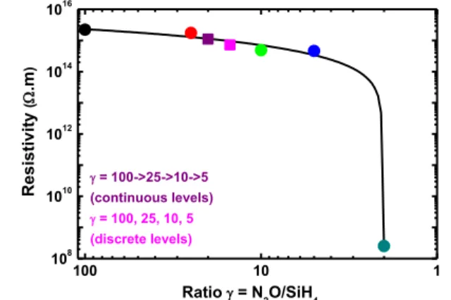
The joint effect of the properties of different mono-layers is confirmed also by the volume resistivity of the nanostructured layers. The resistivity of nanostructured layers with discrete and continuous levels is well aligned with the resistivity of mono-layers, having values averaged on the constituent levels (Fig. 7). The dielectric engineering permits modulation of the conductive dielectric properties of nanostructures over 7 orders of magnitude as can be seen in Fig. 7. The measured apparent dielectric permittivity of the nanostructured layers with discrete and continuous levels, represented in Fig. 7, is the same
grad5 = 4.35 [26], being quite higher than the one of silica layer.
Combined effect of increased dielectric constant with fast charge decay in the nanostructured layers qualifies them as appropriate for application in capacitive RF MEMS switches.
B. Silica layers with tailored interfaces
We show below that tailoring the properties of a SiO2 layer can be achieved by embedding a single layer of AgNPs (below the percolation threshold) in the vicinity of the free surface of a covering organosilicon and/or silica layer. When isolated, the AgNPs play the role of deep permanent trapping centers and collect charges injected within the dielectric cover layer. This strategy has been demonstrated in the case of nanocomposite layer of AgNPs embedded in organosilicon matrix (SiOxCy:H) covering a thick polyethylene material: mitigation of the charge injection can be achieved through trapping of charges on the AgNPs with virtually no more space charge build observed in the bulk of the polymer [33]. Control of charge injection phenomenon in that way certainly adds value to the operation and reliability of electronic devices containing dielectric layers, like in RF MEMS capacitive switches. Indeed, control of the fate of charges that will cross the potential barrier between the electrode and the highly insulating layer at the moment of injection by trapping on the AgNPs, appears possible. When properly dimensioned (size, shape, surface density and distance between the AgNPs), the AgNPs form hopping states in 2D along the AgNPs single layer. In this way, charges injected from protrusions of the membrane of the MEMS switch with electrostatic actuation will be laterally spread and released both during actuation and in the “off” state [12]. The design combines the high barrier to injection provided by the SiO2 layer with limitation of its charge trapping capabilities, thereby improving the global efficiency of the layer. Actually, appropriate materials go with optimization of the AgNPs size and density and the dielectric cover layer composition and thickness.
Bright field TEM images of a nanostructured layer, deposited according the above described concept, in cross-section and plane view are shown in Fig. 8. The determined characteristics of AgNPs from image processing are as follow: the AgNPs mean size is 19.6 ± 7.8 nm and their density equals 1.7 × 10¹¹ NPs/cm2, covering an area of 42.6%. For the high applied power to sustain the plasma (P = 80 W) the shape of the obtained AgNPs corresponds to a prolate spheroid. The single layer of AgNPs is not percolated. The characteristics of the AgNPs layer can be modulated by varying the plasma operation conditions.
TABLEI
SUMMARY OF THE PROCESSES FOR CHARGE RELEASE
IN DIFFERENT A-SIOXNY:H LAYERS Layer Thickness d (nm) FWHM (µm) of the charge spot Charge spot spreading after 500 s, in % Related mechanism = 100 116 0.91 2% No discharge = 25 193 0.68 1% No discharge = 10 207 20.47 180% Lateral = 5 175 4.67 40% Bulk+Lateral = 2 158 3.66 20% Bulk+Lateral grad5 173 7.62 150% Lateral+Bulk grad2 188 10.67 135% Lateral+Bulk
Fig. 7. Resistivity of mono-layers with different -values and of two nanostructured layers: = 100→25105 (continuous levels, purple square) and = 100, 25, 10, 5 (discrete levels, magenta square). The line is shown only as guide to the eye.
100 10 1 108 1010 1012 1014 1016 = 100->25->10->5 (continuous levels) = 100, 25, 10, 5 (discrete levels) Ratio = N 2O/SiH4 Re s isti v it y ( .m )
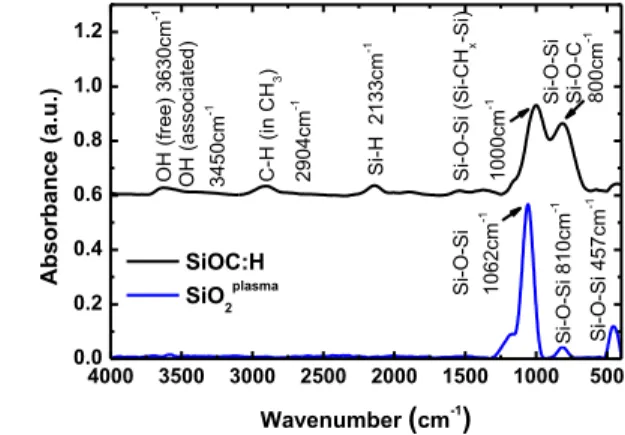
Two types of plasma deposits were electrically tested as cover layers: plasma silica (SiO2plasma) and organosilicon (SiOxCy:H) layers. As can be seen on the FTIR spectrum (Fig. 9) the plasma deposited SiO2plasma layer represents the features of thermal silica layer. One can observe the three typical transversally optic (TO) modes of molecular vibrations of amorphous silica [29, 34]: the Si-O-Si rocking vibration at 457 cm-1, the symmetric stretching mode at 810 cm-1, and the
asymmetric stretching mode at 1062 cm-1. The shoulder
centered around 1250 cm-1, characteristic of thermal SiO 2 is
clearly observable on the spectrum. The organosilicon layer is much less ordered presenting two broad massifs centered around 800 cm-1 and 1000 cm-1 [27, 28]. The large pick width approves the amorphous structure of this layer. Because of the high applied power (P = 80 W) for sustaining the plasma, the HMDSO is strongly dissociated. It leads to appearance of the asymmetric stretching band Si-H at 2133 cm-1 in the SiO
xCy:H
layer spectrum. This band is as much intensive as the typically observed C-H asymmetric stretching band in CH3 environment at 2904 cm-1.
KFM measurements of the potential profile induced by charge injection during 1 min at 25 V for different tailored thermal SiO2 layers are shown in Fig. 10. The thicknesses, as measured by spectroscopic ellipsometry and confirmed by the TEM observations (Fig. 8a), of the SiO2plasma and the SiOxCy:H layers covering the AgNPs are dc = 20 nm and 24 nm, respectively. A nanostructure without AgNPs was tested for comparison in both cases (with plasma silica and with organosilicon cover layer).
The potential profiles reveal strong lateral charge spreading for the nanostructure with AgNPs covered by SiOxCy:H layer compared to the same structure without AgNPs. It means that the injected charges are transported through the SiOxCy:H layer to attain the AgNPs and then laterally spread from nanoparticle to nanoparticle inducing a large surface potential profile. Not only the FWHM is larger for the nanostructure with AgNPs (FWHM = 3.34 µm and 0.83 µm for the nanostructures with AgNPs and without AgNPs, respectively) but also the integrated intensity of the potential profile (Is = 8.3 Vµm and 1.6 Vµm for the nanostructures with AgNPs and without AgNPs, respectively) revealing a larger density of injected charges.
The highly insulating properties of SiO2plasma cover layer do not allow charge transport over the 20 nm layer thickness. The injected charges are stored on the layer surface close to the injecting point without possibility to attain the AgNPs (FWHM = 0.72 µm). The integrated intensity of the measured potential profile is only of Is = 1.85 Vµm, a bit larger than the one obtained for the structure without AgNPs covered with SiOxCy:H layer and comparable to the values obtained for the highly insulating a-SiOxNy:H layers described in the previous section ( = 100 and 25 with Is = 2.0 Vµm and 1.4 Vµm, respectively) for the same injection conditions, 1 min at 25 V.
Fig. 8. Bright field TEM images of SiO2 layers with tailored interfaces:
(a) XS-TEM image and (b) PV-TEM image. SiO2plasma
AgNPs
SiO2
(a)
Fig. 9. FTIR spectra of the SiO2plasma and SiOxCy:H cover layers.
4000 3500 3000 2500 2000 1500 1000 500 0.0 0.2 0.4 0.6 0.8 1.0 1.2 80 0cm -1 S i-O -S i ( S i-C Hx -S i) 10 00 cm -1 S i-H 21 33 cm -1 C -H ( in C H3 ) 29 04 cm -1 SiOC:H SiO2plasma Ab so rb an ce ( a.u.) Wavenumber (cm-1) Si -O -Si 1 0 6 2 cm -1 S i-O-Si 8 1 0 cm -1 Si -O -Si 4 5 7 cm -1 O H ( fr ee ) 36 30 cm -1 O H ( asso ci ated) 34 50 cm -1 S i-O -S i S i-O -C
Fig. 10. KFM measurements of the potential profiles induced by charge injection during 1 min at 25 V for tailored SiO2 layers.
-10 -5 0 5 10 0.0 0.5 1.0 1.5 2.0 2.5 3.0 SiOC:H/AgNPs/SiO2 SiO2pl /AgNPs/SiO2 SiOC:H/SiO2 Position (µm) P o te n tia l (V )
Fig. 11. Evolution with time of the integrated intensity (normalized to its value at 30 s) after injection for tailored SiO2 layers. Charge injection is performed for 1 min at 25 V.
0 200 400 600 800 0.0 0.2 0.4 0.6 0.8 1.0 1.2 SiOC:H(d=24nm)/AgNPs/SiO2 SiOC:H(d=24nm)/SiO2 SiO2pl(d=20nm)/AgNPs/SiO 2 Is /Is (t = 3 0 s )
The charge decay for the tailored with AgNPs silica layers is presented in Fig. 11. It is additionally accelerated by the presence of AgNPs when the cover layer is of SiOxCy:H of thickness of 24 nm. For only organosilicon layer, without AgNPs, the charges are trapped in the dielectric layer close to the injection point and no discharge is detected. The same behaviour is observed for the nanostructure containing AgNPs covered with SiO2plasma with thickness of 24 nm. For values of the applied bias of 25 V, the corresponding electric field on the AFM tip is in the order of 30-150 kV/mm, as calculated from electrostatic modeling [35]. It suggests that the layer thickness must be reduced to less than 5 nm to allow for tunneling.
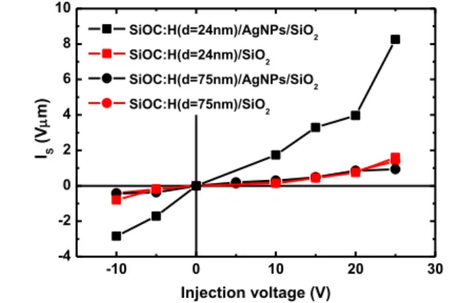
Results obtained for other applied injection voltages show that the integrated potential profile is always much larger for the nanostructure with embedded AgNPs in SiOxCy:H matrix at dc = 24 nm from the surface compared to a nanostructure without AgNPs (Fig. 12). This implies charging of the AgNPs. Moreover, it is true for both voltage polarities. However, when the AgNPs are embedded at a distance of 75 nm or larger from the free surface of SiOxCy:H cover layer their control on the dielectric charging phenomenon is substantially attenuated. It means that the conception of performant nanostructured layers requires fine control over many parameters of the two constituents of the layer: (i) properties of the AgNPs (mean size, density, morphology) and (ii) properties of the cover layer (composition, thickness, conductivity).
C. Potential applications of the presented nanostructured layers beyond the RF MEMS capacitive switches
The proposed approach in this contribution opens the way for transition from material level of development to system level of applications. The achieved fine control of structural and electrical properties of the presented nanostructured thin dielectrics approves the developed strategy of dielectric engineering of thin layers. As shown earlier, the dielectric engineering permits modulation of the conductive properties of nanostructures over several decades. Potential applications of these layers, beyond the MEMS/NEMS systems, can be found in quite different domains. The silicon oxynitride layers (a-SiOxNy:H) with gradual variation of their properties
(discrete or continuous) can successfully be used to better fit silicon based devices such as light emitters, optical modulators, single electron devices, non-volatile memory devices, as well as more recent developments in the field of “all-Si” tandem solar cells for third generation photovoltaics [4, 5, 36-38].
The multifunctionality of the second kind of presented
nanostructured dielectrics is quite large determining a great panel of applications. By combining the optical and electrical properties of the AgNPs with those of the host matrix (organosilicon or plasma silica), these layers can be considered for application in advanced solar cells by combining the plasmonic and charge trapping effects [39]. Since the AgNPs are known to realize the best nanoscale antenna for amplifying local electronic and vibrational signals in the visible range, these nanostructures can successfully be used as plasmonic substrates for spectroscopies based on surface-enhanced Raman scattering, having potential applications as ultra-sensitive sensors for chemical and biomolecular detection and analysis, photonic switches, etc. Moreover, the plasma process offers the possibility to overcome the limit imposed by their fabrication, replying in this way to the drastic requirements for controlling on a large area, and in a reproducible way, a well-defined spacing between the metallic nanoparticles and the probing molecules deposited on the surface of the plasmonic substrates [29]. A strongly original application of the nanostructured dielectrics containing AgNPs is related to their use in microbiology to modulate the activity of silver nanostructured surfaces by tuning the release of Ag+ and/or AgNPs, thus the toxicity of
nanocomposite materials to the exposed media [40].
For many industrial purposes, like for high voltage DC (HVDC) applications (e.g. HVDC cables with polymeric insulation), the phenomenon of charge injection in dielectric layers under electrical stress is at the origin of space charge formation. The space charge must be avoided because it gives contribution to the electric field distribution inducing a departure from the designed one and represents a risk for breakdown, especially under voltage reversal. To bring a solution to this problem one can tailor the surface of the polymer with the nanostructured layers containing a single layer of AgNPs in order to insert a thin layer of material with adequate properties in between the electrode and the polymer to counteract the injection process to the material defects or traps. The AgNPs represent artificial trapping centers for the injected charges, thereby reducing the electric field at the contact. Efficient charge trapping for both polarities due to the ability of AgNPs to store positive or negative charges was recently reported [33, 41]. The host matrix guarantees the transport of injected charges to the AgNPs permanent traps. Given the performance of the nanostructured layers for applied electric fields well above the typical service fields for HVDC applications, a potential application of these layers can also be explored in the domain of power electronics.
CONCLUSION
Dielectric engineering of thin dielectrics is applied to develop a new class of nanostructured dielectric layers controlling the charge transport in thin dielectric layers:
Fig. 12. Integrated potential profiles after 1 min of charge injection as a function of the injection voltage for two thicknesses of the SiOxCy:H cover
layer in presence of AgNP and without AgNPs.
-10 0 10 20 30 -4 -2 0 2 4 6 8 10 SiOC:H(d=24nm)/AgNPs/SiO2 SiOC:H(d=24nm)/SiO2 SiOC:H(d=75nm)/AgNPs/SiO2 SiOC:H(d=75nm)/SiO2 IS ( V m ) Injection voltage (V)
(i) silicon oxynitride layers with gradual properties, and (ii) silica layers with tailored interfaces. Both are achieved by plasma deposition processes. The obtained results show that strong gradual variation of the conductive properties across the nanostructured dielectrics provides efficient charge transport in depth of the structure and reduces the electric field at the surface, decreasing in that way the density of injected charges. In the second kind of presented structures a single layer of AgNPs embedded in the vicinity of an organosilicon (SiOxCy:H) free surface (up to about 25 nm in depth) efficiently blocks the electrical charge injection in thin dielectric layers. When tailoring with SiO2plasma cover layer, the thickness of the cover layer should be reduced to the one allowing tunneling in order to charge the AgNPs. Synthesizing nanocomposite layers with high AgNPs density allows capturing the injected charges that crosses the plasma
SiO2plasma layer and force their lateral spreading so as to locally
reduce electrostatic forces. Both nanostructured layers presented in this study appear quite promising for application in RF MEMS capacitive switches with electrostatic actuation.
REFERENCES
[1] C. Laurent, G. Teyssedre, S. Le Roy, and F. Baudoin, “Charge dynamics and its energetic features in polymeric materials,” IEEE Trans. Dielectr.
Electr. Insul., vol. 20, pp. 357–381, 2013.
[2] M. Taleb, G. Teyssèdre, S. Le Roy, and C. Laurent, “Modeling of charge injection and extraction in a metal/polymer interface through an exponential distribution of surface states,” IEEE Trans. Dielectr. Electr.
Insul., vol. 20, pp. 311–320, 2013.
[3] T. Tanaka, “Dielectric nanocomposites with insulating properties,” IEEE
Trans. Dielectr. Electr. Insul., vol. 12, pp. 914–928, 2005.
[4] P. Normand, E. Kapetanakis, P. Dimitrakis, D. Skarlatos, D. Tsoukalas, K. Beltsios, A. Claverie, G. Benassayag, C. Bonafos, M. Carrada, N. Cherkashin, V. Soncini, A. Agarwal, Ch. Sohl, and M. Ameen, “Effects of annealing conditions on charge storage of Si nanocrystal memory devices obtained by low-energy ion beam synthesis,” Microelectron.
Eng., vol. 67–68, pp. 629–634, 2003.
[5] S. Perret-Tran-Van, K. Makasheva, B. Despax, C. Bonafos, P. E. Coulon, and V. Paillard, “Controlled fabrication of Si-nanocrystals embedded in thin SiON layers by PPECVD followed by oxidizing annealing,” Nanotechnology, vol. 21, p. 285605, 2010.
[6] G. M. Sessler, “New applications of electrets,” Proceedings of the 8th
International Symposium on Electrets (ISE 8), pp. 937–942, 1994.
[7] G. M. Rebeiz, RF MEMS Theory, Design, and Technology, Hoboken, New Jersy: John Wiley & Sons, Inc., 2003.
[8] See http://www.esda.org for more information about ElectroStatic Discharge (ESD) influence on electronic devices.
[9] W. M. Zhang, G. Meng, and D. Chen, “Stability, nonlinearity and reliability of electrostatically actuated MEMS devices,” Sensors, vol. 7, pp. 760–796, 2007.
[10] G. Papaioannou, M. Exarchos, V. Theonas, G. Wang, J. Papapolymerou, "Temperature study of the dielectric polarization effects of capacitive RF MEMS switches," IEEE Trans. Microw. Theory Tech., vol. 53, pp. 3467–3473, 2005.
[11] U. Zaghloul, B. Bushan, P. Pons, G. J. Papaioannou, F. Coccetti, and R. Plana, “A systematic reliability investigation of the dielectric charging process in electrostatically actuated MEMS based on Kelvin force microscopy,” J. Micromech. Microeng., vol. 20, p. 064016, 2010. [12] C. Villeneuve, P. Pons, V. Puyal, and R. Plana, "Planarization
optimization of RF MEMS switches with a gold membrane", J.
Micromech. Microeng, vol. 20, p. 064013, 2010.
[13] U. Zaghloul, B. Bushan, P. Pons, G. J. Papaioannou, F. Coccetti, and R. Plana, “On the influence of environment gases, relative humidity and gas purification on dielectric charging/discharging processes in electrostatically driven MEMS/NEMS devices,” Nanotechnology, vol. 22, p. 035705, 2011.
[14] G. Papaioannou, “The Impact of Dielectric Material and Temperature on Dielectric Charging in RF MEMS Capacitive Switches,” in Advanced
Materials and Technologies for Micro/Nano-Devices, Sensors and Actuators, Springer Ed.: Netherlands, pp. 141–153, 2010.
[15] N. Tavassolian, M. Koutsoureli, E. Papandreou, G. Papaioannou, B. Lacroix, Z. Liu, J. Papapolymerou, “The Effect of Silicon Nitride Stoichiometry on Charging Mechanisms in RF MEMS Capacitive Switches,” IEEE Transactions on Microwave Theory and Techniques, vol. 57, pp. 3518-3524, 2009.
[16] All quoted dielectric constants apply for 1 kHz and 23°C.
[17] S. Bécu, S. Crémer, and J. L. Autran, “Capacitance non-linearity study in Al2O3 MIM capacitors using an ionic polarization model,”
Microelectronic Engineering, vol. 83, pp. 2422-2426, 2006.
[18] J. Robertson, “High dielectric constant oxides,” Eur. Phys. J. Appl.
Phys., vol. 28, pp. 265–291, 2004.
[19] C. Bordas, K. Grenier, D. Dubuc, E. Flahaut, S. Pacchini, M. Paillard, and J.-L. Cazaux, “Carbon nanotube based dielectric for enhanced RF MEMS reliability,” IEEE/MTT-S International Microwave Symposium, pp. 375–378, 2007.
[20] L. Michalas, S. Xavier, M. Koutsoureli, O. El Jouaidis, S. Bansropun, G. Papaioannou, and A. Ziaei, "Gold nanorod array structured silicon nitride films for reliable RF MEMS capacitive switches," IEEE 15th
Topical Meeting on Silicon Monolithic Integrated Circuits in RF Systems (SiRF), pp. 89–91, 2015.
[21] L. Michalas, M. Koutsoureli, S. Saada, C. Mer–Calfati, A. Leuliet, P. Martins, S. Bansropun, G. Papaioannou, P. Bergonzo, and A Ziaei, “Electrical assessment of diamond MIM capacitors and modeling of MEMS capacitive switch discharging,” Journal of Micromech.
Microeng., vol. 24, p. 115017, 2014.
[22] O. Auciello, J. Birrell, J. A. Carlisle, J. E. Gerbi, X. Xiao, B. Peng, and H. D. Espinosa, “Materials science and fabrication processes for a new MEMS technology based on ultrananocrystalline diamond thin films,” J.
Phys.: Condens. Matter, vol. 16, pp. R539–R552, 2004.
[23] S. Bhattacharyya, O. Auciello, J. Birrell, J. A. Carlisle, L. A. Curtiss, A. N. Goyette, D. M. Gruen, A. R. Krauss, J. Schlueter, A. Sumant, and P. Zapol, “Synthesis and characterization of highly-conducting nitrogen-doped ultrananocrystalline diamond films,” Appl. Phys. Lett., vol. 79, pp. 1441–1443, 2001.
[24] C. Goldsmith, A. Sumant, O. Auciello, J. Carlisle, H. Zeng, J. C. M. Hwang, C. Palego, W. Wang, R. Carpick, V. P. Adiga, A. Datta, C. Gudeman, S. O'Brien, and S. Sampath, “Charging characteristics of ultra-nano-crystalline diamond in RF MEMS capacitive switches,” IEEE
MTT-S International Microwave Symposium Digest (MTT), pp. 1246–
1249, 2010.
[25] X. Zang, Q. Zhou, J. Chang, Y. Liu, and L. Lin, “Graphene and carbon nanotube (CNT) in MEMS/NEMS applications,” Microelectronic
Engineering, vol. 132, pp. 192–206, 2015.
[26] K. Makasheva, B. Despax, L. Boudou, and G. Teyssedre, “Dielectric layers for RF-MEMS switches: design and study of appropriate structures preventing electrostatic charging,” IEEE Trans. Dielectr.
Electr. Insul., vol. 19, pp. 1195–1202, 2012.
[27] B. Despax and P. Raynaud, “Deposition of “Polysiloxane” Thin Films Containing Silver Particles by an RF Asymmetrical Discharge”, Plasma
Process. Polym., vol. 4, pp. 127–134, 2007.
[28] K. Makasheva, C. Villeneuve-Faure, S. Le Roy, B. Despax, L. Boudou, C. Laurent, and G. Teyssedre, “Silver nanoparticles embedded in dielectric matrix: charge transport analysis with application to control of space charge formation,” Annual Report IEEE Conference on Electrical
Insulation and Dielectric Phenomena -CEIDP-, vol. 1, pp. 238–241,
2013, DOI: 10.1109/CEIDP.2013.6747079
[29] A. Pugliara, C. Bonafos, R. Carles, B. Despax,and K. Makasheva, “Controlled elaboration of large-area plasmonic substrates by plasma process,” Material Research Express, vol. 2, p. 065005, 2015.
[30] C. Villeneuve-Faure, K. Makasheva, C. Bonafos, B. Despax, L. Boudou, P. Pons, and G. Teyssedre, “Kelvin force microscopy characterization of charging effect in thin a-SiOxNy:H layers deposited in pulsed plasma enhanced chemical vapor deposition process by tuning the silicon environment,” J. Appl. Phys., vol. 113, p. 204102, 2013.
[31] S. Schamm, C. Bonafos, H. Coffin, N. Cherkashin, M. Carrada, and G. Ben Assayag, “Imaging Si nanoparticles embedded in SiO2 layers by (S)TEMEELS,” Ultramicroscopy, vol. 108, pp. 346–357, 2008. [32] N. Knorr, S. Rosselli, and G. Nelles, "Surface-potential decay of
biased-probe contact-charged amorphous polymer films," J. Appl. Phys., vol. 107, p. 054106, 2010.
[33] L. Milliere, K. Makasheva, C. Laurent, B. Despax, and G. Teyssedre, "Efficient barrier for charge injection in polyethylene by silver
nanoparticles/plasma polymer stack," Appl. Phys. Lett., vol. 105, p. 122908, 2014.
[34] C. T. Kirk, “Quantitative analysis of the effect of disorder-induced mode coupling on infrared absorption in silica,” Phys. Rev. B, vol. 38, pp. 1255-1273, 1988.
[35] A. Boularas, F. Baudouin, C. Villeneuve-Faure, S. Clain and G. Teyssedre “Multi-dimensional modelling of electrostatic force distance curve over dielectric surface: Influence of tip geometry and correlation with experiment,” J. Appl. Phys., vol. 116, p. 084106, 2014.
[36] R. Rao, R. Steimle, M. Sadd, C. Swift, B. Hradsky, S. Straub, T. Merchant, M. Stoker, S. G. Anderson, M. Rossow, J. Yater, B. Acred, K. Harber, E. Prinz, B. White, and R. Muralidhar, “Silicon nanocrystal based memory devices for NVM and DRAM applications,” Solid-State
Electronics, vol. 48, pp. 1463–1473, 2004.
[37] G. Conibeer, M. Green, E. Cho, D. Konig, Y. Cho, T. Fangsuwannarak, G. Scardera, E. Pink, Y. Huang, T. Puzzer S. Huang, D. Song, C. Flynn, S. Park, X. Hao, and D. Mansfield, “Silicon quantum dot nanostructures
for tandem photovoltaic cells,” Thin Solid Films, vol. 516, pp. 6748– 6756, 2008.
[38] J. Barbé, K. Makasheva, S. Perraud, M. Carrada, and B. Despax, “Structural analysis of the interface of silicon nanocrystals embedded in Si3N4 matrix,” J. Phys. D: Appl. Phys., vol. 47, p. 255302, 2014.
[39] H. Choi, W. T. Chen, and P. V. Kamat, “Know Thy Nano Neighbor. Plasmonic versus Electron Charging Effects of Metal Nanoparticles in Dye-Sensitized Solar Cells,” ACS NANO, vol. 6, pp. 4418-4427, 2012. [40] A. Pugliara, K. Makasheva, B. Despax, M. Bayle, R. Carles, P. Benzo,
G. BenAssayag, B. Pécassou, M.-C. Sancho, E. Navarro, Y. Echegoyen, and C. Bonafos, “Assessing bio-available silver released from silver nanoparticles embedded in silica layers using the green algae
Chlamydomonas reinhardtii as bio-sensors,” Sci. Total Environ., 2016,
in press, http://dx.doi.org/10.1016/j.scitotenv.2016.02.141
[41] L. Milliere, K. Makasheva, C. Laurent, B. Despax, L. Boudou, and G. Teyssedre, “Silver nanoparticles as a key feature of a plasma polymer composite layer in mitigation of charge injection into polyethylene under dc stress,” J. Phys. D: Appl. Phys., vol. 49, p. 015304, 2016.