Ab initio study of electron transport in lead
telluride
by
Qichen Song
Submitted to the Department of Mechanical Engineering
in partial fulfillment of the requirements for the degree of
Master of Science in Mechanical Engineering
at the
MASSACHUSETTS INSTITUTE OF TECHNOLOGY
February 2018
c
○ Massachusetts Institute of Technology 2018. All rights reserved.
Author . . . .
Department of Mechanical Engineering
Jan 16, 2018
Certified by . . . .
Gang Chen
Carl Richard Soderberg Professor of Power Engineering
Thesis Supervisor
Accepted by . . . .
Rohan Abeyaratne
Chairman, Department Committee on Graduate Students
Ab initio
study of electron transport in lead telluride
by
Qichen Song
Submitted to the Department of Mechanical Engineering on Jan 16, 2018, in partial fulfillment of the
requirements for the degree of
Master of Science in Mechanical Engineering
Abstract
Last few years have witnessed significant enhancement of thermoelectric figure of merit of lead telluride (PbTe) via nanostructures. Despite the experimental progress, current understanding of the electron transport in PbTe is based on either band structure simulated using first-principles in combination with constant relaxation time approximation or empirical models, both requiring adjustable parameters obtained by fitting experimental data.
This thesis aims to compute thermoelectric properties of PbTe all from first-principles. We start by discussing the formalism based on Boltzmann transport equa-tion to calculate the electron transport properties in PbTe using first principles and identify the importance to calculate electron-phonon interaction accurately. We then discuss the challenges in studying electron-phonon interaction in semiconductors us-ing first-principles and introduce electron-phonon Wannier interpolation which allows us to calculate the strength of electron-phonon coupling on a very fine mesh. In polar materials like PbTe, the Fröhlich interaction due to long-range dipole field of longi-tudinal optical phonons contributes to the electron-phonon coupling as well. As the long-range nature of the dipole field makes the standard Wannier interpolation fail, we have discussed the detailed procedures for correction. Next, we study the screen-ing effect of free carriers on electron transport by modulatscreen-ing the polar scatterscreen-ing. These considerations enabled us to report parameter-free first-principles calculation of electron and phonon transport in PbTe, including mode-by-mode electron-phonon scattering, leading to detailed information on electron mean free paths and the cu-mulative contributions by electrons and phonons with different mean free paths to thermoelectric transport properties in PbTe. Such information will help to rationalize the use and optimization of nanosctructures to achieve high thermoelectric figure of merit.
Thesis Supervisor: Gang Chen
Acknowledgments
I would like to thank my advisor, Professor Gang Chen for providing the guidance and source for my research. He initiates the direction of this project and allows me to conduct research in my own way. His critical thinking on this research topic not only helps me identify critical issues but inspires me to become a thorough researcher.
I want to thank Professor David Broido at Boston College, Professor Gerald Denise Mahan, Professor Zhifeng Ren at University of Houston, Professor Boris Kozinsky at Harvard, Professor Qian Zhang at Harbin Institute of Technology, Professor Bolin Liao at UCSB, and Professor Mingda Li at MIT for the insightful discussions.
Also, I am thankful for my lab mates, Doctor Te-Huan Liu, Jiawei Zhou, Yoichiro Tsurimaki, Samuel Huberman, Doctor Jonathan Mendoza and Qian Xu for the useful discussions. I want to thank Ms. Keke Xu and Ms. Juliette A. Pickering for the assistance in the laboratory.
I am very thankful for the funding support from DOE S3TEC. The center provides fantastic collaborative working and DARPA MATRIX program for supporting the computational code development.
I am grateful for my friends Haozhe Wang, Dr. Meng An for the encouraging my pursuit of this work. In particular, I would like to express my appreciation for the generous support of my life from my girlfriend, Mengying Wu.
Last but not least, I want to thank my family. When pursuing this degree, I have not been able to come back home for more than two years while my parents show great patience and endless love to me. Such unconditional love means so much to me.
Contents
1 Introduction 15
1.1 Motivations for nanostructuring the thermoelectric materials . . . 16
1.2 Electron transport properties of interest in thermoelectric materials . 18 1.2.1 Linearized Boltzmann transport equation for electrons . . . . 19
1.2.2 Electron transport properties and electron mean free paths . . 20
1.3 Electron scattering rate . . . 25
1.4 A brief review of previous computational work . . . 28
1.5 Outline of the thesis . . . 30
2 Lattice dynamics from first principles 31 2.1 Density functional theory . . . 31
2.1.1 Hartree approximation . . . 32
2.1.2 Hartree-Fock approximation . . . 33
2.1.3 Kohn-Sham equation, local density approximation and pseu-dopotentials . . . 34
2.2 Density functional perturbation theory . . . 36
2.2.1 Linear response theory . . . 37
2.2.2 General form of perturbed potential . . . 38
2.3 Phonons in polar materials . . . 38
2.3.1 Nonanalytical force constant in polar materials . . . 39
2.3.2 The screening effect of free carriers on phonons . . . 40 2.3.3 Phonon dispersion of PbTe with different carrier concentrations 42
3 Electron-phonon interaction in from first principles 45
3.1 Electron-phonon interaction to the lowest order . . . 46
3.2 Electron-phonon Wannier interpolation . . . 47
3.2.1 Maximumly localized Wannier function . . . 47
3.2.2 Electron-phonon coupling matrix in the Wannier representation 49 3.3 Electron-phonon coupling matrix in polar materials . . . 50
3.3.1 Screened Fröhlich interaction . . . 50
3.3.2 Electron-phonon coupling matrix for different phonon polariza-tion in PbTe . . . 52
3.4 Relaxation time approximation . . . 55
3.4.1 Electron-phonon scattering rate . . . 55
3.4.2 Phonon scattering rate by electrons . . . 57
4 The electron mean free paths and transport properties in PbTe 61 4.1 Ab initio thermoelectric transport properties . . . 62
4.1.1 The effect of screening . . . 62
4.1.2 The effect of temperature . . . 64
4.2 Weakly isotropic scattering rates in PbTe . . . 69
5 Summary and future work 73 5.1 Summary . . . 73
5.2 Future work . . . 74
5.2.1 Symmetry analysis on the electron-phonon coupling matrix . . 74
5.2.2 Scattering by the grain boundary . . . 75
A Lindhard dielectric function 77
B Anisotropic effective mass of electrons 85
List of Figures
1-1 The origin of the long-range dipole field due to LO phonon in polar material consisting two atoms per unit cell. . . 28 2-1 The screening effect of free carriers on the optical phonon modes. At
the limit of 𝑞 → 0, the LO and TO modes converges given strong enough screening effect . . . 41 2-2 The inverse of the Thomas-Fermi wavevector (1/𝑘𝑇 𝐹) — screening
ra-dius as a function of carrier density from DFT and from parabolic band model. . . 42 2-3 The phonon dispersion for different free carrier concentrations
com-pared with neutron scattering experiment[10]. . . 44 3-1 The maximumly localized Wannier orbitals of Pb and Te in PbTe
with-out spin-orbit coupling. The symmetry of the material is not conserved during the iterative process of minimizing the localization functional. 49 3-2 The amplitude of the electron-phonon coupling matrix element for
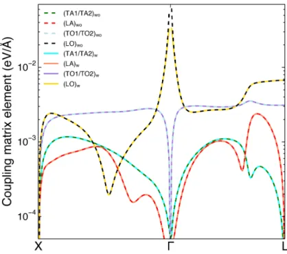
elec-tron at conduction band minimum and phonons at the high-symmetry paths with/without considering screening in the long-range (Fröhlich) part of the electron-phonon coupling matrix. The carrier concentration is 1018cm−3. . . . 53
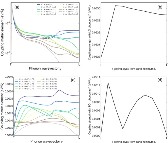
3-3 The amplitude of the electron-phonon coupling matrix element includ-ing screeninclud-ing effect for electrons at L → Γ path and LO/TO phonons at Γ → L. In (a) and (c), different colors mark different electron states. In (b) and (d), the strength of the coupling between Γ point LO/TO phonon and different electron states are shown. Note that for LO phonon, the exact 𝑞 = 0 behavior cannot be calculated due to the divergence shown in Eq. 3.14 thus we use 𝑞 = 0.01×𝑙ΓL= 0.01×
√ 3 2
𝜋 𝑎 to
represent the extreme case 𝑞 = 0. The carrier concentration is 1018cm−3. 54
3-4 (a-b) The energy-resolved electron-phonon scattering rates for conduc-tion band electrons due to phonon modes of different branches at 300 K with/without considering the screening effect. The zero energy marks the conduction band minimum and the dashed line indicates the loca-tion of chemical potential. The carrier concentraloca-tion is 2.3 ×1019cm−3. 56 3-5 The scattering rate for phonons due to electron-phonon interaction
compared with the scattering rate due to phonon-phonon interaction at 300 K with the carrier concentration of 1021cm−3. . . . . 58
4-1 (a) The mobility, (b) the electrical conductivity, (c) the Seebeck co-efficient, and (d) the power factor of PbTe as a function of carrier concentration at 300 K with and without considering the screening effect. Dotted lines are from simulation and isolated dots are experi-mental value. The triangles are from Ref.[26], squares from Ref.[54], diamonds from Ref.[67], and crosses from Ref.[15]. . . 63
4-2 (a) The electron mean free path as a function of energy with and with-out considering the screening effect. The dashed line indicates the chemical potential and zero energy indicates the conduction band min-imum. (b) The accumulated electrical conductivity with respect to electron mean free path. (c) The normalized truncated Seebeck coeffi-cient with respect to the electron mean free path. (d) The normalized truncated power factor with respect to electron mean free path com-pared with normalized accumulated phonon thermal conductivity with respect to phonon mean free path. The dopant concentration is 2.3 ×1019cm−3. . . . 65
4-3 The electron mean free path as a function of energy at different tem-peratures. The dashed line indicates the chemical potential and zero energy corresponds the conduction band minimum. The dopant con-centration is 5.8 ×1019cm−3. . . . . 66
4-4 (a) The accumulated electrical conductivity with respect to electron mean free path. The normalized truncated (b) Seebeck coefficient and (c) power factor with respect to electron mean free path. (d) The accumulated lattice thermal conductivity with respect to phonon mean free path. The dopant concentration is 5.8 ×1019cm−3. . . 67 4-5 (a) The conductivity, (b) the Seebeck coefficient, (c) the electronic
thermal conductivity compared with phonon thermal conductivity, (d) the bipolar thermal conductivity, (e) the total thermal conductivity and (f) the figure of merit 𝑧𝑇 of PbTe as a function of temperature for different ionized donor concentrations. The squares are experimental results from Ref.[54] . . . 69 4-6 Electron-phonon scattering rates for different phonon polarizations mapped
into the electron band structure. L → W is light-mass direction and L → Γ is the heavy mass-direction. . . 71
List of Tables
B.1 The longitudinal and transverse effective mass of PbTe from calculation and experiment[31] . . . 86 B.2 The DOS and conductivity effective mass of PbTe from calculation and
Chapter 1
Introduction
Heat and electricity are two forms of energy both playing essential roles in our life. Electricity is the phenomena regarding the flow of charge. It is controllable, versatile and energizes all kinds of equipment. Heat, on the other side, is the process regarding the flow of thermal energy. It originates from the stochastic motion of atoms mea-sured by temperature thus can be found everywhere. The demand for electricity stim-ulates several thermal-to-electrical energy conversion technologies, such as thermion-ics, thermoelectrthermion-ics, and thermophotovoltaics. The thermionics/thermophotovoltaics involve spontaneous emission of electrons/photons such that they both require a high-temperature heat source. In contrast, thermoelectric devices can work at various temperature ranges. As a result, thermoelectric devices are considered as potential candidates to convert waste heat into useful electricity. To realize such applications, a comprehensive understanding of the physical process happening inside the thermo-electric devices is crucial. In solid-state thermothermo-electric materials, thermo-electricity is carried by either electrons or holes while heat is carried by energy carriers including elec-trons, holes, phonons, magnons. The essences of thermoelectric effects are transport phenomena of those carriers. The study of the transport process is indeed a study of the interplay of the charge and heat carriers.
A typical thermoelectric device composes of an n-doped and a p-doped semicon-ductor “leg” combined between the heat source and sink. The carriers in each leg are driven out of equilibrium by the temperature gradient to form a flow. In n-doped
semiconductors, electrons are thermally excited at the hot side and diffuse towards the cooler side. An electrical potential difference is generated correspondingly. Such phenomenon is named as Seebeck effect and the Seebeck coefficient is 𝑆 = −∆𝑉 /∆𝑇 . Meanwhile, phonons are migrating from the heat source towards sink. During the nonequilibrium transport process, the electrons/holes are charge and heat carriers, and phonons are heat carriers. From a thermodynamics point of view, to maximize the efficiency of thermoelectric power generator, we want the work — electrical power to be maximized, and less heat dumped into the heat sink. In other words, higher electrical conductivity, larger Seebeck coefficient and lower thermal conductivity at the same time are desired.
1.1
Motivations for nanostructuring the
thermoelec-tric materials
In 1993, L. D. Hicks and M. S. Dresselhaus pointed out in two pioneering papers[28][29] that a quantum-well structure and one-dimensional conductor can significantly in-crease the figure of merit 𝑧𝑇 , a dimensionless quantity that measures the thermo-electric performance of the material. Essentially, in low-dimension thermothermo-electric materials, the density of states near the conduction/valence band edge are much higher than their three-dimensional bulk correspondent[13]. These findings inspired people to think of controlling materials at nanoscale and brought profound changes to the thermoelectric community. From the 1940s to 1990s, the maximum 𝑧𝑇 was only slowly increasing over time from about 0.1 to about 1. After 1993 when the idea of nanostructuring was proposed, the 𝑧𝑇 value has been increasing with time, eventually above 2.5[27]. Past works have also successfully increased the thermoelectric efficiency by reducing the phonon thermal conductivity. In silicon, for example, the electron mean free paths from first-principles calculation are around tens of nanometers[58], while phonons have mean free paths up to a few microns[14]. As a result, nanos-tructures with grain sizes between the electron and phonon mean free path strongly
scatter phonons and reduce thermal conductivity dramatically yet have minimal ef-fects on the electrical transport[58]. Such kind of enhancement of thermoelectric performance has also been observed in the experiment for nanocrystalline silicon[52]. Compared with low-dimensional nanostructures, the bulk nanostructuring approach might be applied in more general conditions[33].
The first-principles calculation scheme much facilitated the understanding of phonon transport and the phonon thermal conductivity in nanostructures. In such scheme, the lattice dynamics is obtained by either supercell approach (real space) or density functional perturbation approach (reciprocal space). By solving the linearized phonon Boltzmann transport equation either iteratively[37] or adopting relaxation time ap-proximation, the behavior of each phonon mode can be resolved. The ab initio calcu-lation of intrinsic phonon transport shows excellent agreement with experiment[71]. With the detailed information of phonon such as phonon mean free paths, experimen-talists know what the expected grain size is that the phonon are much more efficiently scattered. However, this is only one side of the story. To avoid any deterioration of electron transport due to the nanostructures, the information on electron dynamics is needed. Surprisingly, a fully first-principles calculation for electron transport with a similar level of details for phonons is rarely reported. This motives us to find an accurate approach to calculate the electron transport properties with mode-by-mode resolution.
Several groups reported high figure of merit in PbTe through different nanostruc-turing approaches [78][6][55][56][77]. One beneficial feature of PbTe is its low intrinsic thermal conductivity due to the strong anharmonicity[12][35][70]. For PbTe, the ther-mal transport has also been examined from the first principles yielding that phonons with mean free paths smaller than 10 nm contribute the majority of the thermal conductivity. This implies that to reduce the thermal conductivity, the grain sizes should be in the order of magnitude of 10 nm. Biswas et al. proposed a “panoscopic” approach that mesoscale grain boundaries (100 — 103 nm) can scatter phonons with
different mean free paths. As a result, they claim that the maximum reduction of the thermal conductivity is achieved. Meanwhile, the electrical transport properties
are not compromised. Particularly, the Seebeck coefficient slightly increases. A phe-nomenological model by Martin has attribute it to interface barrier scattering[46]: the interface barrier that impedes low-energy electron conduction between grains leads to enhanced Seebeck coefficient. Due to the lack of intrinsic electron mean free path calculation, such model is yet to be justified. To understand the origin of the out-standing performance of nanostructured PbTe, we believe it is necessary to carry out the first-principles calculation of electron transport properties.
1.2
Electron transport properties of interest in
ther-moelectric materials
The maximum efficiency of a thermoelectric device is defined by,
𝜂max = 𝑇𝐻 − 𝑇𝐶 𝑇𝐶 √ 1 + 𝑍 ¯𝑇 − 1 √ 1 + 𝑍 ¯𝑇 + 𝑇𝐶 𝑇𝐻 , (1.1)
where 𝑇𝐻 and 𝑇𝐶 are the absolute temperatures of hot side and cold side, and ¯𝑇
is the average temperature defined by (𝑇𝐻 + 𝑇𝐶)/2. The larger the temperature
difference between the hot side and cold side and the higher the average figure of merit 𝑍 ¯𝑇 , the higher the efficiency of the thermoelectric devices is. The figure of merit at temperature 𝑇 is only related to material properties as,
𝑧𝑇 = 𝜎𝑆
2𝑇
𝜅 (1.2)
where 𝜎 is the electrical conductivity, 𝑆 is the Seebeck coefficient, 𝜅 is the thermal conductivity consisting the contribution from electrons (𝜅𝑒), ambipolar diffusion (𝜅𝑏𝑝)
and phonons (𝜅𝑝ℎ), and 𝑇 is the temperature. In the following, the microscopic
1.2.1
Linearized Boltzmann transport equation for electrons
We start the derivation by writing down the Boltzmann transport equation for elec-trons, 𝜕𝑓𝑛k 𝜕𝑡 + v𝑛k · ∇r𝑓𝑛k+ F𝑛k · ∇p𝑓𝑛k = d𝑓𝑛k d𝑡 ⃒ ⃒ ⃒ ⃒ coll , (1.3)
where 𝑓𝑛k is the distribution function of the electron with band index 𝑛 and
momen-tum 𝑘. The force acted by electric field is F𝑛k = 𝑞E where 𝑞 = −𝑒 for electrons and
𝑞 = +𝑒 for holes. To simplify Eq 1.3, we make following approximations:
∙ The applied electrical field and temperature gradient are weak enough that the distribution function is slightly deviated from equilibrium. Also, the character-istic time scale of the variation of the distribution function is slow, such that the term 𝜕𝑓𝑛k/𝜕𝑡 ≈ 0.
∙ The existence of the external electrical field and temperature gradient only lead to small deviation of the distribution function from its equilibrium state. Electron is Fermion obeying Fermi-Dirac distribution at equilibrium as 𝑓𝑛k0 = 1/(exp((𝜀𝑛k − 𝜇)/𝑘𝐵𝑇 ) + 1), where 𝜇 is the chemical potential. When out of
equilibrium, the gradient of the distribution function is determined by the equi-librium distribution via, ∇r𝑓𝑛k ≈ ∇r𝑓𝑛k0 and ∇p𝑓𝑛k ≈ ∇p𝑓𝑛k0 = ∇p𝜀𝑛k
𝜕𝑓0 𝑛k 𝜕𝜀𝑛k = v𝑛k 𝜕𝑓0 𝑛k 𝜕𝜀𝑛k.
∙ The form of the collision term (d𝑓𝑛k/d𝑡)|coll depends on the type of interaction
involved. However, we can define a characteristic time 𝜏𝑛k to estimate the
collision term as −𝑓𝑛k0 −𝑓𝑛k
𝜏𝑛k . This is known to be relaxation time approximation.
With these approximations, the Eq. 1.3 writes,
v𝑛k · (︂ ∇r𝑓𝑛k0 + 𝑞E 𝜕𝑓𝑛k0 𝜕𝜀𝑛k )︂ = −𝑓 0 𝑛k− 𝑓𝑛k 𝜏𝑛k . (1.4)
Taking the advantage of the form of Fermi-Dirac distribution, we have,
∇r𝑓𝑛k0 = − 𝜕𝑓0 𝑛k 𝜕𝜀𝑛k (︂ ∇r𝜇 − ∇r𝜀𝑛k+ 𝜀𝑛k− 𝜇 𝑇 ∇r𝑇 )︂ . (1.5)
Here, we always the choose the conduction band minimum 𝐸𝑐 as the energy reference
for electrons[8]. Assuming the band structure is not changed when the carrier concen-tration is changed (rigid band approximation), the electron energy is only depending the band index and wavevector thus ∇r𝜀𝑛k = 0. The gradient of 𝐸𝑐is also the gradient
of electrostatic potential energy. As a result, we realize that 𝑞E = −𝑞∇r𝜑 = −∇r𝐸𝑐.
Note that the chemical potential 𝜇 is also defined with respect to the conduction band minimum. The electrochemical potential is the sum of chemical potential and electrostatic potential as, Φ = 𝜇 + 𝑞𝜑 = 𝜇 + 𝐸𝑐. By plugging Eq.1.5 into Eq.1.4, the
Boltzmann transport equation becomes,
v𝑛k· [︁ − ∇r(𝜇 + 𝑞𝜑) − 𝜀𝑛k − 𝜇 𝑇 ∇r𝑇 ]︁𝜕𝑓0 𝑛k 𝜕𝜀𝑛k = −𝑓 0 𝑛k − 𝑓𝑛k 𝜏𝑛k . (1.6)
Reorganizing this equation, we obtain the nonequilibrium distribution function,
𝑓𝑛k = 𝑓𝑛k0 − v𝑛k𝜏𝑛k [︁ − ∇rΦ − 𝜀𝑛k− 𝜇 𝑇 ∇r𝑇 ]︁ . (1.7)
1.2.2
Electron transport properties and electron mean free
paths
The electrical current is defined by the charge carried by all electron states per area per unit time,
J𝑐= 1 𝑁 Ω ∑︁ 𝑛k 𝑞v𝑛k𝑓𝑛k, (1.8)
where 𝑁 is the total number of the electron states 𝑛k and Ω the volume of the unit cell. The deviation of the distribution function 𝑓𝑛k− 𝑓𝑛k0 is an asymmetric function
of wavevector k and the equilibrium distribution 𝑓0
𝑛k is a symmetric function of k. As
a result, the electrical current is only determined by the deviation of the distribution function, J𝑐= − 1 𝑁 Ω ∑︁ 𝑛k 𝑞v𝑛k [︁ − ∇rΦ − 𝜀𝑛k − 𝜇 𝑇 ∇r𝑇 ]︁ (1.9)
Similarly, the heat flux — the energy flow carried by electrons per area per unit time writes, J = − 1 𝑁 Ω ∑︁ 𝑛k (𝜀𝑛k− 𝜇)v𝑛k [︁ − ∇rΦ − 𝜀𝑛k− 𝜇 𝑇 ∇r𝑇 ]︁ (1.10)
The charge flux and the heat flux are correlated with the temperature gradient and electrochemical potential gradient by the transport coefficients,
J𝑐= −L11· (︂ 1 𝑞∇rΦ )︂ − L12· ∇r𝑇. (1.11) J = −L21· (︂ 1 𝑞∇rΦ )︂ − L22· ∇r𝑇. (1.12)
The first term in Eq. 1.11 describes the electrical current due to the electrochemical potential gradient and the coefficient L11 is the electrical conductivity tensor. By
matching the terms in Eq.1.9 and Eq.1.11, we find that,
𝜎𝛼𝛽 = 𝐿11𝛼𝛽 = − 𝑞2 Ω𝑁 ∑︁ 𝑛k 𝑣𝑛k𝛼𝑣𝑛k𝛽𝜏𝑛k 𝜕𝑓𝑛k0 𝜕𝜀𝑛k , (1.13)
where 𝛼 and 𝛽 are certain directions in Cartesian coordinates. By changing the condi-tion for the summacondi-tion from {𝑛k} to {𝑛k, |v𝑛k|𝜏𝑛k < 𝜆}, we obtain the contribution
to the conductivity of electrons with mean free paths up to a given value 𝜆,
𝜎𝛼𝛽(𝜆) = 𝐿11𝛼𝛽 = − 𝑞2 Ω𝑁 ∑︁ 𝑙𝑛k≤𝜆 𝑣𝑛k𝛼𝑣𝑛k𝛽𝜏𝑛k 𝜕𝑓𝑛k0 𝜕𝜀𝑛k , (1.14)
where the mean free path of electron 𝑛k is 𝑙𝑛k = |v𝑛k𝜏𝑛k|. Note that we can break
the summation into the summation over electron states and hole states separately, and obtain electron conductivity 𝜎𝛼𝛽𝑒 and hole conductivity 𝜎ℎ𝛼𝛽 by,
𝜎𝛼𝛽𝑒 = − 𝑞 2 Ω𝑁 ∑︁ 𝜀𝑛k≥0 𝑣𝑛k𝛼𝑣𝑛k𝛽𝜏𝑛k 𝜕𝑓0 𝑛k 𝜕𝜀𝑛k , (1.15) 𝜎ℎ𝛼𝛽 = − 𝑞 2 Ω𝑁 ∑︁ 𝜀𝑛k≤−𝐸𝑔 𝑣𝑛k𝛼𝑣𝑛k𝛽𝜏𝑛k 𝜕𝑓0 𝑛k 𝜕𝜀𝑛k , (1.16)
where 𝐸𝑔 is the band gap energy. The electron mobility is 𝜇𝑒𝛼𝛽 = 𝜎𝑒𝛼𝛽/𝑛𝑒 and the
hole mobility is 𝜇ℎ
𝛼𝛽 = 𝜎𝛼𝛽ℎ /𝑝𝑒, where 𝑛 and 𝑝 are electron concentration and hole
concentration, respectively. The total mobility is defined by,
𝜇𝛼𝛽 = 𝜎𝛼𝛽 (𝑛 + 𝑝)𝑒 = 𝑛𝜇𝑒 𝛼𝛽 + 𝑝𝜇ℎ𝛼𝛽 𝑛 + 𝑝 . (1.17)
The second term in Eq. 1.11 represents the contribution to the electrical current from the temperature gradient and the tensor L12 writes,
𝐿12𝛼𝛽 = − 𝑞 Ω𝑇 𝑁 ∑︁ 𝑛k 𝑣𝑛k𝛼𝑣𝑛k𝛽𝜏𝑛k(𝜀𝑛k− 𝜇) 𝜕𝑓0 𝑛k 𝜕𝜀𝑛k . (1.18)
The Seebeck coefficient tensor is defined by,
S = L−111L12. (1.19)
In particular, in isotropic materials, the Seebeck coefficient reads,
𝑆𝛼 = 𝐿12 𝛼 𝐿11 𝛼 = 1 𝑞𝑇 ∑︀ 𝑛k𝑣𝑛k𝛼𝑣𝑛k𝛼𝜏𝑛k(𝜀𝑛k− 𝜇) 𝜕𝑓0 𝑛k 𝜕𝜀𝑛k ∑︀ 𝑛k𝑣𝑛k𝛼𝑣𝑛k𝛼𝜏𝑛k 𝜕𝑓0 𝑛k 𝜕𝜀𝑛k . (1.20)
Note that the Seebeck coefficient is not an additive quantity thus the accumulated Seebeck coefficient is ill-defined. Nevertheless, we can still define a truncated Seebeck coefficient by changing the condition for the summation both in the numerator and denominator from {𝑛k} to {𝑛k, |v𝑛k|𝜏𝑛k < 𝜆}. Effectively, we are able to calculate
the contribution to the Seebeck coefficient of electrons with mean free paths up to a given value 𝜆 as,
𝑆𝛼(𝜆) = 1 𝑞𝑇 ∑︀ 𝑙𝑛k≤𝜆𝑣𝑛k𝛼𝑣𝑛k𝛼𝜏𝑛k(𝜀𝑛k − 𝜇) 𝜕𝑓0 𝑛k 𝜕𝜀𝑛k ∑︀ 𝑙𝑛k≤𝜆𝑣𝑛k𝛼𝑣𝑛k𝛼𝜏𝑛k 𝜕𝑓0 𝑛k 𝜕𝜀𝑛k . (1.21)
mean free path for all summations. The electron and hole Seebeck coefficient are written as 𝑆𝛼𝑒 = 1 𝑞𝑇 ∑︀ 𝜀𝑛k≥0𝑣𝑛k𝛼𝑣𝑛k𝛼𝜏𝑛k(𝜀𝑛k− 𝜇) 𝜕𝑓𝑛k0 𝜕𝜀𝑛k ∑︀ 𝜀𝑛k≥0𝑣𝑛k𝛼𝑣𝑛k𝛼𝜏𝑛k 𝜕𝑓0 𝑛k 𝜕𝜀𝑛k . (1.22) 𝑆𝛼ℎ = 1 𝑞𝑇 ∑︀ 𝜀𝑛k≤−𝐸𝑔𝑣𝑛k𝛼𝑣𝑛k𝛼𝜏𝑛k(𝜀𝑛k− 𝜇) 𝜕𝑓0 𝑛k 𝜕𝜀𝑛k ∑︀ 𝜀𝑛k≤−𝐸𝑔𝑣𝑛k𝛼𝑣𝑛k𝛼𝜏𝑛k 𝜕𝑓0 𝑛k 𝜕𝜀𝑛k . (1.23)
The first term in Eq. 1.12 corresponds to the heat flow due to the electrochemical potential gradient and the coefficient L21 = 𝑇 L12. The second term in Eq. 1.12
describes the diffusion of electron under a temperature gradient, where the tensor L22
is defined as, 𝐿22𝛼𝛽 = − 1 Ω𝑇 𝑁 ∑︁ 𝑛k 𝑣𝑛k𝛼𝑣𝑛k𝛽𝜏𝑛k(𝜀𝑛k − 𝜇)2 𝜕𝑓0 𝑛k 𝜕𝜀𝑛k . (1.24)
Denote the electrochemical potential as 𝜙 = Φ/𝑞 and the electrical current by elec-trons and holes are,
J𝑒𝑐 = −𝜎𝑒· ∇r𝜙 − 𝜎𝑒· S𝑒· ∇r𝑇, (1.25)
Jℎ𝑐 = −𝜎ℎ· ∇r𝜙 − 𝜎ℎ· Sℎ · ∇r𝑇, (1.26)
and separated energy flux by electrons and holes are,
J𝑒= −𝑇 𝜎𝑒· S𝑒· ∇r𝜙 − L𝑒22· ∇r𝑇 = 𝑇 𝜎𝑒· S𝑒· (𝜎𝑒)−1· J𝑒𝑐−[︀L𝑒 21(L 𝑒 11) −1 L𝑒12+ L𝑒22]︀ · ∇r𝑇, (1.27) Jℎ = −𝑇 𝜎ℎ· Sℎ· ∇r𝜙 − Lℎ22· ∇r𝑇 = 𝑇 𝜎ℎ· Sℎ· (𝜎ℎ)−1· Jℎ𝑐 −[︀Lℎ 21(L ℎ 11) −1 Lℎ12+ Lℎ22]︀ · ∇r𝑇. (1.28)
We then know the electronic thermal conductivity tensor 𝜅𝑒 is given by,
𝜅𝑒= L22− L21L−111L12. (1.29)
The electrical thermal conductivity defined by Eq. 1.29 does not include the heat con-duction due to ambipolar diffusion. At high temperatures, electrons can be thermally excited from valence band to the conduction band. Such process absorbs heat and its
inverse process releases heat. The temperature gradient in thermoelectric materials leads to spatial dependent electron-hole pair generation/recombination processes. In this fashion, the heat can be migrated from the hot side to the cold side even though net electrical current is zero. Let the net current to be zero J𝑐 = J𝑒𝑐+ Jℎ𝑐 = 0 and plug
it in Eq. 1.25 and Eq. 1.26. We have ∇r𝜙 = −(𝜎𝑒+ 𝜎ℎ)−1· (𝜎𝑒· S𝑒+ 𝜎ℎ· Sℎ) · ∇r𝑇 .
Then, we rewrite the electrical current as,
J𝑒𝑐= −J𝑒ℎ =[︁𝜎𝑒· (𝜎𝑒+ 𝜎ℎ)−1· 𝜎ℎ· Sℎ− 𝜎ℎ· (𝜎𝑒+ 𝜎ℎ)−1· 𝜎𝑒· S𝑒]︁· ∇
r𝑇. (1.30)
Plug the electrical current into the heat flux equation in Eq. 1.27 and Eq. 1.28,
J𝑐 = 𝑇 𝜎𝑒· S𝑒· (𝜎𝑒)−1· J𝑒𝑐− 𝜅 𝑒 𝑒· ∇r𝑇, Jℎ = 𝑇 𝜎ℎ· Sℎ· (𝜎ℎ)−1· Jℎ𝑐 − 𝜅 ℎ 𝑒 · ∇r𝑇, J = J𝑒+ Jℎ = − [︃ − L𝑒21L−111Lℎ12+ L𝑒21𝜎𝑒−1𝜎ℎL−111L 𝑒 12− L ℎ 21L −1 11L 𝑒 12+ L ℎ 21𝜎 −1 ℎ 𝜎𝑒L −1 11L ℎ 12 ]︃ · ∇r𝑇 − 𝜅𝑒𝑒· ∇r𝑇 − 𝜅ℎ𝑒 · ∇r𝑇. (1.31) This is equivalent to cases of the heat conduction by electrons and holes in an open-circuit thermoelectric leg subject to a temperature gradient where there is zero current but finite voltage difference and heat flux. The first term is the bipolar thermal conductivity tensor, 𝜅𝑏𝑝= (L𝑒21𝜎−1𝑒 𝜎ℎ − Lℎ21)L −1 11L 𝑒 12+ (L ℎ 21𝜎 −1 ℎ 𝜎𝑒− L𝑒21)L −1 11L ℎ 12. (1.32)
In isotropic materials, it reduces to,
𝜅𝑏𝑝𝛼 = 𝜎 𝑒 𝛼𝜎𝛼ℎ 𝜎𝑒 𝛼+ 𝜎𝛼ℎ (︀𝑆𝑒 𝛼− 𝑆𝛼ℎ )︀2 𝑇. (1.33)
1.3
Electron scattering rate
In the previous section, we have derived the linearized Boltzmann transport equation with relaxation time approximation,
d𝑓𝑛k d𝑡 ⃒ ⃒ ⃒ ⃒ coll = −𝑓𝑛k− 𝑓 0 𝑛k 𝜏𝑛k . (1.34)
Since generally the collision term d𝑓𝑛k
d𝑡
⃒ ⃒
coll involves all distribution 𝑓𝑛k′, such
approx-imation requires justification, especially in polar materials where the optical phonon energy is relatively higher. A specific formalism to solve the Boltzmann transport equation beyond relaxation time approximation is the iterative solver, which will be discussed in Chapter 3. Nevertheless, the lifetime 𝜏𝑛k is generally a good physical
quantity to describe electron dynamics. As electron is constantly scattered through various scattering mechanisms, it is usually assumed that the total electron scattering rate is the sum of all individual types of scattering, known as the Matthiessen’s rule,
1 𝜏𝑛k =∑︁ 𝑖 1 𝜏𝑛k,𝑖 . (1.35)
In the following part, we will present typical scattering mechanisms for semiconduc-tors.
Interaction with acoustic phonons. Acoustic phonons are believed to be primarily responsible for the scattering of electrons in non-polar materials. In 1950, Bardeen and Shockley proposed the idea of deformation potential to explain the mobility in solids[3]. In their picture, the energy bands are gradually shifted resulting from the local deformation of the lattice due to phonon. Based on the Fermi’s Golden Rule, the scattering rate is,
𝑆(𝑛k, 𝑚k′) = 2𝜋 ¯
ℎ |⟨𝑛k|𝑈 |𝑚k
′⟩|2
𝛿(𝜀𝑚k′ − 𝜀𝑛k− ∆𝜀)𝑓𝑛k(1 − 𝑓𝑚k′), (1.36)
potential. The perturbed potential due to deformation of an acoustic phonon writes,
𝑈 (𝑥, 𝑡) = 𝐷𝐴
𝜕𝑢(𝑥, 𝑡)
𝜕𝑥 , (1.37)
where 𝐷𝐴is the deformation potential constant, and 𝑢 is the displacement of the ion.
The acoustic wave is usually described by,
𝑢 = 𝐴𝑘𝑒𝑖(𝑘𝑥−𝜔𝑡)+ 𝑐.𝑐. (1.38)
The scattering rate due to acoustic deformation phonon scattering is, 1
𝜏𝑛k,ADP
=∑︁
𝑚k′
𝑆(𝑛k, 𝑚k′) (1.39)
In a parabolic band model, the scattering rate reads, 1 𝜏𝑛k,ADP = 𝐷 2 𝐴𝑘𝐵𝑇 (2𝑚*𝑑) 3/2𝜀1/2 𝑛k 2𝜋¯ℎ4𝐶𝑙 , (1.40)
where 𝐶𝑙 is the average longitudinal elastic modulus and 𝑚*𝑑 is the single-valley
density-of-state effective mass.
Interaction with non-polar optical phonons. For optical phonons, the perturbed potential is due to the opposite displacement (out of phase) of the ions. The lattice spacing is directly related to the displacement, which leads to the perturbed potential,
𝑈 (𝑥, 𝑡) = 𝐷𝑂𝑢(𝑥, 𝑡) (1.41)
For simplicity, we can neglect the variance of the optical phonon. If the optical phonon frequency is denoted by 𝜔𝑜, the scattering rate due to non-polar optical deformation
potential scattering is,
1 𝜏𝑛k,ODP = 𝜋𝐷 2 𝑂𝑘𝐵𝑇 (2𝑚*𝑑)3/2𝜀 1/2 𝑛k 2¯ℎ2𝑎2𝜌(¯ℎ𝜔 𝑜)2 (1.42)
Interaction with polar optical phonons. For a material with more than two kinds of ions, the charge associated with each ion is different. The optical phonon not only deforms the lattice but creates polarization. For a long-wavelength optical phonon, in different unit cells, the ion displacements as well as the dipoles are similar, which means that the polarization can be significant. In another word, the interaction between the electron and the long-wavelength polar optical modes can be significant. This is known as the polarization scattering or polar scattering. In gallium arsenide (GaAs), for example, the major scattering mechanism for electrons is believed to be polar scattering.
For a unit cell with ions associated with different charges, the relative displace-ments of the positively charged ion to the negatively charged ion is,
1 𝑄 (︃ ∑︁ 𝛼 𝑒𝛼∆𝑅𝛼 − ∑︁ 𝛽 |𝑒𝛽|∆𝑅𝛽 )︃ =√1 𝑁 (︂ ¯ ℎ 2𝑀𝜈q𝜔𝜈q )︂1/2 ×[︀𝑢𝜈q𝑎+𝜈q𝑒 𝑖q·R− 𝑢* 𝜈q𝑎𝜈q𝑒−𝑖q·R]︀ , (1.43)
where R is the lattice site, 𝑒𝛼/𝛽is the number of charge associated with positively/negatively
charged ion and 𝑄 = ∑︀
𝛼𝑒𝛼 =
∑︀
𝛽𝑒𝛽. The displacement due to phonon mode 𝜈q
satisfies, 𝑑𝜈q = u𝜈q 𝑀𝜈q1/2 = 1 𝑄 [︃ ∑︁ 𝛼 𝑒𝛼e𝜈q𝛼 𝑀𝛼1/2 −∑︁ 𝛽 |𝑒𝛽|e𝜈q𝛽 𝑀𝛽1/2 ]︃ , e𝜈q 𝑀𝜈q1/2 = 1 𝑛 𝑛 ∑︁ 𝑖 e𝜈q𝑖 𝑀𝑖1/2, (1.44)
where 𝑀𝑖 is the mass of 𝑖th ion, e𝜈q is the eigenvector of the phonon mode 𝜈q and
e𝜈q𝑖 is the eigenvector of 𝑖th ion. The electrical field due to the relative displacement
is,
𝐸𝜈q = −4𝜋𝑒*𝜈qd𝜈q·
q
|q|, (1.45)
where the effective charge is defined by 𝑒*𝜈q = 𝑀𝜈q1/2
√︂ 𝜔2 𝑜 4𝜋 (︁ 1 𝜖∞ − 1 𝜖0 )︁
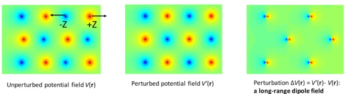
scat-+Z -Z
Unperturbed potential field V(r) Perturbed potential field V’(r) Perturbation ΔV(r) = V’(r)- V(r):
a long-range dipole field
Figure 1-1: The origin of the long-range dipole field due to LO phonon in polar material consisting two atoms per unit cell.
tering rate is written as[41],
1 𝜏𝑛k,𝑃 𝑂 = 𝑒 2𝜔 𝑜(𝜖∞−1− 𝜖0−1) ℎ√︀2𝜀𝑛k/𝑚*𝑑 [︃ 𝑁𝑜sinh−1 (︂ 𝜀𝑛k ¯ ℎ𝜔𝑜 )︂1/2 + (𝑁𝑜+ 1) sinh−1 (︂ 𝜀𝑛k ¯ ℎ𝜔𝑜 − 1 )︂1/2]︃ (1.46) where 𝑁𝑜 is the population of the longitudinal optical phonon.
1.4
A brief review of previous computational work
A full calculation of the thermoelectric transport properties using first principles is useful because it can provide insights, such as the electro/hole mean free paths, for experimentalists to optimize the thermoelectric performance of the materials. Such calculation is complicated as it is involved with numerous interdependent material parameters. Some intrinsic material parameters are difficult to extract from exper-iments, e.g. the lifetime of electrons. Previous computational works has to adopt certain level of assumptions to make the calculation of the transport properties. Constant relaxation time approximation. In Eq. 1.20, the lifetime of the carrier ap-pears in the numerator and the denominator at the same time, implying that the Seebeck coefficient might not be sensitive to the carrier lifetime given a weak enough dependence of lifetime on the wavevector. The electrical conductivity is closely re-lated to the carrier lifetime. The simplest treatment is to neglect the 𝑘-dependence of the carrier lifetime. A successful computational formalism named as BoltzTrap developed by Madsen and Singh[43] assumes a constant relaxation time for all
carri-ers and compute the transport properties based on the band structures from d ensity functional theory (DFT) on a highly dense 𝑘-point mesh. It turned out to be a good approximation for highly-doped semiconductors. For example, the Seebeck co-efficient of PbTe from calculation agrees well with experiments for different doping concentrations[64]. Based on results from such type of calculation, people also at-tributed the high Seebeck coefficient and high mobility of PbTe at the same time to the strongly corrugated shape of isoenergy surfaces[9].
The band structure calculation does not requires a lot of computation resource, making it possible to do a high-throughput calculation for various thermoelectric materials[24]. The disadvantage of this approach is that one has to assign a value for the lifetime to calculate the electrical conductivity. To the best of our knowledge, there is no report of first-principles calculation of the carrier lifetime in PbTe. Band structures beyond DFT at zero Kelvin. Considering the fact that the band gap rendered by DFT calculation is often underestimated, calculation beyond DFT could potentially improves the accuracy of the BoltzTrap calculation. In addition, the doping[18] and finite temperature could both modify the band structures thus the band structure from zero-Kelvin DFT calculation does not seem to be plausible. Svane et al. applied quasiparticle selt-consistent 𝐺𝑊 calculation to calculate the band gap and effective mass and achieved good agreement with experiments[68]. Gibbs et al. showed through ab initio molecular dynamics calculation in a supercell that the light band at L point and heavy band at Σ point converge at 700 K, consistent with optical measurements of the band gap. In 2014, Skelton et al. investigated the temperature effects on the band structures by giving specific lattice constants predicted using quasi-harmonic approximation (QHA)[65]. Although for each calculation, it is still zero-Kelvin calculation, they were able to obtain a more accurate band structure at finite temperatures.
Corrected k · p scheme for accurate band structures. The 𝐺𝑊 calculation of band structures is believed to be more accurate than DFT, yet the dramatically increased computational cost makes the computation on a fine 𝑘 mesh unachievable. In 2017, Berland et al. proposed a corrected scheme by solving the k · p method and
extrapo-lating the band structures from several 𝑘 points[5]. They demonstrate that not only the band structures, but the density of states as well as dielectric constant can be accurately extrapolated with computational cost on a sparse grid.
Fully first-principle calculation of electron transport in Si and GaAs. In 2015, Qiu et al. carried out the fully first-principle electron transport in silicon[58]. The electron-phonon scattering rate was calculated using electron-electron-phonon Wannier interpolation based on maximally localized Wannier functions and the electron mean free paths are reported. Unlike in non-polar silicon, the polarization scattering for electron can be significant in polar materials. In 2017, Liu et al. calculated the intrinsic electron life-time in GaAs within the relaxation life-time approximation[40]. They also calculated the electron mobility iteratively, achieving great agreements with experimental results. In practical thermoelectric materials, the ab initio calculation of electron transport is more complicated. For PbTe, it is known that the strong spin-orbit coupling leads to non-parabolic band structure, which requires a fully-relativistic calculation. Also, the screening effect of free carriers that affects the polar scattering should be considered.
1.5
Outline of the thesis
The goal of the thesis is to go beyond the constant relaxation time approximation and calculate the electron-phonon interaction rigorously. In Chapter 1, we have briefly reviewed previous computational efforts in calculating electrical transport properties using ab initio method. In Chapter 2, we first compactly introduce key assumptions in DFT. We review the density functional perturbation theory (DFPT) for the lat-tice dynamics calculation. In Chapter 3, we introduce the electron-phonon Wannier interpolation scheme to calculate the electron-phonon coupling matrix on a very fine grid. In Chapter 4, we present the ab initio electron mean free paths, electron trans-port properties and phonon transtrans-port properties in 𝑛-type PbTe. In Chapter 5, we summarize the findings and wisdom provided by calculation, and identify the future direction.
Chapter 2
Lattice dynamics from first principles
The density functional theory provides a parameter-free way towards the ground states of a electronic system. Phonon is considered as a perturbation to the ground states due to atom displacement. The 2𝑛+1 theorem states that the (2𝑛+1)𝑡ℎ deriva-tive of the eigenvalue of a Hamiltonian can be calculated with only the knowledge of the variance in the eigenfunctions up to order 𝑛[30]. In the sprit of 2𝑛 + 1 theorem, the density functional perturbation theory (DFPT) was proposed by Baroni[4] and Gonze[22] to calculate the phonon properties (first order) only requiring zeroth-order wavefunctions. In DFPT, the responses to perturbation is obtained by computing the system subject to external potential within the DFT formalism.
2.1
Density functional theory
Due to large mass difference between the ion and the electron, the Born-Oppenheimer approximation is considered to be a reasonable approximation to simplify the Schrödinger equation. Whenever the ion moves, the electron responds fast enough such that the ion is considered as fixed. This approximation allows us to construct the wavefunc-tion as Φ = 𝜑electron× 𝜑nuclei. The correlated nature of electrons in solids makes it
impossible to solve the many-body Schrödinger equation directly. A certain level of approximation needs to be adopted to obtain the electron eigenstates in the solids. The Hohenberg-Kohn theorem provides a new perspective to construct the equation
of motion for electrons in solids:
∙ Theorem 1 The external potential and the total energy is a unique functional of electron density 𝜌(r).
∙ Theorem 2 The ground state energy can be obtained variationally and the density that minimizes the total energy is the exact ground state density. For a very long time, scientists had struggled to find that functional of density. Even-tually, some approximated form of the functional is shown to be able to simplify the many-body Schrödinger equation to a set of one-electron equations and the reproduce the correct material properties.
2.1.1
Hartree approximation
The Hartree approximation states that the ansatz for the many-body electron wave-function may write as,
Φ(r1, r2, . . . , r𝑁) = 𝜑(r1)𝜑(r2) · · · 𝜑(r𝑁). (2.1)
Each particle is regarded as independent and interacts with each other through the mean-field Coulomb potential. The corresponding Schrödinger equation is,
[︂ − ¯ℎ 2 2𝑚∇ 2+ 𝑉 (r) ]︂ 𝜑𝑖(r) = 𝜀𝑖𝜑𝑖(r), (2.2)
where 𝑚 is the electron mass. The potential has two parts, the electron-nucleus interaction and electron-electron interaction, both in the form of Coulomb potential,
𝑉 (r) = −𝑍𝑒2∑︁ R 1 4𝜋𝜖0|r − R| − 𝑒2 ∫︁ dr′𝜌(r′) 1 4𝜋𝜖0|r − r′| , (2.3)
2.1.2
Hartree-Fock approximation
The Hartree approximation fails to capture the exchange interaction. The exchange interaction is due to the Pauli exclusion principle, which leads to antisymmetry when exchanging particle,
Φ(x1, x2, . . . , x𝑖, . . . , x𝑗, . . . , x𝑁) = −Φ(x1, x2, . . . , x𝑗, . . . , x𝑖, . . . , x𝑁), (2.4)
where x𝑖is the coordinate that includes position and spin. To satisfy such permutation
symmetry, one generalized form of the solution to the wavefunction is the Slater determinant, Φ(x1, x2, . . . , x𝑁) = 1 √ 𝑁 ! ⃒ ⃒ ⃒ ⃒ ⃒ ⃒ ⃒ ⃒ ⃒ ⃒ ⃒ ⃒ 𝜑1(x1) 𝜑2(x1) . . . 𝜑𝑁(x1) 𝜑1(x2) 𝜑2(x2) . . . 𝜑𝑁(x2) .. . ... . .. ... 𝜑1(x𝑁) 𝜑2(x𝑁) . . . 𝜑𝑁(x𝑁) ⃒ ⃒ ⃒ ⃒ ⃒ ⃒ ⃒ ⃒ ⃒ ⃒ ⃒ ⃒ . (2.5)
This leads the following Schrödinger equation, also know as the Hartree-Fock equa-tion, (︃ −¯ℎ 2 2𝑚∇ 2− 𝑍𝑒2∑︁ R 1 4𝜋𝜖0|r − R| −∑︁ 𝑗 𝑒2 ∫︁ dr′ |𝜑𝑗(r ′)|2 4𝜋𝜖0|r − r′| )︃ 𝜑𝑖(r) −∑︁ 𝑗 𝛿𝑠𝑖,𝑠𝑗𝑒 2 ∫︁ dr′𝜑 * 𝑗(r ′)𝜑 𝑖(r′) 4𝜋𝜖0|r − r′| 𝜑𝑖(r) = 𝜀𝑖𝜑𝑖(r) (2.6)
where 𝜑*𝑗(r′) is the complex conjugate of 𝜑𝑗(r′) and 𝑠𝑖 is the spin of the electron. The
last term in Eq. 2.6 describes the exchange interaction. However, the exchange term is a non-local operator for 𝜑𝑖 making the Hartree-Fock equation difficult to solve in
2.1.3
Kohn-Sham equation, local density approximation and
pseudopotentials
The Hartree-Fock equation include the exchange interaction, yet the correlation in-teraction is missed, which describes the influence on the movement of one electron by the presence of all other electrons. The key to resolve the issue is to modified the form of the effective potential. In 1965, Walter Kohn and Lu Jeu Sham[32] proposed a new way to include exchange-correlation interaction,
[︂ − ¯ℎ 2 2𝑚∇ 2+ 𝑉 eff(r) ]︂ 𝜑𝑖(r = 𝜀𝑖𝜑𝑖(r). (2.7)
The effective potential reads,
𝑉eff(r) = 𝑉ext(r) + 𝑒2 ∫︁ dr′ 𝜌(r ′) 4𝜋𝜖0|r − r′| + 𝛿𝐸xc[𝜌] 𝛿𝜌(r) , (2.8) where charge density 𝜌(r) =∑︀
𝑖|𝜑𝑖(r)|
2 and the last term is the exchange-correlation
potential. Later, the local-density approximation is proposed to provide a way to con-struct the correlation potential. In spin-unpolarized system, the exchange-correlation energy writes,
𝐸xc[𝜌] =
∫︁
dr𝜌(r)𝜀xc(𝜌), (2.9)
where 𝜀xc the exchange-correlation energy per particle of a homogeneous electron gas
with charge density 𝜌(r). The potential due to core valence electrons is included in 𝑉ext(r). The core is usually regarded as independent of the environment and can
be substituted by a pseudopotential. The pseudopotential replaces the Coulomb electron-ionic core interactions and it consists long-ranged local part and short-ranged non-local part,
𝑉𝑖 = 𝑉𝑛𝑙+ 𝑉𝑙𝑜𝑐, (2.10)
where 𝑖 represents 𝑖th ion. The long-ranged local part at a large distance to the ion center returns to the trivial Coulomb potential. Conversely, the short-ranged non-local part is written in terms of the sum of several angular-momentum dependent
potentials within the LDA,
𝑉𝑙𝑜𝑐(r) =
∑︁
𝑙
𝑉𝑙(𝑟) |𝑙⟩ ⟨𝑙| . (2.11)
In practice, the non-local pseudopotentials are written as a semilocal operator,
ˆ 𝑉𝑠𝑙 =
∑︁
𝑙𝑚
𝑉𝑙(𝑟)𝛿(𝑟 − 𝑟′)𝑌𝑙𝑚.(^r)𝑌𝑙𝑚* (^r′) (2.12)
where 𝑌𝑙𝑚 is the spherical harmonic function of degree 𝑙 and order 𝑚 defined in
spherical harmonics.
To be more specific, we carried out the first-principles calculation on electronic band structure using a 6 × 6 × 6 Monkhorst-Pack[50] 𝑘-grid with the cutoff energy of 70 Ry. We choose the norm-conserving fully relativistic pseudopotentials with local density approximation (LDA) for exchange-correlation energy functional. The calculation includes the spin-orbit coupling, implemented in Quantum ESPRESSO package[16]. The lattice constant used in calculation is 6.29 Å. The band gap given by the DFT calculation is 0.15 eV. As is known, the DFT-LDA suffers from underestimat-ing the material’s band gap. This is because the LDA has erroneous self-interaction: the exact exchange-correlation energy functional should cancel the self-interaction yet LDA does not. The LDA tends to over-delocalize the occupied states, leading to a higher energy of those states thus a smaller band gap[72]. In our case, we rigidly shift the conduction bands to match the band gap at room temperature, which is 0.316 eV[59]. The doping is modeled with a rigid band model approximation and dopants are assumed to be fully ionized in the whole temperature range in the calculation. Given the number of dopants, the chemical potential is obtained by solving the charge neutrality equation.
We would also like to address the effect of temperature on the band structure. There are several ways to calculate the band structure considering the temperature effect. The most straightforward way is the ab initio molecular dynamics[17]. We adopt the temperature-dependent band gap from experiment[59] and compare the
results with constant-band-gap calculation. We realize that the difference between the two cases is insignificant[1]. Consequently, we apply the same lattice constant and band gap for all calculations and the temperature effect is encoded in the distribution functions of electrons and phonons.
2.2
Density functional perturbation theory
The density functional theory provides a way to obtain the ground state energy. Based on linear response theory, the lattice vibration can be also studied by the density functional theory. The density functional-perturbation theory is the ab initio theory of lattice vibrations. Within the Born-Oppenheimer approximation, the Schrödinger equation that describes the lattice dynamics is,
[︂ −∑︁ 𝑖 ¯ ℎ2 2𝑀𝑖 𝜕2 𝜕R𝑖 + 𝐸(R) ]︂ Φion(R) = 𝜀Φion(R), (2.13)
where 𝑀𝑖 is the 𝑖th ion mass and R𝑖 is the position of its position. The 𝐸(R) is the
clamped-ion energy of the system composed of ion with fixed position and interacting electrons. The Hamiltonian to describe such system writes (in atomic unit),
𝐻BO(R) = − ¯ ℎ2 2𝑚 ∑︁ 𝑘 𝜕2 𝜕r2 𝑘 +𝑒 2 2 ∑︁ 𝑘̸=𝑗 1 |r𝑘− r𝑗| −∑︁ 𝑖𝑘 𝑍𝑖𝑒2 |r𝑘− R𝑖| +𝑒 2 2 ∑︁ 𝑖̸=𝑙 𝑍𝑖𝑍𝑙 |R𝑖− R𝑙| . (2.14)
The Hessian matrix scaled by the nuclear masses is,
M = 1
√︀𝑀𝑖𝑀𝑗
𝜕2𝐸(R)
𝜕R𝑖𝜕R𝑗
. (2.15)
And the phonon frequency is the eigenvalue of the Hessian matrix by,
det ⃒ ⃒ ⃒ ⃒ M − 𝜔2 ⃒ ⃒ ⃒ ⃒ = 0 (2.16)
To obtain the force, we refer to the Hellmann-Feynman theorem which states, 𝜕𝐸𝜆 𝜕𝜆 = ⟨ Ψ𝜆 ⃒ ⃒ ⃒ ⃒ 𝜕𝐻𝜆 𝜕𝜆 ⃒ ⃒ ⃒ ⃒ Ψ𝜆 ⟩ , (2.17)
where Ψ𝜆 is the eigenfunction of the Hamiltonian and 𝜆 is a parameter. Letting the
𝜆 to be the position r, we find that the force acting on 𝑖th nucleus is determined by,
F𝑖 = − 𝜕𝐸(R) 𝜕R𝑖 = ⟨ Ψ(R) ⃒ ⃒ ⃒ ⃒ − 𝜕𝐻BO 𝜕Ri ⃒ ⃒ ⃒ ⃒ Ψ(R) ⟩ . (2.18)
Then, the Hessian is represented by, 𝜕2𝐸(R)
𝜕R𝑖𝜕R𝑗
= −𝜕F𝑖 𝜕R𝑗
. (2.19)
2.2.1
Linear response theory
The essence of linear response theory is the transfer function that correlates the input and the output. In the case of lattice dynamics, the transfer function is the interatomic force constant that describes the energy variance upon atom displacement. In the realm of density functional theory, the perturbation due to atom displacement can be represented by the charge density. Based on the Hellmann-Feynman theorem, the first and seconder derivatives of the energy can be written as,
𝜕𝐸 𝜕𝜆𝑖 = ∫︁ 𝜕𝑉𝜆(𝜌) 𝜕𝜆𝑖 𝜌𝜆(r)dr, 𝜕2𝐸 𝜕𝜆𝑖𝜕𝜆𝑗 = ∫︁ 𝜕2𝑉 𝜆(r) 𝜕𝜆𝑖𝜕𝜆𝑗 𝜌𝜆(r)dr + ∫︁ 𝜕𝜌 𝜆(r) 𝜕𝜆𝑖 𝜕𝑉𝜆(r) 𝜕𝜆𝑗 dr. (2.20)
To calculate the force constant, the parameter 𝜆 is the position of the atom R. In the density functional theory formalism, the effective potential is also called self-consistent field (SCF) potential, 𝑉SCF= 𝑉ext(r) + 𝑒2 ∫︁ dr′ 𝜌(r ′) |r − r′| + 𝑣xc(r). (2.21)
2.2.2
General form of perturbed potential
Upon the perturbation, the perturbed potential to the lowest order is,
∆𝑉SCF(r) = ∆𝑉ext(r) + 𝑒2 ∫︁ dr′∆𝜌(r ′) |r − r′| + d𝑣xc(𝜌) d𝜌 ⃒ ⃒ ⃒ ⃒ 𝜌=𝜌(r) ∆𝜌(r). (2.22)
The lowest-order perturbed part of the eigenfunction is given by,
∆𝜓𝑛(r) = ∑︁ 𝑚̸=𝑛 𝜓𝑚(r) ⟨𝜓𝑚|∆𝑉SCF|𝜓𝑛⟩ 𝜀𝑛− 𝜀𝑚 . (2.23)
The corresponding perturbed part of the charge density is,
∆𝜌(r) = 4 𝑁/2 ∑︁ 𝑛=1 ∑︁ 𝑚̸=𝑛 𝜓𝑛*(r)𝜑𝑚(r) ⟨𝜓𝑚|∆𝑉SCF|𝜓𝑛⟩ 𝜀𝑛− 𝜀𝑚 . (2.24)
2.3
Phonons in polar materials
We have shown the force constant based on perturbation theory in first principles. To study phonons distinguished by wavevector and polarization, in particular, phonon dispersion, we need to construct the corresponding physical quantities in the recipro-cal space. Consider the Fourier transform of Eq. 2.22,
∆𝑉SCF(q) = 1 𝑉 ∫︁ ∆𝑉SCF(r)𝑒−𝑖q·rdr = ∆𝑉 (q) + 4𝜋𝑒2 𝑞2 ∆𝑛(q) + d𝑣𝑥𝑐 d𝑛 ∆𝑛(q). (2.25) This is a generalized perturbation potential as a function of wavevector 𝑞. We also need to obtain the force constant in the reciprocal space. If the position of 𝑖th atom is,
R𝑖 = R𝑙+ 𝜏𝑠+ u𝑠(𝑙), (2.26)
where R𝑙 is 𝑙th lattice site, 𝜏𝑠 is the equilibrium position of 𝑠th atom relative to 𝑙th
lattice site and u𝑠(𝑙) is the deviation of the 𝑠th atom from its equilibrium.
𝑗th atom is, 𝐶𝑠𝑡𝛼𝛽(𝑙, 𝑚) = 𝜕 2𝐸 𝜕𝑢𝛼 𝑠(𝑙)𝜕𝑢 𝛽 𝑡(𝑚) = 𝐶𝑠𝑡𝛼𝛽(R𝑙, R𝑚). (2.27)
The Fourier transform of the force constant reads,
̃︀
𝐶𝑠𝑡𝛼𝛽(q) =∑︁
𝑅
𝑒−𝑖q·R𝐶𝑠𝑡𝛼𝛽(R), (2.28) where we take advantage of the translational symmetry and simplify the real-space force constant to be 𝐶𝑠𝑡𝛼𝛽(R𝑙, R𝑚) = 𝐶𝑠𝑡𝛼𝛽(R). The phonon eigenfrequencies are
ob-tained by solving the equation,
det ⃒ ⃒ ⃒ ⃒ 1 √ 𝑀𝑠𝑀𝑡 ̃︀ 𝐶𝑠𝑡𝛼𝛽(q) − 𝜔2(q) ⃒ ⃒ ⃒ ⃒ = 0. (2.29)
In polar materials, the long-range polarization field as described by Eq. 1.43 leads to a force constant that cannot be defined through Fourier transform as in the long wavelength limit, the force constant diverges. Such divergence can be resolved by adding a correction term — the nonanalytic force constant.
2.3.1
Nonanalytical force constant in polar materials
The Born effective charge is a tensor defined by,
𝑒𝑍*𝛼𝛽𝑠 = Ω 𝜕P𝛼 𝜕𝑢𝛽𝑠(q = 0) ⃒ ⃒ ⃒ ⃒ E=0 , (2.30)
where 𝑃𝛼 is the polarization vector due to atom displacements. In first-principle
calculation, the polarization per unit cell is written as,
𝑃𝛼 = 1 Ω ∑︁ 𝑠,𝛽 𝑒𝑍𝑠*𝛼𝛽𝑢𝑠,𝛽+ 𝜖𝛼𝛽 ∞ − 𝛿𝛼𝛽 4𝜋 𝐸𝛽. (2.31)
Another important quantity that is related to the polarization is the high-frequency electronic dielectric constant tensor,
𝜖𝛼𝛽∞ = 𝛿𝛼𝛽 + 4𝜋 𝜕𝑃𝛼 𝜕𝐸𝛽 ⃒ ⃒ ⃒ ⃒ u𝑠(q=0)=0 , (2.32)
where 𝛿𝛼𝛽 is Kronecker delta. With the Born effective charge and dielectric constant
being defined, the nonanalytic force constant writes,
na𝐶˜𝛼𝛽 𝑠𝑠′(q) = 4𝜋 Ω𝑒 2(q · Z * 𝑠)𝛼(q · Z*𝑠′)𝛽 q · 𝜖∞· q . (2.33)
In cubic systems, the transverse phonon mode does not induce long-range electrical field yet the longitudinal phonon mode does. Thus, the phonon frequency of lon-gitudinal optical phonon mode is usually higher than the transverse optical phonon mode. In cubic materials, the longitudinal phonon frequency is,
𝜔LO = √︃ 𝜔2 TO+ 4𝜋𝑒2𝑍*2 Ω𝜖∞𝑀 . (2.34)
The frequency difference between longitudinal optical phonon and transverse optical phonon near Γ point in the Brillouin zone is named as LO-TO splitting. The nonan-alytical force constant makes sure the correct LO-TO splitting in phonon dispersion.
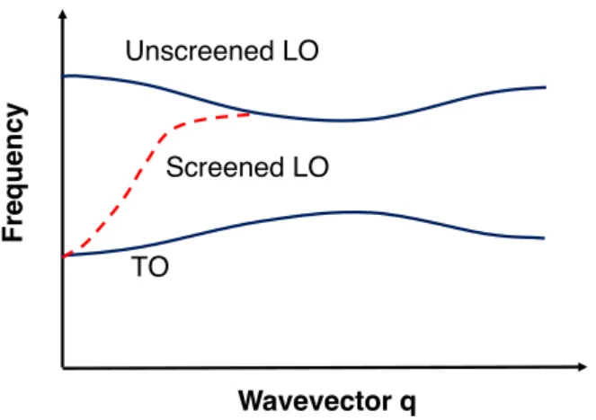
2.3.2
The screening effect of free carriers on phonons
In highly-doped semiconductors, the free carriers can respond to the polarization generated by the ion. Effectively, the long-range electrical field that leads to LO-TO splitting is screened, shown in Fig. 2-1. To include the screening effect in our calculation, we will derive the correction term for the nonanalytical force constant. The Lindhard dielectric function, as derived in Appendix A, is,
𝜖(𝑞) = 1 + 1 2 𝑘𝑇 𝐹2 𝑞2 + 1 2 𝑘2𝑇 𝐹 𝑞2 𝑘𝐹 𝑞 (︂ 1 − 𝑞 2 4𝑘2 𝐹 )︂ ln ⃒ ⃒ ⃒ ⃒ 2𝑘𝐹 + 𝑞 2𝑘𝐹 − 𝑞 ⃒ ⃒ ⃒ ⃒ (2.35)
Unscreened LO TO Screened LO Fre que nc y Wavevector q
Figure 2-1: The screening effect of free carriers on the optical phonon modes. At the limit of 𝑞 → 0, the LO and TO modes converges given strong enough screening effect
where the Thomas-Fermi wavevector is defined by,
𝑘2TF = 𝑒 2 𝜖0𝜖∞ 𝜕𝑛 𝜕𝐸𝐹 = − 𝑒 2 𝜖0𝜖∞ ∫︁ 𝑔(𝜀)𝜕𝑓 𝜕𝜀d𝜀. (2.36)
In the parabolic band model, the Thomas-Fermi wavevector can be expressed as 𝑘𝑇 𝐹 =
√︁
𝑒2𝑛
𝜖0𝜖∞𝑘𝐵𝑇. From Fig. 2-2, we find that the using the density of states from
DFT calculation renders similar screening radius. The discrepancy is attributed to the non-parabolic nature of the band structures of PbTe. The 𝑘𝐹 in Eq. 2.35 is the
Fermi velocity. Equivalently,
𝜖𝐿(𝑞) = 1 + 𝑘2 𝑇 𝐹 𝑞2 [︃ 1 2 + 1 − 𝑥2 4𝑥 ln ⃒ ⃒ ⃒ ⃒ 1 + 𝑥 1 − 𝑥 ⃒ ⃒ ⃒ ⃒ ]︃ (2.37)
where 𝑥 = 𝑞/2𝑘𝐹. Till now, the band is assumed to be parabolic, the Fermi energy
should be much larger than 𝑘𝐵𝑇 . In fact, we find in PbTe that only small |q| can lead
to strong Fröhlich interaction thus the choice of dielectric constant at large |q| would not affect the accuracy of the transport calculation. Furthermore, we argue that for those LO phonons that induce POP scattering, the phonon wavevector satisfies |q| ≪ 2𝑘𝐹 in highly-doped PbTe. In such conditions, the Lindhard dielectric can be
Figure 2-2: The inverse of the Thomas-Fermi wavevector (1/𝑘𝑇 𝐹) — screening
radius as a function of carrier density from DFT and from parabolic band model.
further reduced to Thomas-Fermi screening model,
𝜖(𝑞) = 𝜖∞ (︂ 1 + 𝑘 2 𝑇 𝐹 𝑞2 )︂ , (2.38)
where 𝜖∞is ion-clamped (high frequency) macroscopic dielectric constant from DFPT[23][53].
After plugging in the dielectric constant in Eq.2.38 into Eq. 2.33, we can express the screened long-range force constant as,
na𝐶˜𝛼𝛽 𝑠𝑠′(q) = 4𝜋 Ω𝑒 2(q · Z * 𝑠)𝛼(q · Z*𝑠′)𝛽 |q|2𝜖 ∞(1 + 𝑘2 𝑇 𝐹 𝑞2 ) . (2.39)
2.3.3
Phonon dispersion of PbTe with different carrier
con-centrations
The force constant in Eq. 2.28 is defined on a uniform q-point mesh in standard DFPT calculation. To capture the long-range feature of LO phonon, we directly subtract the force constant with nonanalytical force constant described by Eq. 2.33 to obtain
a purely short-range force constant. Then, we add back the screened long-range force constant in Eq. 2.39 to examine the case the excess free carriers due to doping. In the calculation, we use a 6 × 6 × 6 𝑞-point mesh. In order to match the bulk phonon dispersion with neutron scattering, a Born effective charge of 𝑍* = 5.8 and a dielectric constant of 32 from Ref.[36] are adopted.
We demonstrate the consequence of the screening effect: the weakened LO-TO splitting, by calculating the phonon dispersion with various carrier concentrations. In Fig. 3-4 (c), we clearly observe that as the carrier concentration increases, the gap between LO and TO phonons near zone center is progressively narrowed. In the high-carrier-concentration limit and the long-wavelength limit, one should no longer be able to distinguish a LO and TO phonon since the screening length has becomes so small that the long-range dipole field responsible for the LO-TO splitting vanishes. The convergence of long-wavelength LO and TO phonon reminds us to examine whether it gives rise to stronger anharmonicity since TO phonon contributes remarkably to phonon-phonon scattering in PbTe[12]. However, we do not observe any noticeable difference after carrying out thermal conductivity calculation, because an only small fraction of LO phonons become TO phonons such that the three-phonon scattering phase space is barely modified.
K ! X W ! L 0 20 40 60 80 100 120 140 Phonon frequency (cm -1 ) Neutron scattering 1.0 x 1017 cm-3 2.3 x 1019 cm-3 9.4 x 1019 cm-3 Bulk
Without screening With screening
(c)
(a) (b)
Figure 2-3: The phonon dispersion for different free carrier concentrations compared with neutron scattering experiment[10].
Chapter 3
Electron-phonon interaction in from
first principles
The electron-phonon interaction is a fundamental type of interaction in solids that significantly influences the transport of electrons. The superconductivity, Joule heat-ing, thermal relaxation of electrons, Raman spectroscopy et al. are all closely related to phonon interaction. Despite a very long history of study of electron-phonon interaction, an accurate, fully first-principle formalism was not accessible until recently, as the dimensions of the quantity of interest is huge. Thus, the ab initio electron-phonon coupling calculation can be computationally infeasible. In this Chapter, we will introduce a scheme named electron-phonon Wannier interpolation which allows us to calculate electron-phonon interaction with relatively low cost and high accuracy.
3.1
Electron-phonon interaction to the lowest order
The Hamiltonian of a coupled electron-phonon system is[20]:
ˆ 𝐻 =∑︁ 𝑛k 𝜀𝑛k𝑐ˆ † 𝑛kˆ𝑐𝑛k+ ∑︁ q𝜈 ¯ ℎ𝜔q𝜈(︀ˆ𝑎†q𝜈ˆ𝑎q𝜈+ 1/2 )︀ + 𝑁𝑝−1/2∑︁ k,q 𝑚𝑛𝜈 𝑔𝑚𝑛𝜈(k, q) ˆ𝑐 † 𝑚k+q𝑐ˆ𝑛k (︁ ˆ 𝑎q𝜈 + ˆ𝑎 † −q𝜈 )︁ + [︃ 𝑁𝑝−1 ∑︁ k,q,q′ 𝑚𝑛𝜈𝜈′ 𝑔DW𝑚𝑛𝜈𝜈′(k, q, q′) ˆ𝑐 † 𝑚k+q+q′ˆ𝑐𝑛k (︁ ˆ 𝑎q𝜈 + ˆ𝑎 † −q𝜈 )︁ (︁ ˆ 𝑎q′𝜈′ + ˆ𝑎† −q′𝜈′ )︁ ]︃ , (3.1)
where 𝜀𝑛k is the eigen-energy of a electron state with wavevector k in the branch 𝑛,
while 𝜔q𝜈 is the frequency of a phonon state with wavevector q in the branch 𝜈. The
creation operator ˆ𝑐†𝑛k creates an electron state |𝑛k⟩︀ and the annihilation operator annihilates an electron state |𝑛k⟩︀. Similarly, the creation operator ˆ𝑎†
q𝜈 creates a
phonon state |q𝜈⟩︀ and the annihilation operator ˆ𝑎†q𝜈 annihilates a phonon state |q𝜈⟩︀. 𝑁𝑝 is the number of unit cells in a periodic supercell. In the first line of the equation,
electrons and phonons are described separately. The second line of the equation corresponds the electron-phonon coupling to the first order of the atom’s lifetime displacements[44]. The third line of the equation describes the higher-order electron-phonon interaction.
The electron-phonon coupling matrix to the lowest-order approximation is given by, 𝑔𝑚𝑛𝜈 (k, q) = (︂ ¯ ℎ 2𝑚0𝜔𝜈q )︂12 ⟨ 𝜓𝑚k+q ⃒ ⃒ ⃒ 𝜕𝑉SCF 𝜕u𝜈q · e𝜈q ⃒ ⃒ ⃒𝜓𝑛k ⟩ , (3.2)
where 𝑚0is the electron rest mass, 𝜓𝑛kis the electron wavefunction. The lowest-order
electron-phonon interaction is responsible for the broadening of the electron states (i.e. the finite lifetime of electrons). 𝜕𝑉SCF/𝜕u𝜈q·e𝜈qis the first-order variation of the
self-consistent potential energy due to the presence of a phonon, as depicted Eq. 2.22 in Chapter 2.
by, 𝑔𝑚𝑛𝜈𝜈DW ′(k, q, q′) = ¯ ℎ 2𝑚0𝜔𝜈q𝜔𝜈′q′ ⟨ 𝜓𝑚k+q+q′ ⃒ ⃒ ⃒ 𝜕𝑉SCF 𝜕u𝜈q · e𝜈q 𝜕𝑉SCF 𝜕u𝜈′q′ · e𝜈′q′ ⃒ ⃒ ⃒𝜓𝑛k ⟩ . (3.3)
It is believed that Debye-Waller term is responsible for the band energy renormal-ization: at high temperatures, the electronic bands can be significantly modified by the electron-phonon interaction. In narrow-band-gap thermoelectric materials like PbTe, the band gap is strongly dependent on temperature due to Debye-Waller type of electron-phonon scattering[63]. The higher-order coupling is complicated to be computed and beyond the scope of this thesis.
3.2
Electron-phonon Wannier interpolation
The energy of electrons is around several eV, while the energy of phonons is in meV scale. The phonon absorption where 𝑛k + 𝜈q → 𝑚k′ requires that the momen-tum is conserved with discrete translational symmetry: k + q = k′ + G (G is the reciprocal lattice vector). More importantly, the energy conservation requires 𝜀𝑛k + ¯ℎ𝜔𝜈q = 𝜀𝑚k′. Similarly, the phonon emission process where 𝑛k → 𝜈q + 𝑚k′
requires that k = q + k′ + G and 𝜀𝑛k = ¯ℎ𝜔𝜈q + 𝜀𝑚k′ Due to the large mismatch
in energy between electrons and phonons, a very dense 𝑘-point mesh is needed for direct calculation in the search of possible electron-phonon scattering modes such that energy and momentum conservation can be satisfied. The resultant severe com-putational challenge demands alternative approaches to obtain the electron-phonon coupling matrix.
3.2.1
Maximumly localized Wannier function
In periodic solids, the translational symmetry leads to the Bloch’s theorem where the Bloch orbitals are Bloch amplitude multiplied by the phase which extends to the whole material. The Bloch orbitals are eigenstates of Hamiltonian. The Wannier function, localized in real space, is transformed from Bloch orbital[47]. For Bloch function, each
orbital is marked with a k and it has a well-defined energy. For Wannier function, however, we cannot find the energy level of the orbital as it is a band. Thus we say we the localization in real space of Wannier function is achieved by losing localization in energy.
The Wannier function is defined by unitary transform (preserving the length of a vector), ⃒ ⃒𝑚R𝑒⟩︀ = ∑︁ 𝑛k 𝑒−𝑖k·R𝑈𝑛𝑚,k ⃒ ⃒𝑛k⟩︀, (3.4)
where 𝑈𝑛𝑚,k is a unitary matrix. The plane wave basis can be recovered through
inverse Fourier transform,
⃒ ⃒𝑛k⟩︀ = 1 𝑁𝑒 ∑︁ 𝑚R 𝑒−𝑖k·R𝑈𝑛𝑚,k† ⃒⃒𝑚R𝑒⟩︀. (3.5)
The idea of the Wannier function is to find an alternative basis to replace plane wave basis. Since the number of Wannier functions per unit cell is the number of electrons per unit cell, much smaller than the number of plane waves typically used in DFT calculation, the computational cost can potentially be reduced. Apparently, the uni-tary transformation is not unique, as long as the Wannier functions are orthogonal. A localization criterion is proposed by Marzari and Vanderbilt[47] to obtain the max-imumly localized Wannier function iteratively. The localization functional is defined by, Ω =∑︁ 𝑛 [︂ ⟨︀𝑛0|𝑟2|𝑛0⟩︀ − ⟨𝑛0|𝑟|𝑛0⟩2 ]︂ . (3.6)
This quantity is actually the quadratic spreads of Wannier function around their cen-ters in the home unit cell. By minimizing the localization functional through refining the unitary matrix 𝑈𝑛𝑚,k, we are able to obtain the maximumly localized Wannier
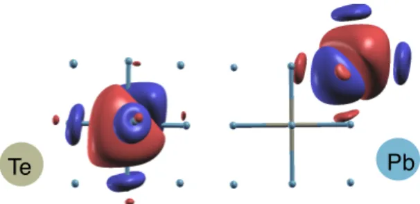
function. The Wannier function can be calculated using Wannier90[51] package once we have the Bloch orbitals from DFT calculation. In Fig. 3-1, the maximumly local-ized Wannier functions of Pb and Te atom in PbTe are shown. Different color of the isosurface (iso-charge-density) indicates the opposite sign of the values of Wannier orbitals. The shape of isosurface displays the character of 𝜎-bounded combination of

![Figure 2-3: The phonon dispersion for different free carrier concentrations compared with neutron scattering experiment[10].](https://thumb-eu.123doks.com/thumbv2/123doknet/13812194.441887/44.918.249.654.394.729/figure-dispersion-different-carrier-concentrations-compared-scattering-experiment.webp)