Advanced Silicon Photonic Microcavities for Routing,
Detection and Lasing Applications
by
Zhan Su
S.M. (Electrical Engineering and Computer Science) Massachusetts Institute of Technology (2013)
Submitted to the Department of Electrical Engineering and Computer Science in partial fulfillment of the requirements of the degree of
Doctor of Philosophy in Electrical Engineering at the
MASSACHUSETTS INSTITUTE OF TECHNOLOGY February 2017
© Massachusetts Institute of Technology 2016. All rights reserved.
Author . . . .
Department of Electrical Engineering and Computer Science
December 6, 2016
Certified by . . . .
Michael R. Watts
Associate Professor of Electrical Engineering
Thesis Supervisor
Accepted by . . . .
Leslie A. Kolodziejski
Professor of Electrical Engineering
Chair, Department Committee on Graduate Students
Advanced Silicon Photonic Microcavities for Routing,
Detection and Lasing Applications
by
Zhan Su
Submitted to the Department of Electrical Engineering and Computer Science on December 6, 2016, in partial fulfillment of the
requirements of the degree of
Doctor of Philosophy in Electrical Engineering
Abstract
The theoretical background of microcavities for photonic applications has been extensively investi-gated in theory over the past two decades. These structures provide the ability to filter wavelength, support high-Q modes and enhance intensity within the cavities while maintaining a small device footprint. Such characteristics make these structures good candidates to optimize performance and shrink the size of devices for both linear and nonlinear optics. Recent advancements in silicon-based fabrication technology provide access to dopants for active control, material layers such as germa-nium and silicon nitride, and 3D-integration technologies that were previously exclusive to electronics development, leading to tremendous progress in cavity-based integrated photonic circuits.
Using the silicon photonic platform developed by our group, high-performance microcavity-based structures have been demonstrated for optical signal routing, detection, and lasing applications. We first introduce partial-drop filters and present results using them to achieve a highly uniform wavelength-division-multiplexing (WDM) compatible optical multicast system. We then implement a waveguide-coupled resonant detector using a germanium layer grown on top of the silicon. In addition to having low dark current and high-speed performance, the resonant detector extends the wavelength detection range beyond 1620nm while maintaining a device radius only 4.5µm. Fur-thermore, an easy-to-fabricate waveguide-coupled trench-based Al2O3microcavity is presented that
achieves a Q-factor on the order of 106 with a bend radius on the scale of 100µm. Compact on-chip
rare-earth-ion (ytterbium, erbium, thulium) doped Al2O3 lasers were then demonstrated with a
sub-milliwatt lasing threshold, making trench-based cavities a suitable platform to achieve optically pumped on-chip lasers.
Thesis Supervisor: Michael R. Watts
Preface and Acknowledgement
The past five and a half years at MIT have been a great experience in my life. During the period, I have not only gained knowledge on the research I have been focusing on but also learned how to work in a team and lead projects when I became more experienced.
First and foremost, I was privileged to have the opportunity to join Prof. Michael R. Watts’s group. The day when I received his response that I can join his team is one of the best moment in my life. Over the past five and a half years, under his lead, we started with a small group with a little amount of equipment to a big lab with plenty of resources. His visions and passions on electronics-photonics 3D integration and on-chip laser designs provided us with great motivations and further guide the silicon photonics research into practical industrialization. BBQ and fishing trip during summer and Fire and Ice get-together during Christmas have been great memories shared by all the group members.
I am also grateful to have Prof. Erich P. Ippen on my thesis committee. Listening to his comments during project meeting and witnessing those moments when ideas came so naturally from him have been a great experience in my Ph.D. life. His en-couragement and suggestions during my thesis committee meeting and thesis writing process helped me better understand the physics behind my thesis topics.
I would also like to thank Prof. Qing Hu for being one of my committee members. The time I spent in his 6.730 class during my first year not only helped me with a better understanding of solid-state physics but also provided me with a chance to collaborate with other students, who later have become my great friends and strong supports through my Ph.D. life.
I also want to thank Dr. Erman Timurdogan for his help over the past few years. I am very grateful to be his officemate and labmate. The days we spent together discussing technological designs and experiments gave us not only a deeper under-standing of our research topics but also a great friendship. As a student who joined the group one year earlier than me, he helped me from the beginning of electromag-netic FDTD simulation and Cadence mask layout to further collaboration work on electronics-photonics integration. It has been a great experience to work
back-to-back in the same office, go to different places (Stata Center first floor, ground floor, student center, Starbucks in Kendall Square) for the same coffee during weekdays or sometimes weekends. Also, while getting a Ph.D. needs a lot of patience, as a life-long friend, he can always give me useful advice on dealing with different situations from his experience.
I would also like to thank my colleague Dr. Jie Sun for his help. As a pioneer in phased array in our group, he has left a rich and great legacies that laid down the foundation of silicon photonic phased array. I am so grateful to be his officemate and had the chance to work with him on a variety of research topics. His advice on research and future jobs have helped me figuring out what I want to achieve from my Ph.D. works.
I also want to thank Dr. Jonathan D. B. Bradley (now Prof. Bradley) for his great help in guiding my research. I am particularly impressed by his dedication to research. Getting a fabrication system up and running requires great effort. I was grateful to have worked with him on thulium laser development and seeing my thulium microcavity laser design worked from his film deposition was one of the greatest moment during my Ph.D. research.
MIT has been a great place to conduct research not only because of the abun-dant technical resources on campus but also talent people around me. I also want to thank my labmates Christopher Poulton, Manan Raval, Matthew Byrd, Jelena Notaros, Diedrik Vermeulen, Patrick Callahan, Katia Shtyrkova, Michele Moresco, Ehsan Hosseini, Purnawirman, Jerry Zhou, Nanxi Li, Salih Magden, Neetesh Singh, Alfonso Ruocco, Ami Yaacobi, David Cole, Anna Baldycheva, Cheri Sorace-Agaskar, and Aleksandr Biberman for all the time that they have spent with me.
In addition, I want to thank people from other groups, Guolong Su, Jinshuo Zhang, Ningren Han, Huaiyu Meng, Shengxi Huang, Tao Yu, Yang Yang, Qiu Xin, Xun Cai, Yichen Shen, Bo Zhen, Hung-Wen Chen, Duo Li, Hangbo Zhao, Longwu Ou, David Burghoff, Karan Mehta, Amir Atabaki and Luca Alloatti, for useful discussions and allowing me to borrow their equipment for experiment.
Last but not least, I would like to thank my wife and my parents for their constant support and consideration. Thanks for bringing the sunshine into my life and making
Contents
1 Introduction 25
1.1 Foundry-Based Silicon Photonics . . . 26
1.2 Microcavities . . . 30
1.3 Outline of this Thesis . . . 32
2 Optical Routing and Multicasting Systems 34 2.1 Introduction . . . 35
2.2 1st-Order Optical Multicasting System . . . 36
2.2.1 Theory – Single Device . . . 36
2.2.2 Theory – Cascaded System . . . 39
2.2.3 Experimental Implementation . . . 41
2.2.4 Conclusion . . . 47
2.3 Unicast and Multicast Network in a Ring-Based Photonic System . . 47
2.3.1 Device Schematic . . . 48
2.3.2 Device Characterization . . . 49
2.3.3 Conclusion . . . 52
2.4 2nd-Order Optical Multicasting System . . . 52
2.4.1 Theory – Single Device . . . 53
2.4.2 Theory – Cascaded System . . . 55
2.4.3 Experimental Implementation . . . 58
2.4.4 Conclusion . . . 59
2.5 Extension to Higher-Order Filter-Based Structure . . . 61
3 Resonant Germanium-on-Silicon Detector 64 3.1 Introduction . . . 65
3.2 Theories and Simulations . . . 65
3.3.1 Device Fabrication and Passive Cavity Calibration . . . 70
3.3.2 Dark Current and Responsivity . . . 73
3.3.3 High Speed Testing . . . 77
3.4 Applications in Multicasting System . . . 78
3.5 Conclusion . . . 81
4 Microcavity Laser Sources 82 4.1 Microcavity Simulation and Fabrication Flow . . . 83
4.2 Passive Microcavity . . . 86
4.2.1 Silicon Nitride Loss Test . . . 87
4.2.2 Passive Al2O3 Cavity Measurement . . . 89
4.2.3 Discussion . . . 98
4.2.4 Conclusion . . . 99
4.3 Thulium Laser . . . 99
4.3.1 Al2O3:Tm3+ Deposition . . . 100
4.3.2 Thulium Amplified Spontaneous Emission Spectrum . . . 102
4.3.3 Thulium Film Absorption . . . 103
4.3.4 Microcavity Designs and Transmission Spectrum . . . 104
4.3.5 Lasing Spectrum . . . 107
4.3.6 Pumping with a 780nm Laser Diode . . . 111
4.3.7 Conclusion . . . 113
4.4 Ytterbium Laser . . . 113
4.4.1 Mode Profiles and Mode Overlap . . . 115
4.4.2 Experimental Results . . . 117
4.4.3 Conclusion . . . 119
5 Wafer-Scale Robust High-Q Microcavity Design 120 5.1 Introduction to Adiabatic Microring Resonator . . . 121
5.2 Reduced Wafer-Scale Variation Sensitivity – Simulation . . . 122
5.3 Reduced Wafer-Scale Variation Sensitivity – Experiment . . . 124
5.4 High-Q Cavity with Contacts . . . 127
6 Conclusions 130
Appendices 133
A Quality Factor Definition and Related Calculations . . . 133
B Quality Factors Extraction . . . 136
C Microcavity Laser Performance Estimation . . . 144
D Modulator Power Consumption Comparison . . . 147
List of Publications 150
List of Figures
1.1 (a) Silicon layer with dopants of different types (p- or n-type) and concentrations for applications such as modulators or tunable filters. (b) Germanium on silicon layer for photodetection applications. (c) Two silicon nitride layers (nitride 1 and nitride 2) with a deep trench on top for the on-chip optically pumped laser development. . . 27
1.2 Masks taped out during my Ph.D. study. . . 28
1.3 A gallery of silicon photonic devices fabricated in the platform developed by MIT and SUNY Polytechnic Institute. Top-view SEMs were taken after a reactive-ion-etching (RIE) of the SiO2
cladding material. (a) A second-order tunable microring filter. (b) Two microdisk modulators. (c) A waveguide-coupled Ge-on-Si photodetector. (d) The cross-section of a microcavity laser. (e) A two-dimensional phased array with a dynamic thermal tuning. (f) A microring-based optical broadcast/multicast system. (g) A grating
coupler. (h) A set of cadcaded thermal phase shifters. . . 29
1.4 An illustration of a waveguide-coupled microcavity used as a channel-dropping filter. . . 30
1.5 An illustration of a waveguide-coupled microcavity used as an high-efficiency absorber. Qi denotes the intrinsic Q-factor of the cavity
and Qe represents the external Q-factor. When Qi = Qe, full power
absorption can be achieved when the input wavelength matches one
of the resonances in the cavity. . . 31
1.6 An illustration of optical intensity enhancement using a microcavity
2.1 (a) An example approach of using wavelength selective partial drop filters in an all-to-all communications network. (b) A simplified 1-by-8 on-chip broadcast network. Inset: Implementation of resonant detector at wavelength λ1. . . 36
2.2 A schematic of a single-ring-based filter. . . 37
2.3 2D FDTD simulations of microring-based filters with (a) a symmetric coupling configuration and (b) an asymmetric coupling configuration. 37
2.4 A coupled-mode-theory (CMT) model of a microring filter. . . 38
2.5 A schematic of an N -stage ring-based cascaded partial-drop filter system. Each ring supports a circulating mode with energy amplitude A, incident wave amplitude S1+, transmitted wave amplitude S1−,
drop port output wave amplitude S2−, and input wave amplitude S2+.
τ denotes the amplitude decay time constant of each cavity due to the coupling to a separate waveguide. . . 40
2.6 Quality factors calculated from the coupled-mode-theory to maintain an equal power distribution in an eight-stage partial-drop filter bank. 41
2.7 (a) A schematic of a tunable adiabatic microring resonator. (b) The transmission spectra of a 3µm-radius adiabatic microring resonator under different bias voltages, showing a clean free-spectra-range (FSR). (c) Power consumption of the integrated heater vs. resonant
frequency shift, showing a thermal tuning efficiency of 6.3µW/GHz. . 42
2.8 (a) A schematic of the optical multicast system. All the microrings shown in the figure have the same resonant frequency with different couplings to the bus and drop waveguide. (b) A scanning electron micrograph (SEM) of the fabricated device. Inset: a close-up view of the fabricated tunable adiabatic microring filter. . . 43
2.9 (a) Transmission spectra of the 1-by-8 multicasting system before thermal tuning. (b) Tuning power of each drop port. (c) Transmission spectra of the multicasting system after thermal tuning. Inset: spectral response of the device showing an uncorrupted 36.2nm free-spectral-range. (d) Close-up view of the transmission spectra of the multicasting system after thermal tuning, showing a power variation
of 0.11dB on resonance with 2.96mW total tuning power. . . 44
2.10 (a) A diagram of the experimental setup for characterizing the data transmission performance. (b) Eye-diagrams for drop ports 1 to 8 with 10Gbit/s data rate generated from external commercial LiNbO3
modulator with input laser wavelength at 1554nm. . . 45
2.11 Experimentally measured bit-error-rate (BER) curves for the partial drop broadcast system for each drop port with a 10Gbit/s data rate
generated from an external commercial LiNbO3 modulator. . . 46
2.12 (a) A schematic of the ring-based wavelength unicast and multicast network. The wavelengths (λ1 to λ4) on the side of the rings denote
the resonances of the corresponding microring resonators. (b) An
illustration of the functions of the system. . . 48
2.13 (a) Transmission spectra of the tunable interior-ridge microring resonator with different applied voltages. (b) Tuning power, frequency shift and device resistance for various applied voltages. (c) Thermal
frequency shift vs. thermal tuning power. . . 49
2.14 (a) Transmission spectra of In1 to output ports 1, 3 and 4. (b)
Transmission spectra of In2 to output ports 2, 3 and 4. . . 50
2.15 (a) A schematic of the high-speed data transmission measurement system. (b) Eye diagrams of different routing/multicasting function of the designed network. (c) Experimentally measured bit-error-rate (BER) curves for all configurations of the developed system with 10Gbit/s data rates generated from an external commercial LiNbO3
2.16 Frequency responses of drop ports of different orders of ring-based filters with frequency offset normalized to 3dB bandwidth based on
the coupled-mode-theory theory. . . 53
2.17 A schematic of the CMT model of a second-order filter. . . 54
2.18 Simulated transmission spectra of thru ports and drop ports for both a lossless full-drop filter and a partial-drop filter with the same Full-Width Half-Maximum (FWHM) bandwidth and 1/8 power splitting
ratio on resonance. . . 54
2.19 A schematic of an N -stage second-order ring-based multicasting system. 56
2.20 (a) A scanning electron micrograph (SEM) of the fabricated device after a dry etching to remove the top SiO2 cladding. (b) A zoom-in of
the first stage (red dashed box in (a)). (c) A zoom-in of the last stage (solid cyan box in (a)). . . 59
2.21 (a) The transmission spectra of port Thru and Drop1 of the designed 1-by-8-port 2nd-order multicast filter bank. Simulated port Drop1 responses for both 1-by-8-port 1st-order and 2nd-order multicast filter bank with the same FWHM bandwidth are included for comparison. Nearby frequency channels with < -25dB crosstalk level are marked with 1 and 2 for 1st-order and 2nd-order system, respectively. (b) Transmission spectra of the thru and eight drop ports of the 2nd-order partial-drop filter bank after thermal tuning. (c) A zoom-in of the transmission spectra of the system (marked by a dashed box in (b)), showing a power variation of 1/4dB at the resonant wavelength. . . . 60
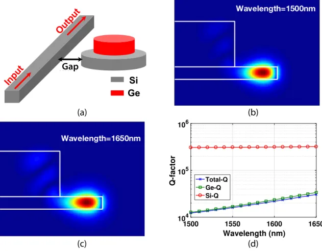
3.1 Imaginary components of the germanium refractive indices for wave-length from 1.4-1.8µm in Ref. [66]. . . 66
3.2 (a) A schematic of the proposed waveguide-coupled germanium-on-silicon photodetector. (b) Fundamental mode (TE11) at λ = 1500nm.
(c) Fundamental mode (TE11) at λ = 1650nm. (d) Calculated
total intrinsic Q -factors for wavelengths from 1500 to 1650nm. Contributions from the Ge absorption and silicon absorption to the
3.3 (a) A schematic of a waveguide coupled to a microdisk for FDTD simulations. (b) Coupling strengths vs. coupling gap sizes and
wavelengths. . . 69
3.4 Coupling Q -factor (Qe) for different ring-bus separations and
wave-lengths. . . 69
3.5 Comparison of a 15µm-long pure germanium absorption and a resonant Ge-on-Si photodetector absorption. . . 70
3.6 (a) A schematic cross-sectional view of the resonant germanium-on-silicon detector. ∆RSi−Ge here stands for the difference between the
germanium and silicon outer-radius. (b) A top-view optical microscope image of the fabricated resonant detector. . . 72
3.7 Intrinsic Q -factors for transverse-electric modes (TE11, TE21, and
TE31) with different silicon and germanium outer-radius distances
(∆RSi−Ge) for a wavelength around 1530nm. . . 72
3.8 I-V curves of resonant detector with ∆RSi−Ge of 1.1, 1.5 and 1.8µm,
showing nA-scale dark currents at -1V bias voltage. . . 73
3.9 (a-c) Transmission spectra and responsivities for resonant detectors with ∆RSi−Geof 1.1, 1.5 and 1.8µm at a bus-to-resonator gap of 100-nm
for wavelength around 1528-nm. Inset: zoom-ins around resonances, showing filter bandwidths of 15, 50 and 22GHz, respectively. (e) Responsivities of devices with different ∆RSi−Ge for modes TE11, TE21
and TE31 with the same 100-nm gap around wavelength 1528nm. . . 74
3.10 Responsivities of the resonant detectors for different wavelengths and coupling gaps with (a) TE11, ∆RSi−Ge = 1.1µm. (b) TE21, ∆RSi−Ge =
1.4µm. (c) TE31, ∆RSi−Ge = 1.7µm. Responsivity curve (black dashed
line) of the evanescent-coupled waveguide detector fabricated on the same wafer is also displayed here for comparison. Figures are shaded to mark different optical communication bands - S (1460-1530nm), C (1530-1565nm), L (1565-1625nm) and U (1625-1675nm). . . 76
3.11 (a) Measured bandwidths with different bias voltages for device of ∆RSi−Ge = 1.5µm and gap = 100nm, showing 3dB bandwidth of
32.9GHz for -1V bias voltage. (b) Measured bandwidths of devices with gap=100nm and ∆RSi−Ge sizes of 1.1, 1.5 and 1.8µm at -1V bias
voltage, showing bandwidths of 17.6, 32.9 and 21.3GHz respectively. . 77
3.12 The coupled-mode-theory model for 1st-order resonant detector. τ1
– decay time constant due to coupling to bus waveguide; τr – decay
time constant due to loss in the cavity; Si – input wave amplitude; St
– thru port wave amplitude; and ω0 – resonant frequency. . . 79
3.13 An example architecture of a resonant-detector based multicast
system. All the detectors share the same resonant wavelength. . . 80
4.1 Cross-sections of the (a) segmented-nitride inversed-ridge (SNIR) waveguide-based cavity and (b) trench-based microcavity. Simulated bend modes for (c) SNIR waveguide-based cavity and (d) trench-based microcavity. Quality factors of (e) SNIR waveguide cavities and (f)
trench-based cavities with different cavity radii. . . 84
4.2 The fabrication flow of on-chip Al2O3 microcavities. Step 1-6 are done
in CNSE foundry process and step 7 is done in MIT clean rooms. . . 85
4.3 (a) The sample holder used in the AJA sputtering system. (b) Measured thickness variations on the witness sample for different distance offsets from the center of the sample holder from one of the depositions performed in the same machine. The film thickness
measurement was taken by Nanxi Li. . . 86
4.4 (a) A test structure to analyze the loss of microring-based Si3N4
cavities. (b) Radiation loss-limited intrinsic quality factors for
different radii of silicon nitride microrings. . . 87
4.5 Measured Si3N4 losses in two fabricated wafers (William II and Valerie
4.6 (a) A schematic of the waveguide-coupled trench-based microcavity. (b) A cross-sectional scanning-electron-micrograph (SEM) image along the dotted line in (a). Pt coating is used as a protection layer during the focused-ion-beam (FIB) cutting of the cross section and is not a part of the cavity design. (c) A zoom-in view of the cross-section
(marked by red solid rectangle in (b)). . . 89
4.7 TE-like mode intensity profiles of microcavities with (a) T = 1.2µm, R = 40µm, and λ = 970nm; (b) T = 1.2µm, R = 60µm, and λ = 1300nm; (c) T = 1.4µm, R = 60µm, and λ = 1480nm; (d) T = 1.4µm, R = 60µm, and λ = 1550nm; (e) T = 1.4µm, R = 60µm, and λ =
1610nm; (f) T = 1.4µm, R = 80µm, and λ = 1900nm. . . 91
4.8 (a) Measured refractive indices of the Al2O3 material for different
wavelengths. (b) Ex-field of the TE-like mode of the trench-based Al2O3 cavity. (c) Ey-field of the TM-like mode of the trench-based
Al2O3 cavity. (d) Effective indices of the TE-like mode for different
wavelengths and film thicknesses. (e) Effective indices of the TM-like mode for different wavelengths and film thicknesses. . . 92
4.9 (a) Simulated confinement factors of TE-like mode for different cavity radii and deposited Al2O3 film thicknesses at 980nm wavelength. (b)
Simulated confinement factors of TM-like mode for different cavity radii and deposited Al2O3 film thicknesses at 980nm wavelength. (c)
Simulated confinement factors of TE-like mode for different cavity radii and deposited Al2O3 film thicknesses at 1550nm wavelength. (d)
Simulated confinement factors of TM-like mode for different cavity
radii and deposited Al2O3 film thicknesses at 1550nm wavelength. . . 93
4.10 (a) Measured refractive indices of the PECVD Si3N4 for different
wavelengths. (b) Ex-field of the TE-like mode of the double-nitride waveguide. (c) Ey-field of the TM-like mode of the double-nitride waveguide. (d) Effective indices of the TE-like mode for different wavelengths and waveguide widths. (e) Effective indices of the
4.11 Data shown in the figure were measured with 1.16µm-thick Al2O3
film. (a) An example transmission spectrum of a 150µm-radius cavity at 1480nm wavelength with TE-polarized input. (b) An example transmission spectrum of a 150µm-radius cavity at 1610nm wavelength with TE-polarized input. (c) Measured intrinsic Q -factors for different radii and wavelength ranges of TE-polarized inputs (Guide lines are calculated from a finite-difference modesolver.). (d) An example transmission spectrum of a 150µm-radius cavity at 1480nm wavelength with TM-polarized input. (e) An example transmission spectrum of a 150µm-radius cavity at 1610nm wavelength with TM-polarized input. (f) Measured intrinsic Q -factors for different radii and wavelength ranges of TM-polarized inputs (Guided lines are calculated from a
finite-difference modesolver.). . . 96
4.12 Data shown in the figure were measured with 1.58µm-thick Al2O3
film. (a) An example transmission spectrum of a 150µm-radius cavity at 1480nm wavelength with TE-polarized input. (b) An example transmission spectrum of a 150µm-radius cavity at 1610nm wavelength with TE-polarized input. (c) Measured intrinsic Q -factors for different radii and wavelength ranges of TE-polarized inputs (Guide lines are calculated from a finite-difference modesolver.). (d) An example transmission spectrum of a 150µm-radius cavity at 1480nm wavelength with TM-polarized input. (e) An example transmission spectrum of a 150µm-radius cavity at 1610nm wavelength with TM-polarized input. (f) Measured intrinsic Q -factors for different radii and wavelength ranges of TM-polarized inputs (Guided lines are calculated from a
finite-difference modesolver.). . . 97
4.13 Energy levels of Tm3+. . . . 100
4.14 A schematic of the Al2O3:Tm3+ deposition system (figure created by
4.15 Thulium concentration vs. sputtering power measured by Rutherford backscattering spectrometry (measurement date provided by Prof.
Bradley). . . 101
4.16 (a) A cross-section of a segmented-nitride inversed-ridge waveguide used for the ASE measurement. (b) Ey component of the fundamental TM-like mode of the waveguide at 780nm wavelength. (c) Ey component of the fundamental TM-like mode of the waveguide at
1900nm wavelength. . . 102
4.17 Amplified Spontaneous Emission (ASE) spectrum of segmented-nitride-based channel waveguide pumped at 780nm. The peak around 1560nm is due to 2nd-order grating effect from 780nm pump laser. . . 103
4.18 Absorption spectrum in an Al2O3:Tm3+ film around 1.6µm, showing
peak absorption > 1.6µm (data provided by E. Salih Magden). . . 103
4.19 (a) The Ey component of a TM-like trench-based mode for 1610nm with a bend radius of 100µm and a film thickness of 1.5µm, showing a confinement factor of γpump = 86%. (b) The Ey component of a
TM-like trench-based mode for 1900nm with a bend radius of 100µm and a film thickness of 1.5µm, showing a confinement factor of γsignal = 78%.
(c) Calculated radiation-limited Q -factor vs. radius for trench-based modes at both 1610 and 1900nm. . . 104
4.20 Top-view optical microscope image of a fabricated device, showing the integrated thulium-doped aluminum oxide microresonator and Si3N4
4.21 The TM-polarized transmission spectrum for a device with gap 0.9µm over the wavelength range 1593nm to 1615nm, showing three clear resonant modes of different radial orders (marked by red arrows) within one free-spectra-range. The mode that leads to low threshold lasing is marked with a red circle. (b) Coupled pump power for the pump mode circled in (a) in Tm-doped microcavities with a bus waveguide width of 915nm and microcavity-waveguide gap sizes ranging from 0.2µm to 1.3µm. Maximum coupling occurs at a gap near 0.5µm when the internal and external Q -factors of the resonator are matched. . . 107
4.22 Experimental setup used for Tm-doped microcavity laser measure-ment. Tunable laser pump light is coupled into the chip through a polarization controller and a 1.6/1.9µm fiber wavelength division multiplexer (WDM). The laser output is measured at the optical
spectrum analyzer (OSA) on bth sides of the chip. . . 108
4.23 Laser emission spectra measured from one of the OSAs under 1608nm pumping and microcavity-waveguide gaps of (a) 0.7µm, (b) 0.9µm, (c) 1.1µm, and (d) 1.3µm from one side of the chip, showing a shift of lasing signals to longer wavelengths with the increase of
microcavity-waveguide gap size. . . 109
4.24 (a) On-chip laser power a function of on-chip pump power for different pump wavelengths for a device with 0.9µm gap size, showing highest-efficiency lasing and output power >200µW when resonantly pumped at 1608nm. (b) Lasing thresholds and slope efficiencies with respect to on-chip pump power for different microcavity-waveguide gap sizes. (c) Lasing thresholds and slope efficiencies with respect to absorbed
4.25 (a) The Ey component of a TM-like trench-based mode for 780nm with a bend radius of 100µm and a film thickness of 1.5µm, showing a confinement factor of γpump = 96%. (b) The Ey component of a
TM-like trench-based mode for 1900nm with a bend radius of 100µm and a film thickness of 1.5µm, showing a confinement factor of γpump = 78%.111
4.26 (a) Spectrum of the 780nm pump diode. (b) Lasing signal of trench-based thulium microcavity laser when pumped with 780nm laser
diode. . . 112
4.27 (a) Energy levels of ytterbium ions. (b) Absorption and emission cross-sections of Yb ions in Al2O3 host material (data provided by
Prof. Jonathan Bradley). . . 114
4.28 Intensity profiles of resonant modes of the microcavity laser at (a) 970nm and (b) 1020nm for a 40-µm radius cavity size. (c) Confinement factors and intensity overlap between pump and laser modes for radii from 20 to 80µm. . . 115
4.29 Microcavity Q -factors for radii from 20 to 80µm for a wavelength of
∼970nm. . . 116
4.30 Experimental setup for measuring the Yb microlaser. . . 117
4.31 (a) Spectrum of the output laser for gap sizes of 400, 500, and 600nm. (b) On-chip laser power versus on-chip pump power for gap sizes of
400, 500 and 600nm. . . 118
5.1 Schematics of (a) a microdisk resonator, (b) a microring resonator,
and (c) an adiabatic microring resonator. . . 121
5.2 (a) The effective indices of the eigenmodes (TE11 and TE21) for
200-nm-thick silicon waveguides with different widths (shown as blue lines). The slope of the TE11 curve is also plotted (shown as green
line). (b) Resonant wavelengths of te fundamental TE-mode of a 3µm-radius silicon microcavity with different waveguide widths (shown as blue line). The slope is also plotted (shown as green line). . . 122
5.3 (a) Standard deviations of simulated adiabatic microring resonators with different W2sizes. We assume Gaussian distributions of variations
on radius and width of the adiabatic microring resonators with a mean value of zero and a standard deviation of 5nm. (b) Histogram of the wavelength offset distribution for W2 = 0.4µm. (c) Histogram of the
wavelength offset distribution for W2 = 1.0µm. . . 124
5.4 (a) Fabricated 300mm wafer with a single reticle marked with a red rectangle. (b) A schematic of a 10µm-radius microdisk resonator coupled to a 360nm-wide bus waveguide. (c) An example of the transmission spectrum of the microdisk resonator with TE input. (d) Histogram of wavelengths of the selected resonant mode (marked by the red dotted circle in (c)) across the wafer. (e) An example of the transmission spectrum of the microdisk resonator with TM input. (f) Histogram of wavelengths of the selected resonant mode (marked by
red dotted circle in (e)) across the wafer. . . 125
5.5 Wavelength distribution across the wafer for (a) W2 = 400nm. (b) W2
= 600nm. (c) W2 = 800nm. (d) W2 = 1000nm. (e) W2 = 1200nm.
The dots represent the position of the measured chips and the unit of the colorbar is nm. The insets are the SEMs of corresponding adiabatic microring resonators with different W2 sizes. (f) Resonant
wavelengths variations cross the wafer for various W2 sizes. . . 126
5.6 (a) A schematic of the adiabatic ring resonator. The bus waveguide width is 360nm. The thickness of the structure is 220nm. Properties such as the wider part of the adiabatic microring resonators (W2) and
tether width (WT) are marked. Mode profiles of 3µm-radius adiabatic
microring resonators with (b) W2 = 0.6µm and WT = 1µm and (c)
W2 = 1µm and WT = 1µm. The colors of the modes are saturated to
5.7 Top-view scanning-electron-microscope (SEM) images of the adiabatic microring resonator structure with (a) 2µm-radius, W2 = 0.7µm
and WT = 0.4µm and (b) 3µm-radius, W2 = 1µm and WT = 1µm.
Transmission spectrum of devices with (c) 2µm radius and (d) 3µm radius. Insets are wide spectra across one whole FSR. Intrisic Q -factors for (e) 2µm and (f) 3µm-radius resonators with different W2
and WT sizes. . . 128
.1 (a) Typical single-dip transmission response and fitted curve. (b)
Typical double-dip transmission response and fitted curve. . . 136
.2 Transmission spectra and fitting curves for (a) gap = 1.0µm, (b) gap = 1.2µm, (c) gap = 1.4µm and (d) gap = 1.6µm. . . 143
.3 Qe and Qi extracted from measured transmission spectra of
microcav-ity structures with coupling gap sizes from 1.0 to 1.6µm. . . 143
.4 (a) Mach-Zehnder interferometer-based modulator. (b)
Microcavity-based modulator. . . 147
.5 (a) Extinction ratio vs. ∆n for a critical-coupled microcavity-based modulator with Qi = 8,000. A ∆n of 2.015×10⁻⁴ is needed to for
an ER of 6dB. (b) Extinction ratio vs. length for a Mach-Zehnder interferometer-based modulator with a ∆n of 2.015×10⁻⁴. A device
List of Tables
CHAPTER 1
Introduction
In this chapter, an introduction to foundry-based silicon photonics is presented, cov-ering the on-chip laser source, transmitter and receiver platform developed through collaboration between MIT and SUNY Polytechnic Institute. The advantages of mi-crocavities as building blocks for those applications are discussed. Finally, the layout of this thesis is presented.
1.1 Foundry-Based Silicon Photonics
With the scaling of chip multicore microprocessor systems, communications between the cores on a chip and between the cores and memory systems off-chip have become the limiting factor affecting system performance [1]. Integrated photonics provide a solution for both on- and off-chip communications, enabling massive bandwidths with low power consumption [2, 3]. While communications are driving the current interest in silicon photonics, the resulting silicon photonic platforms can be applied to various problems, ranging from sensing and phased arrays to microwave photonics and quantum optics. These platforms often achieve degrees of performance that cannot be achieved with their free-space optic counterparts [4, 5]. The general applicability of these platforms is determined by the extensibility of their component libraries. From active components such as modulators [3, 6, 7], switches [8], detectors [9], and even lasers [10,11] to passive components such as 3dB couplers [12] and waveguide crossings [13], component libraries within silicon photonic platforms are becoming increasingly general. To further increase the integration density and take full advantage of current CMOS technology, a well-established yet flexible platform needs to be implemented and compact yet reliable building blocks are required.
In our group, through collaborations with Colleges of Nanoscale Science and Engi-neering (CNSE) in SUNY Polytechnic University and UC Berkeley, we have developed a platform which includes both photonics and electronics for a wafer-to-wafer bonding process [14, 15, 16]. Inside of this platform, we have incorporated two materials – silicon and silicon nitride, for optical waveguiding. We also add several doping layers of N and P dopants with different concentrations and two metal layers for active control of devices. For laser sources and receivers design, rare-earth-ion-doped Al2O3
is deposited as an on-chip gain material while a germanium layer is used for optical power detection. Through direct connections with state-of-art production facilities, we can not only create proof-of-concept devices or systems but also test the reliability of them in a real wafer-scale production.
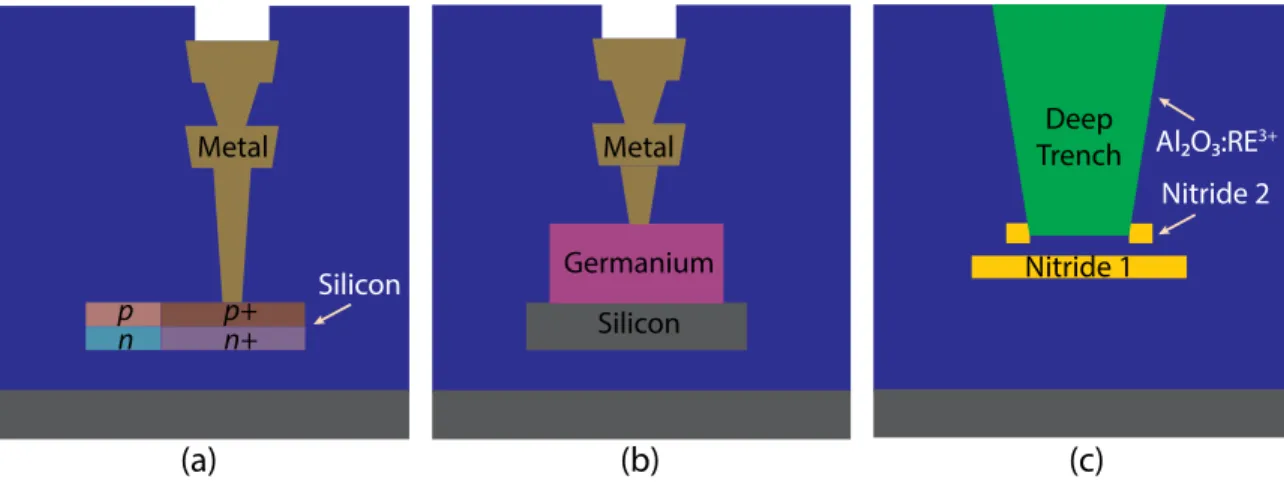
Fig. 1.1(a-c) shows three major layer stacks of the platform. We started the plat-form development with a passive silicon layer. This enables devices such as compact
p
n p+n+ Metal
Silicon Germanium
Metal TrenchDeep
Nitride 2
Nitride 1
Al2O3:RE3+
Silicon
(a) (b) (c)
Fig. 1.1: (a) Silicon layer with dopants of different types (p- or n-type) and concentrations for ap-plications such as modulators or tunable filters. (b) Germanium on silicon layer for photodetec-tion applicaphotodetec-tions. (c) Two silicon nitride layers (nitride 1 and nitride 2) with a deep trench on top for the on-chip optically pumped laser development.
vertical emitters [4], polarization beam splitters [17,18] and adiabatic microring cav-ities [19]. The highly uniform and large-scale fabrication process made it possible to have over 10,000 optical devices working together within mm×mm scale [4,20,21,22]. Though the development of passive devices enables the creation of large-scale pho-tonic circuits, applications of passive devices are limited due to lack of the ability to actively manipulate light on a chip such as data encoding through modulation and beam steering via phase control. Therefore, we introduced an active light control by incorporating doping layers into silicon, as shown in Fig. 1.1(a), to utilize its ther-mal and electric properties. With the help of the carrier plasma effect [23], both the real and imaginary part of silicon refractive index can be modulated by introducing carriers to or extracting them from silicon, enabling dynamic light modulation with ultra low power consumption [3]. In addition, the large thermal coefficient of silicon material combined with the introduction of a doping layer as a local heater makes it easier to implement efficient thermal phase shifters on chip [4, 24, 25, 26, 27]. By connecting the doping layers to upper metal layers, active devices can be individually controlled by external electrical drivers.
Although silicon is an excellent material for waveguiding, modulating and shifting on-chip light, it is not an efficient material for either light detection or light generation.
Therefore, we utilized germanium and silicon nitride that have been widely used in CMOS foundries to provide these two functions in the platform. Fig. 1.1(b) shows the layer stack of the germanium detector. Intrinsic germanium is epitaxially grown on top of the silicon, and the top part of the germanium material is doped with an n-type dopant and contacted with metals on top. By introducing a p-type dopant into the bottom silicon, a vertical p-i-n junction is formed to achieve the photodetection function.
For the laser related layer stacks (shown in Fig. 1.1(c)), we utilize a rare-earth-ion-doped glass approach to take advantage of its low noise and narrow linewidth. However, the disadvantages of this laser type are low gain per unit length and the requirement of optical pumping. The former requires a low-loss material at the signal wavelength to enable a low-loss cavity design, while the latter requires the material to be low-loss at the pump wavelength to reduce pump power attenuation. Therefore, we utilize silicon nitride as a waveguiding material for its capability to be low-loss for a broad range of wavelengths and a deep trench for rare-earth-ion-doped Al2O3
deposition outside of the CMOS foundry.
Softail 1 (2012-10-18) Softail 3 (2013-04-30) Luke (2014-12-09) Softail 6 (2015-01-21)
Luke 2 (2015-07-24) DDSP1c (2015-12-23) Luke 3 (2016-02-08) DDSP1e (2016-07-29)
Fig. 1.2: Masks taped out during my Ph.D. study.
(snap-shots of the masks are shown in Fig. 1.2, covering a variety of topics such as op-tical routing system [28, 29, 30], on-chip polarization manipulation devices [17], germanium-on-silicon detector development [31], rare-earth-ion-doped Al2O3-based
laser [11,32], wafer-scale fabrication tolerance measurement of microcavity [19], and electronics-photonics 3D integration system [14]).
5µm 10µm 5µm 10µm
10µm 10µm 5µm 2μm
(a) (b) (c) (d)
(e) (f ) (g) (h)
Tunable Filter Microdisk Modulator Photodetector Microcavity Laser
Phased Array Broadcast System Grating Coupler Phase Shifter
Fig. 1.3: A gallery of silicon photonic devices fabricated in the platform developed by MIT and SUNY Polytechnic Institute. Top-view SEMs were taken after a reactive-ion-etching (RIE) of the SiO2 cladding material. (a) A second-order tunable microring filter. (b) Two microdisk
modu-lators. (c) A waveguide-coupled Ge-on-Si photodetector. (d) The cross-section of a microcavity laser. (e) A two-dimensional phased array with a dynamic thermal tuning. (f) A microring-based optical broadcast/multicast system. (g) A grating coupler. (h) A set of cadcaded thermal phase shifters.
Based on the platform developed, we have designed and tested a wide variety of building blocks for silicon photonics. Examples of devices developed in our group at MIT are shown in Fig. 1.3, covering components such as a grating coupler, tunable filter, modulator, photodetector, microcavity laser, and system-level demonstrations such as a large-scale phased array and optical broadcast system.
While most foundry-based processes are rigid and design rules are not flexible, the platform we developed together with CNSE, SUNY Polytechnic Institute is more extensive with the capabilities such as material thickness adjustment, deep trench formation, III-V material to silicon bonding (wafer-to-wafer or metal-to-metal) and
electronics-photonics 3D integration. The flexibility of the platform not only facil-itates commercialization of silicon photonics in the communication and data-center industry, but also enables a large variety of new applications such as LIDAR, biosens-ing, and quantum computations.
1.2 Microcavities
Theories on microcavities were extensively investigated two decades ago [33]. A vari-ety of experimental demonstrations of microcavities in laser implementations [11,32], modulators [3, 6, 7], and detectors [34, 31, 35] have been achieved following the advancement in fabrication technologies. Regarding device level performance, micro-cavities can be 10 to 100 times better than non-resonant devices while maintaining a much more compact footprint. However, problems such as fabrication tolerance and process dependence [36] of microcavity designs make it hard to achieve complex photonic circuits. Therefore, robust designs of microcavities and a standardized fab-rication platform that can provide devices for various applications have become a necessity.
Input
Thr
u
Add
gap1
Dro
p
Dro
gap2
Fig. 1.4: An illustration of a waveguide-coupled microcavity used as a channel-dropping filter.
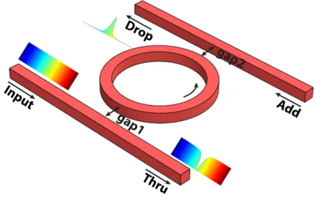
There are several advantages associated with microcavities. The first one is the wavelength-division-multiplexing compatibility by using a microcavity as a channel-dropping filter (shown in Fig. 1.4), which is a common property for resonant-based
structures. With a low-loss waveguide, data carried by the resonant wavelength/fre-quency can be selected by the microcavity and directed to drop ports of the filter with only a small amount of power loss, making it a good candidate for WDM-compatible routing systems. In Chap. 2 of this thesis, we will introduce a partial-drop filter as a new concept, which is capable of selecting only part of the input power while still maintaining the wavelength selectivity of the microcavity. With the help of partial-drop filter, further simplifications of optical multicasting networks can be achieved.
Input
Thr
u
Q
eQ
iQi = Qe ->
Full Power Absorption
Fig. 1.5: An illustration of a waveguide-coupled microcavity used as an high-efficiency absorber. Qi denotes the intrinsicQ-factor of the cavity and Qerepresents the externalQ-factor. When Qi =Qe, full power absorption can be achieved when the input wavelength matches one of the reso-nances in the cavity.
The second property is the Q-matching feature of the microcavity. As shown in Fig. 1.5, for a microcavity coupled to an external source input (e.g. in Fig. 1.5, the cavity is coupled to a bus waveguide), apart from separate resonances determined by the discrete modes within the cavity, the response of the cavity is also affected by both the loss inside the cavity (denoted as quality factor Qi) and the coupling to
the bus waveguide (indicated by quality factor Qe). When the condition Qi = Qe is
satisfied for the resonant wavelength, the microcavity will be able to trap the input light in the microcavity, providing a full absorption of the light. This concept is very useful for structures such as detectors for which a full absorption of the input power is necessary. The idea will be discussed more in Chap. 3 with both theoretical analysis
and experimental demonstrations.
P
inI
circI
circ= P
in(λ/2πn)(Q/V)
Fig. 1.6: An illustration of optical intensity enhancement using a microcavity side-coupled to a bus waveguide.
The third property of microcavity is the intensities enhancement inside the reso-nant cavity (shown in Fig. 1.6). As mentioned in Ref. [37], the circulating intensity (Icirc) in the microcavity is linked to the input power in the bus waveguide (Pin) as
I = Pin(λ/2πn)(Q/V ) (1.1)
where n is the index of the resonant mode. Therefore, even if the input power is relatively weak, the circulating intensity inside the cavity can be much higher, making it a proper platform for applications in both linear and nonlinear optics [37,38, 39]. The last one is the power consumption reduction for electrically controlled in-tegrated photonic devices such as modulators [3, 40, 7]. The switching energy for depletion-based pn-junction structures can be represented as Es = CV2 where C is
the device capacitance, and V is the required bias voltage. Therefore, the decrease in voltage with resonance enhancement and reduction in the device capacitance as a result of compactness of the microcavity will dramatically reduce the power bud-get. An example of comparing the power consumptions of a microcavity-based and Mach-Zehnder-interferometer-based modulator is included in Appendix D.
1.3 Outline of this Thesis
This thesis focuses mostly on the first three properties of microcavities while the re-duction in power consumption using a microcavity as a modulator has been rigorously investigated in Dr. Erman Timurdogan’s thesis [41].
In Chapter 2, a new concept of a microcavity-based filter – the partial-drop fil-ter is introduced. Based on the idea, a new architecture of
wavelength-division-multiplexing-compatible optical multicasting system is presented. The investigation focuses on the power uniformity, channel crosstalk, and high-speed data communica-tion operacommunica-tions of the designed system. The results presented in this chapter were published in [28, 30, 42].
In Chapter 3, a waveguide-coupled resonant germanium-on-silicon detector is pre-sented. Different aspects of the photodetector are investigated, with an emphasis on achieving high-speed operations and increasing the photo responsivities for longer wavelengths. The results presented in this chapter were submitted to Optics Letters. In Chapter4, a robust on-chip Al2O3 microcavity design and its applications in
on-chip rare-earth-ion-based lasers are presented. The analysis of the microcavity design focuses on the dependence of intrinsic Q-factors on polarization, bending radius, wavelength, and deposited film thickness. Based on the cavity design, optically-pumped ytterbium and thulium lasers are designed and investigated. Part of the results presented in this chapter was published in [32,43, 44] and the passive cavity analysis is in preparation for Optics Express.
In Chapter5, a wafer-scale analysis of adiabatic microring resonators is presented. The design is investigated using both simulation tools and large quantities of devices fabricated on a 300mm wafer. In addition, Q-factors of this type cavity under contact insertion are also analyzed and optimized with rigorous 3D finite-difference time-domain simulations, providing a new insight into using adiabatic microring resonators as a general replacement to conventional microring resonators. The results presented in this chapter were published in [19].
CHAPTER 2
Optical Routing and Multicasting Systems
In this chapter, a new architecture of a WDM-compatible optical multicasting system is presented. First, the concept of a partial-drop filter was introduced and investigated using the coupled-mode-theory. The concept was then extended to a cascaded system to achieve an optical multicasting function while maintaining a wavelength selectiv-ity. Based on the analysis, a 1-by-8 first-order microring-based multicasting system was designed and fabricated. Uniform responses and error-free data communication operations across all eight drop ports were achieved. Furthermore, to improve the roll-off speed of the filter-based structure to allow denser wavelength channel spacing for practical applications, higher-order filter-based multicast systems were studied and a 2nd-order filter-based system was demonstrated as an example.
2.1 Introduction
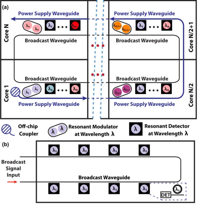
In on-chip communication networks, bus (or broadcast) topologies are among the most widely deployed, enabling all-to-all communications for rapid dissemination of instructions and data across a system. Recently, it has been proposed that wave-length selective all-to-all communications, with the transmit wavewave-length being tied to a particular core, offer a particularly compelling implementation for all-to-all on-chip networks [45]. In an integrated photonic platform, bus topologies can be implemented by cascaded power splitters [12] connected to multiprocessors. However, with simple power dividers, all wavelengths must be dropped at all sites along the network, lim-iting the potential network topologies. Importantly, a limitation of simple all-to-all topologies is that the optical power requirements scale with N2, where N is the
num-ber of sites. As a result, for large-scale implementations, limited all-to-all topologies, where the information is shared among a select group of sites are often more attrac-tive. In order to implement limited all-to-all communications networks, wavelength selective partial drops are required (see Fig. 2.1(a)) [46] with a select group of wave-lengths. The most challenging component of the all-to-all communications network is shown in Fig.2.1(b). The resonant detectors can be implemented by connecting drop ports of ring resonators to on- or off-chip detectors (DET) [inset of Fig. 2.1(b)], but are not essential for demonstrating the partial drop functionality. Thus, for the rest of the chapter, the broadcast network in Fig. 2.1(b) will be simplified to a parallel optical drop filter bank with off-chip detectors.
Previously, single large radius rings with multiple drop ports have also been utilized to act as a wavelength selective power divider [47]. However, the limited free spec-tral range (FSR) makes the approach incompatible with dense wavelength-division-multiplexed communications. To overcome these limitations, small-radius ring res-onators are preferred to enable large FSRs and broad optical bandwidths in an on-chip network.
C
or
e 1
C
o
re
N/2
C
o
re
N/2+1
C
or
e N
λN/2 λN/2 λN λN λN/2+1 λN/2+1 λN λN λN-1 λNPower Supply Waveguide
Off-chip
Coupler
λ
Resonant Detector at Wavelength
λ
λ
λ
Resonant Modulatorat Wavelengthλ
Power Supply Waveguide Power Supply Waveguide Power Supply Waveguide
Broadcast Waveguide Broadcast Waveguide
Broadcast Waveguide Broadcast Waveguide λ1 λ1 λ1 λ1 Broadcast Waveguide Broadcast Signal Input DET λ1 λ1 λ1 λ1 λ1 (a) (b)
Fig. 2.1: (a) An example approach of using wavelength selective partial drop filters in an all-to-all communications network. (b) A simplified 1-by-8 on-chip broadcast network. Inset: Implementa-tion of resonant detector at wavelengthλ1.
2.2 1st-Order Optical Multicasting System
2.2.1 Theory – Single Device
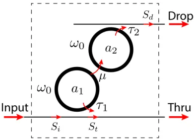
We started with the model of a 1st-order filter, shown in Fig. 2.2. It has two im-portant parameters – gap1 and gap2. For an input with a broad wavelength range, wavelengths correspond to the resonances of the cavity will be selected and guided to
the drop port, featuring a Lorentzian response shape. For a conventional filter design, gap1 and gap2 are chosen to be the same when the loss inside the cavity is negligible. This way, all the power will be guided to the drop port when the input wavelength matches one of the resonances in the cavity. However, a full power selection is not de-sired for all applications. Applications such as broadcasting or multicasting, require a partial power delivery to the drop port.
Input
Thru
Add
gap1
gap2
Drop
Dr
Fig. 2.2: A schematic of a single-ring-based filter.
(a) (b)
Full power dropped to drop port on resonance
Partial power dropped to drop port on resonance
λ0 λ0
Symmetric Gaps
Asymmetric Gaps
Fig. 2.3: 2D FDTD simulations of microring-based filters with (a) a symmetric coupling configura-tion and (b) an asymmetric coupling configuraconfigura-tion.
by setting gap1 to be different from gap2. The adjustment of gap1 and gap2 would provide a freedom to adjust the selected power level and filter bandwidth. We define this type of structure as a partial-drop filter. We first tested this idea with a 2D finite-difference time-domain (FDTD) simulation. The simulation results for both symmetric and asymmetric coupling configurations are shown in Fig. 2.3 (the colors are saturated for a better contrast). We observe that all the power on resonance is guided to the drop port for the symmetric case while only a portion of the input power is collected by the drop port for the asymmetric case. The leftover power for the latter case still stays in the bus waveguide and will continue its propagation.
Input
Thru
Drop
Add
Fig. 2.4: A coupled-mode-theory (CMT) model of a microring filter.
The phenomenon can be well explained by the coupled-mode-theory (CMT) in the time domain [48]. The model is shown in Fig. 2.4. Assuming that the internal loss of the cavity is negligible compared to the coupling strength from the waveguide, the system, therefore, can be modeled by the following equations:
dA dT = −iω0A − 2 X l=1 (A τl +r 2 τl Sl+) (2.1) Sl−= −Sl++ r 2 τl A (2.2)
The ω0 represents the cavity resonant frequency; A is the energy amplitude of the
cavity, which is normalized so that |A|2 stands for the total energy stored in the
cavity; and S is the wave amplitude, which is normalized so that |S|2 represents the power. The + and − denote the input and output to the cavity, respectively. The time constant, τ , represents the amplitude decay time constant of the cavity due to
coupling to the bus or drop waveguide. For the single input case, S2+ is zero. Since
A is the energy amplitude of the cavity, for an input frequency of ω, dA/dT = −iωA. Therefore, with simple mathematic derivations, we can achieve the thru and drop port frequency responses as
Thru = |S1− S1+ |2 = (ω0− ω)2+ (1/τ1− 1/τ2)2 (ω0− ω)2+ (1/τ1+ 1/τ2)2 (2.3) Drop = |S2− S1+ |2 = 4/(τ1τ2) (ω0− ω)2+ (1/τ1+ 1/τ2)2 (2.4)
When τ1 6= τ2 and ω = ω0, the drop port response (shown in Eqn. 2.4) gives a value
that is lower than 1 while maintaining a Lorentzian filter shape across a broadband of spectrum.
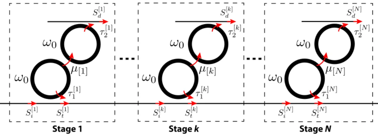
2.2.2 Theory – Cascaded System
While a standalone partial-drop filter offers partial power selection with wavelength selectivity, it cannot be treated as a termination port in a network because of the leftover power propagating in the bus waveguide. To extend the single device into a systematic design to achieve multicasting function, here we utilize a cascade-type schematic (shown in Fig. 2.5). Compared to Fig. 2.4, Fig. 2.5 adds i to represent the stage number. With the cascading effect, we have one additional constraint
S1−i = S1+i+1 (2.5)
to connect the previous stage to the current stage.
Combining Eqn. 2.3, 2.4, and 2.5, we get the following conditions to achieve a uniform power splitting into N drop ports:
τ1i+1· τi+1 2 = τ1i· τ2i (2.6) | 1 τ1i+1 + 1 τ2i+1| = | 1 τi 2 − 1 τi 1 | (2.7)
for i = 1, ...N −1. Assuming that the peak power at ω0for each port is 1/N of the total
Stage 1 Stage 2 Stage i Stage N
Fig. 2.5: A schematic of anN -stage ring-based cascaded partial-drop filter system. Each ring sup-ports a circulating mode with energy amplitudeA, incident wave amplitude S1+, transmitted wave amplitudeS1−, drop port output wave amplitudeS2−, and input wave amplitude S2+. τ denotes the amplitude decay time constant of each cavity due to the coupling to a separate waveg-uide.
where τ1
1 > τ21, we can get explicit expressions for τ1i and τ2i as
τ11 = 2[pN (N − 1) + N ]τ (2.8) τ21 = pN(N − 1) + N pN(N − 1) + N − 1/2τ (2.9) τ1i+1 = 1/2[τ1i− τi 2+ q (τi 1)2+ (τ2i)2− 6τ1iτ2i] (2.10) τ2i+1 = 1/2[τ1i− τi 2− q (τi 1)2+ (τ2i)2− 6τ1iτ2i] (2.11)
for i = 1, ...N − 1. With the constraints listed in Eqn. 2.8, 2.9, 2.10, and 2.11, all the drop port responses will be the same and can be represented by a Lorentzian frequency response function
|S i 2− Si 1+ |2 = 4/(τ 1 1τ21) (ω − ω0)2+ (1/τ )2 (2.12)
We notice that the function has a peak value of 1/N on resonance and a filter response bandwidth that depends only on the chosen τ value.
For practical design, we use dimensionless parameters such as Q-factors instead of decay time constants (τ ). The relation between Q and τ is Q = ω0τ /2. For an
eight-stage system with a total Q-factor of the first eight-stage of 2,000, the Q-factors for each stage from the theory are plotted in Fig. 2.6. We notice that the 1/N equipartition condition requires the ith stage to take 1/(N − i + 1) of the optical power that is still left in the bus waveguide. In addition, to ensure the same bandwidth at each stage,
1 2 3 4 5 6 7 8 103 104 105 Stage Number Quality Factor Q 1 Q 2 Q T Q1 Q2 Q Q = 2000 Q = 5657
Fig. 2.6: Quality factors calculated from the coupled-mode-theory to maintain an equal power dis-tribution in an eight-stage partial-drop filter bank.
Q-factors associated with the thru and drop ports must vary. This theoretical model can be easily extended to cases where the intrinsic loss of the cavity is not negligible by including a loss term τr in Eqn. 2.1 to represent the decay constant of energy in
the cavity due to intrinsic loss such as radiation, material or fabrication loss.
2.2.3 Experimental Implementation
In order to demonstrate this system on a wafer-scale fabrication platform, we also need to consider fabrication errors, wafer variations [36] and coupling induced frequency shifts (CIFS) [49] of resonant devices. Therefore, a thermal tuning mechanism needs to be incorporated into the system. For the rest of this chapter, we will utilize an adiabatic microring resonator design to add an efficient wavelength tunability to the resonators used in the system. Details of the adiabatic microring resonators design are discussed in Chap. 5.
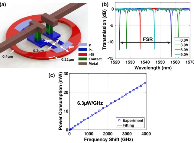
The schematic of a 3-µm-radius tunable adiabatic microring resonator is shown in Fig. 2.7(a). Integrated heaters are introduced by a p-type doping to the silicon at a concentration of 1×1018 cm−3 in the adiabatic ring waveguide, and contacts are
1520 1530 1540 1550 1560 1570 Wavelength (nm) -15 -10 -5 0 Transmission (dB) 0.0V 3.0V 6.0V 9.0V P P+ i-Si Contact Metal 1.1μm 0.2μm 0.4μm 0.22μm 1.0μm (b) (a) 0 1000 2000 3000 4000 Frequency Shift (GHz) 0 10 20 30 Power Consumption (mW) Experiment Fitting (c) FSR 6.3µW/GHz
Fig. 2.7: (a) A schematic of a tunable adiabatic microring resonator. (b) The transmission spectra of a 3µm-radius adiabatic microring resonator under different bias voltages, showing a clean free-spectra-range (FSR). (c) Power consumption of the integrated heater vs. resonant frequency shift, showing a thermal tuning efficiency of 6.3µW/GHz.
connected to the heaters by small tethers of silicon with a p+ doping at a concentra-tion of 1×1020 cm−3. The microring width is adiabatically broadened from 0.4µm to
1.1µm to minimize the loss introduced by the insertion of an integrated heater. The transmission spectra of the tunable adiabatic microring resonator under different bias voltages are shown in Fig.2.7(b), demonstrating an uncorrupted free-spectral-range of over 34nm. The tuning efficiency curve of the adiabatic microring resonator is shown in Fig. 2.7(c). We observed a tuning efficiency of 6.3µW/GHz, a little bit lower than the previous demonstration in Ref. [50]. The decrease in efficiency is mostly due to the simplification of the tether design in connection to the microcavity, resulting in a less optimized design in thermal management.
using finite-difference-time-domain (FDTD) simulations. The coefficients can then be converted to the quality factors using the following relation:
Q = 2πω0
κ2· F SR(ω) (2.13)
where κ2 represents the coupling coefficient, ω0 denotes the resonant angular
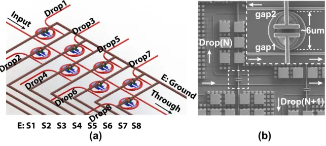
fre-quency, and F SR(ω) stands for the free-spectral-range of the resonator measured in angular frequency. (a) ~6um gap2 gap1 Drop(N) Drop(N+1)
(b)
Inp ut Thr oug h Drop1 Drop2 Drop3 Drop5 Drop7 Drop4 Drop6 Drop8 E: G round E: S1 S2 S3 S4 S5 S6 S7 S8(a)
Fig. 2.8: (a) A schematic of the optical multicast system. All the microrings shown in the figure have the same resonant frequency with different couplings to the bus and drop waveguide. (b) A scanning electron micrograph (SEM) of the fabricated device. Inset: a close-up view of the fabri-cated tunable adiabatic microring filter.
A schematic of a 1-by-8 optical multicast system is shown in Fig. 2.8(a). We fabricated the design in CNSE, SUNY Polytechnic Institute at Albany. The SEM of the fabricated device after dry etching to remove the top SiO2 cladding is shown in
Fig. 2.8(b).
For the experiment, we first took the transmission spectra of the thru port and all of the drop ports. The transmission spectra of the untuned system is shown in Fig. 2.9(a). We noticed that the resonances of all the resonators are different from each other, making it harder to tell whether the structure was correctly fabricated. In order to compensate the variations, we applied power to the integrated heaters and started aligning all the resonances to the same wavelength of 1554nm. A list
1548 1550 1552 1554 1556 1558 −40 −30 −20 −10 Wavelength (nm) Insertion Loss (dB) 1560 1580 −30 −25 −20 −15 Wavelength (nm) 1548 1550 1552 1554 1556 1558 −40 −30 −20 −10 Wavelength (nm) Insertion Loss (dB) 1553.5 1554 1554.5 −27 −26 −25 −24 −23 Wavelength (nm) Insertion Loss (dB) 92.7GHz
(c)
36.2 nm(d)
σpower= 0.11dB(a)
(b)
Port # Power (mW) Drop1 0.64 Drop2 0.36 Drop3 0.71 Drop4 0.21 Drop5 0.38 Drop6 0.13 Drop7 0.11 Drop8 0.42 Total 2.96 FSR Thru Drop1 Drop2 Drop3 Drop4 Drop5 Drop6 Drop7 Drop8 Thru Drop1 Drop2 Drop3 Drop4 Drop5 Drop6 Drop7 Drop8 Thru Drop1 Drop2 Drop3 Drop4 Drop5 Drop6 Drop7 Drop8 T ra n s m is s io n (d B m ) T ra n s m is s io n (d B m ) T ra n s m is s io n (d B m )Fig. 2.9: (a) Transmission spectra of the 1-by-8 multicasting system before thermal tuning. (b) Tuning power of each drop port. (c) Transmission spectra of the multicasting system after ther-mal tuning. Inset: spectral response of the device showing an uncorrupted 36.2nm free-spectral-range. (d) Close-up view of the transmission spectra of the multicasting system after thermal tun-ing, showing a power variation of 0.11dB on resonance with 2.96mW total tuning power.
of the tuning power for the rings of each stage is shown in Fig. 2.9(b). With the thermal tuning, the transmission spectra of those stages were aligned closely with each other (shown in Fig. 2.9(c)). The average 3dB bandwidth of the drop port responses is 92.7GHz, making this type of device capable of handling high-speed data traffic. The resulting broad range scan of the thru port is shown in the inset of the Fig. 2.9(c), showing an uncorrupted FSR of 36.2nm. The large FSR demonstrated makes it possible to allow the coexistence of more frequency channels with less mutual interference or crosstalk. A zoom-in of the top part of the transmission spectra is shown in Fig. 2.9(d), revealing a resonance variation as low as 1.7GHz and a power variation of less than 0.11dB on resonance, which are small enough to ensure equal
power distributions among all drop ports. Although in this system, eight rings and heaters are used, the total loss of the structure is only 1.1dB – no worse than that for a single fully coupled filter, a result that makes sense given that, in aggregate, the coupling of the eight-way power splitter equates to the coupling of a single fully coupled ring resonator.
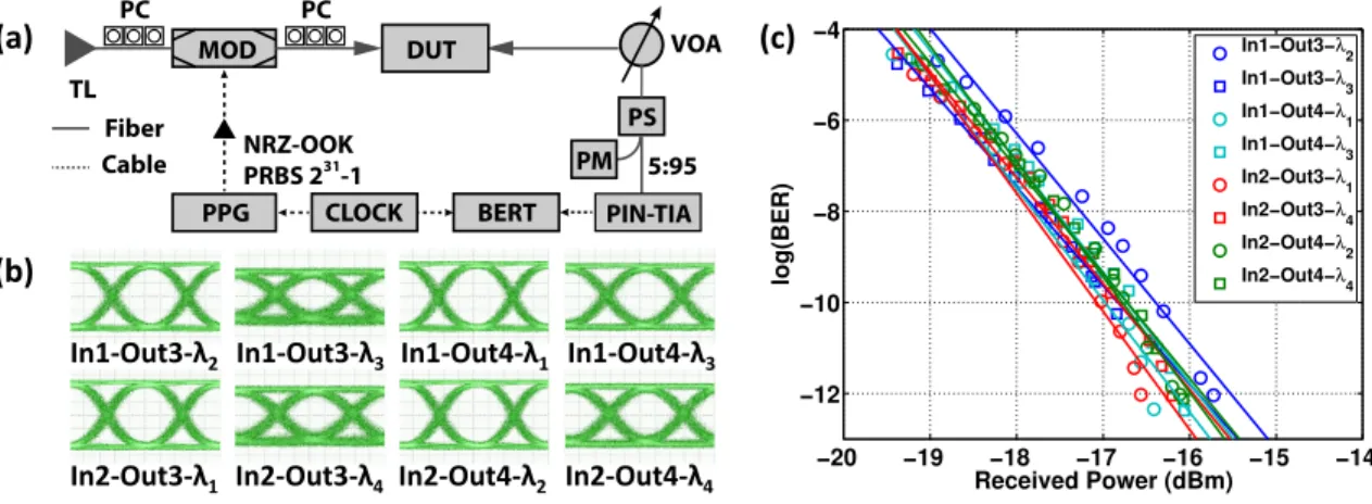
MOD PPG NRZ-OOK PRBS 231-1 PC Input Thru Drop1 Drop2 Drop3 Drop5 Drop7 Drop4 Drop6 Drop 8 E: G roun d TL PC Fiber Cable EDFA λ VOA PS 1:9 PM PIN-TIA BERT CLOCK
Drop 1 Drop 2 Drop 3 Drop 4
Drop 8 Drop 7 Drop 6 Drop 5 10Gbit/s (a) (b)
Fig. 2.10: (a) A diagram of the experimental setup for characterizing the data transmission per-formance. (b) Eye-diagrams for drop ports 1 to 8 with 10Gbit/s data rate generated from external commercial LiNbO3modulator with input laser wavelength at 1554nm.
This parallel-drop filter bank allows for high-speed data to be transmitted to all eight drop-ports with equal power distributions. A diagram of the experimental setup used to characterize the filter bank performance is depicted in Fig. 2.10(a). A continuous-wave tunable laser source (TL) was first coupled into a single mode fiber. The light was then transmitted through a commercial lithium niobate (LiNbO3)
modulator with polarization controllers (PCs) before and after the modulator to align the polarization to the transverse electric (TE) waveguide mode. In this work, the data was coded with non-return-to-zero (NRZ) on-off-keying (OOK) using a pulse
pattern generator (PPG) with a 231-1 pseudo-random bit sequence (PRBS). The
modulated light was then coupled onto the silicon chip. By thermally tuning the rings, all of the resonant frequencies were aligned to the same wavelength. For the input, the light of the tunable laser was spectrally aligned to the resonant wavelength to drop the signal to each drop port. Off-chip, the modulated optical signal was then passed through an erbium-doped fiber amplifier (EDFA), a fiber-based tunable grating filter (λ) with a 1-nm 3dB bandwidth, and a variable optical attenuator (VOA). A 1:9 power splitter (PS) was used after the VOA to direct 10% of the total power to a power meter for monitoring while transmitting the rest ( 90%) power to a high-speed (10Gbit/s) PIN photodiode and transimpedence amplifier (PIN-TIA) receiver. The signal was then evaluated using a bit-error-rate (BER) tester (BERT). Both the PPG and the BERT were synchronized to the same clock.
−13 −12 −11 −10 −9 −8 −12 −10 −8 −6 −4 Received Power (dBm) log(BER) Drop 1 Drop 2 Drop 3 Drop 4 Drop 5 Drop 6 Drop 7 Drop 8
Fig. 2.11: Experimentally measured bit-error-rate (BER) curves for the partial drop broadcast system for each drop port with a 10Gbit/s data rate generated from an external commercial LiNbO3modulator.
Fig. 2.10(b) shows the obtained eye-diagrams for all drop ports with 10Gbit/s data rate. The resulting diagrams are equally open. We then took BER curves and measured power penalties for each port using the 10Gbit/s data rate to quantify the differences between each transmission [shown in Fig. 2.11]. For each BER curve, we also verified error-free operation, achieving BERs below 10−12. The BER curves