Publisher’s version / Version de l'éditeur:
7th IEEE International Conference on Group IV Photonics (GFP), pp. 31-33,
2010-11-22
READ THESE TERMS AND CONDITIONS CAREFULLY BEFORE USING THIS WEBSITE. https://nrc-publications.canada.ca/eng/copyright
Vous avez des questions? Nous pouvons vous aider. Pour communiquer directement avec un auteur, consultez la
première page de la revue dans laquelle son article a été publié afin de trouver ses coordonnées. Si vous n’arrivez pas à les repérer, communiquez avec nous à PublicationsArchive-ArchivesPublications@nrc-cnrc.gc.ca.
Questions? Contact the NRC Publications Archive team at
PublicationsArchive-ArchivesPublications@nrc-cnrc.gc.ca. If you wish to email the authors directly, please see the first page of the publication for their contact information.
NRC Publications Archive
Archives des publications du CNRC
This publication could be one of several versions: author’s original, accepted manuscript or the publisher’s version. / La version de cette publication peut être l’une des suivantes : la version prépublication de l’auteur, la version acceptée du manuscrit ou la version de l’éditeur.
For the publisher’s version, please access the DOI link below./ Pour consulter la version de l’éditeur, utilisez le lien DOI ci-dessous.
https://doi.org/10.1109/GROUP4.2010.5643436
Access and use of this website and the material on it are subject to the Terms and Conditions set forth at
Subwavelength grating : A new type of microphotonic waveguide and
implementations to fiber-chip coupling, waveguide crossing and
refractive index engineering
Bock, Przemek J.; Cheben, Pavel; Schmid, Jens H.; Lapointe, Jean; Janz,
Siegfried; Xu, Dan-Xia; Densmore, Adam; Delâge, André; Lamontagne,
Boris; Hall, Trevor J.
https://publications-cnrc.canada.ca/fra/droits
L’accès à ce site Web et l’utilisation de son contenu sont assujettis aux conditions présentées dans le site LISEZ CES CONDITIONS ATTENTIVEMENT AVANT D’UTILISER CE SITE WEB.
NRC Publications Record / Notice d'Archives des publications de CNRC:
https://nrc-publications.canada.ca/eng/view/object/?id=1bf121f5-7c8f-4263-9674-efac04784421
https://publications-cnrc.canada.ca/fra/voir/objet/?id=1bf121f5-7c8f-4263-9674-efac04784421
Subwavelength grating:
A new type of microphotonic waveguide and
implementations to fiber-chip coupling, waveguide
crossing and refractive index engineering
Przemek J. Bock1,2, Pavel Cheben1, Jens H. Schmid1, Jean Lapointe1, Siegfried Janz1, Dan-Xia Xu1, Adam Densmore1, André Delâge1, Boris Lamontagne1, Trevor J. Hall2
1Institute for Microstructural Sciences, National Research Council Canada, Ottawa, Canada
przemek.bock@nrc.ca
2
Centre for Research in Photonics, University of Ottawa, Ottawa, Canada Abstract— We demonstrate a new microphotonic waveguide
principle based on subwavelength gratings. We also present several practical implementations of subwavelength waveguides, including a microphotonic fiber-chip coupler with a coupling loss as small as -0.3 dB, a waveguide crossover with an excess loss of 0.02dB/crossing and a PDL of <0.1 dB, and a new type of planar waveguide multiplexer.
Keywords
—
Subwavelength, grating, coupler, silicon, multiplexer, diffraction.I. SUBWAVELENGTH GRATINGS:ANEW WAVEGUIDE
PRINCIPLE
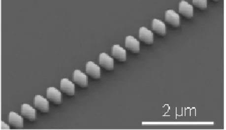
We demonstrate a new type of microphotonic waveguide based on a subwavelength grating. This is a non-resonant photonic structure (Fig. 1) formed by etching a periodic array of segments into a single crystal silicon layer of a silicon-on-insulator (SOI) wafer.
Fig. 1 Subwavelength grating waveguide fabricated in silicon-on-insulator.
In order to avoid the formation of standing waves due to Bragg scattering and the opening of a band gap near 1550 nm wavelength, the nominal structural period d is used which is less than a half of the effective wavelength λeff of the
waveguide mode. Indeed, periodic photonic lattices have been investigated to a great extent, but the efforts have almost exclusively focused on photonic crystals with d ~ λeff/2 that
have a band gap at the operational frequency range. In such
structures, a waveguide is created by introducing a line-defect in the periodic lattice that creates defect states localized within the photonic band gap created by the periodic structure. In contrast to photonic crystal waveguides, the light is confined in our SWG waveguide core by total internal reflection, as in conventional index-guided structures. The core is a composite medium formed by interlacing the silicon segments with a material of a lower refractive index which at the same time is used as the cladding material (SU-8). We fabricated the SWG waveguides in SOI wafers with 260 nm thick Si layer and a 2-µm-thick bottom oxide, using electron beam lithography in high contrast hydrogen silsesquioxane (HSQ) resist and inductively coupled plasma reactive ion etching (ICP-RIE). A 2-µm-thick SU-8 polymer layer was used as an upper cladding. The measured propagation loss of our SWG waveguide is -2.1 dB/cm for TE polarization and the PDL is mitigated (<0.5 dB) over a wavelength range of ~200 nm.
II. SWGFIBRE-CHIP COUPLER
We demonstrate the potential of subwavelength grating waveguides through the realization of practical functional components. As the first example we chose a microphotonic fibre-chip coupler, first proposed and theoretically studied in ref. [1]. The coupler principle is based on a gradual modification of the waveguide mode effective index and the corresponding mode size transformation by changing the volume fractions of the Si and SU-8 materials that form the composite waveguide core (Fig. 2). At one end of the coupler the effective mode index is matched to a 450 nm wide silicon strip waveguide for both TE- and TM-like polarizations (nTE =
2.51, nTM = 2.11), while at the end near the chip facet it is
close to that of the optical fibre (n ~ 1.5, a lensed optical fibre). The grating period is linearly chirped from 400 nm at the chip edge to 200 nm at the junction with the strip waveguide. At the same time, the waveguide width is tapered from 350 nm to 450 nm. In the first stage (Fig. 2b), near the chip edge where the mode is weakly confined, the gaps are fully opened and their lengths linearly decrease. In the second stage (Fig. 2c), near the strip waveguide where the mode is highly confined, we used silicon bridging segments to partially fill the gaps and
31
14:15 – 14:30
thereby mitigate the loss by making the transition more adiabatic. The two taper stages can also be clearly seen in the intermediate region of the coupler shown in Fig. 2d.
-30 -25 -20 -15 -10 -5 0 1430 1480 1530 1580 1630 Wavelength (nm) Lo s s ( d B ) TE TM
Fig. 2 Subwavelength grating input coupler. a) SEM image of the coupler. b) Low-confinement section near the chip edge. c) High-confinement section near the strip waveguide. d) Intermediate section. e) Transmission spectra of the insertion loss of a strip waveguide terminated at both ends with a subwavelength grating (SWG) coupler. Inset: the intrinsic coupler loss measured on a series of couplers connected back-to-back.
The TE and TM transmission spectra of the coupler are shown in Fig. 2e. The insertion loss includes the coupling loss and the propagation loss in the strip waveguide. The intrinsic coupler loss was determined in an independent measurement using a broadband Er-fibre source on a series of couplers (up to 62) connected back-to-back as -0.23 dB for TE and -0.47 dB for TM polarizations (inset of Fig. 2e). From these measurements, the total fibre-to-waveguide coupling efficiency was estimated as -0.3 dB for TE and -1.2 dB for TM polarizations. This is the highest efficiency with minimal
polarization dependence yet reported for a microphotonic coupler [2]-[4]. We also found that the coupler loss is little affected by changing the taper tip width from the nominal 350 nm to 300 nm, with an excess loss of less then 0.1 dB for both polarizations. This is improved fabrication robustness compared to other coupler designs, which also shows that the SWG waveguides are less susceptible to dimension errors arising in the fabrication process.
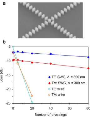
III. SWGWAVEGUIDE CROSSING
Here we demonstrate a new type of microphotonic waveguide crossing, exploiting the SWG principle. A strip waveguide is adiabatically transformed to a SWG waveguide which acts as a non-resonant mode expander in the vicinity of the crossing region, while diffraction is suppressed as a consequence of the subwavelength scale of the grating.
-25 -20 -15 -10 -5 0 20 40 60 80 Number of crossings Lo s s ( d B ) TE: SWG, Λ = 300 nm TM: SWG, Λ = 300 nm TE: w ire TM: w ire
Fig. 3 SWG waveguide crossing. a) SEM image. b) Insertion loss measured for 1×N waveguide crossings (N ranging from 0 to 80). SWG width is 300 nm, pitch 300 nm and 50% duty ratio at the crossing. Insertion loss for a direct crossing of strip waveguides is also shown (circle symbols).
The effective index of the crossing waveguides is decreased towards the intersection point by reducing the SWG duty ratio and the width of the silicon segments, as shown in Fig. 3a. Our measurements showed excellent optical isolation between the two waveguides with a crosstalk below -40 dB, more than a 25 dB improvement compared to a direct crossing of strip waveguides (260 nm × 450 nm). The crossover loss was determined on test structures with multiple (up to 80) waveguide crossings concatenated in series. The loss per crossing was estimated as -0.02 dB from the linear fit for TE polarization in Fig. 3b, and the polarization dependent loss is
-30 -15 0 0 30 60 Number of couplers Lo s s ( d B )
e
a
b
c
d
a
b
32
less then 0.01 dB. Compared to a direct crossing (circle symbols in Fig. 3b), the loss is decreased by a factor of >30. This is among the lowest loss and minimal polarization dependence yet reported for crossings in high index contrast waveguides [5]-[7]. Unlike the latter, our waveguide crossing is a binary structure and it is fabricated using a single etch step.
IV. SWGREFRACTIVE INDEX ENGINEERING IN PLANAR
WAVEGUIDES
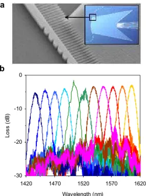
Using the SWG effect in silicon-based waveguides, media with a wide range of intermediate effective indices can be engineered by modifying the volume fractions of silicon and cladding material. This is shown on the example of an optical multiplexer circuit (Fig. 4a).
-30 -20 -10 0 1420 1470 1520 1570 1620 Wavelength (nm) L o ss ( d B )
Fig. 4 Waveguide grating spectrometer with subwavelength grating interface. a) SEM image of the subwavelength grating structure in the trench between the strip waveguide and the slab waveguide combiner. Inset: an optical micrograph of the fabricated multiplexer chip. c) Set of spectra measured at different output waveguides of the multiplexer.
We implement a subwavelength nanostructure in the trench between the strip waveguide and the slab waveguide combiner,
as shown in Fig. 4a. Near the strip waveguide an effective material index of n ~ 2.03 is created (300 nm SWG pitch, 50% duty ratio, TE polarization). Here, the trench acts as a waveguide for light diffracted by the grating towards the combiner region while at the same time as a lateral cladding for the strip waveguide. On the other side of the trench, near the slab waveguide combiner, a triangular SWG structure [8] is used as a graded-index medium to suppress Fresnel reflection for the light propagating from the trench to the slab waveguide. Transmission spectra for eleven channels of the spectrometer are presented in Fig. 4c. The achieved maximum-to-minimum transmission ratio is as large as ~20 dB while the loss is about -4 dB, allowing for wavelength filtering with a bandwidth of 170 nm. This is the largest wavelength range yet reported for a miniature spectrometer chip, for a device size of only ~160 µm × 100 µm.
V. CONCLUSION
We demonstrated a new type of microphotonic waveguide, including implementations in practical components operating at telecom wavelengths, namely a fiber-chip coupler, a waveguide crossing and an optical multiplexer. These subwavelength grating waveguides circumvent an important limitation in integrated optics, that is the fixed value of the refractive indices of the constituent materials in the absence of active tuning mechanisms.
REFERENCES
[1] P. Cheben, D.-X. Xu, S. Janz and A. Densmore, “Subwavelength waveguide grating for mode conversion and light coupling in integrated optics,” Opt. Express, vol. 14, pp. 4695-4702, 2006. [2] V. R. Almeida, R. R. Panepucci and M. Lipson, “Nanotaper for
compact mode conversion,” Opt. Lett., vol. 28, pp. 1302-1304, 2003. [3] G. A. Masanovic et al., “Dual grating-assisted directional coupling
between fibres and thin semiconductor waveguides,” IEEE Photon. Technol. Lett., vol. 15, pp. 1395-1397, 2003.
[4] D. V. Thourhout et al., “Coupling mechanisms for a heterogeneous silicon nanowire platform,” Semicond. Sci. Technol., vol. 23, pp. 1-9 2008.
[5] Y. Watanabe et al., “Broadband waveguide intersection with low crosstalk in two-dimensional photonic crystal circuits by using topology optimization,” Opt. Express, vol. 14, pp. 9502-9507, 2006. [6] W. Bogaerts, P. Dumon, D. V. Thourhout and R. Baets, “Low-loss,
low-cross-talk crossings for silicon-on-insulator nanophotonic waveguides,” Opt. Lett., vol. 32, pp. 2801-2803, 2007.
[7] P. Sanchis et al., “Highly efficient crossing structure for silicon-on-insulator waveguides,” Opt. Lett., vol. 34, pp. 2760-2762, 2009. [8] J. H. Schmid et al., “Gradient-index antireflective subwavelength
structures for planar waveguide facets,” Opt. Lett., vol. 32, pp. 1794-1796, 2007.