Automated MOSFET Parameter Extraction
by
Jerome C. Lui
Submitted to the Department of Electrical Engineering
and Computer Science in partial fulfillment of the
require-ments for the degrees of
Bachelor of Science in Electrical Science and
Engineer-ing and Master of EngineerEngineer-ing in Electrical EngineerEngineer-ing
and Computer Science
at the
MASSACHUSETTS INSTITUTE OF TECHNOLOGY
May 1995
© Jerome C. Lui, 1995. All Rights Reserved.
The author hereby grants to M.I.T. permission to
repro-duce and to distribute copies of this thesis document in
whole or in part, and to grant others the right to do so.
Author ... c
...
Department of
ctrical Engineering and Computer Science
May 26, 1995.
Certified by ...
M...L
.. ...
/~
/A
..
ofessor James E. Chung
Departinffnt of Electrical Engineering and Computer Science
\
t dThesis
Supervisor
Accepted by ... ...
;..AS;IUSrTTS
INSTI TUTEProfessork
Morgenthaler
Automated MOSFET Parameter Extraction
byJerome C. Lui
Submitted to the Department of Electrical Engineering and
Com-puter Science on
May 26, 1995
In partial fulfillment of the requirements for the degrees of
Bache-lor of Science in Electrical Science and Engineering and Master of
Engineering in Electrical Engineering and Computer Science
Abstract
The goal of this Thesis project is to set up an analysis system which will analyze the I-V
measurement data obtained from an automatic probe system which performs
measure-ments on CMOS transistors. The purpose of the analysis is to extract parameters to
char-acterize a process and provide a qualitative basis for CMOS device-design issues.
Parameters extracted in this system include: the effective channel length and width of
devices, the threshold voltage with the use of different algorithms, the subthreshold slope,
the peak transconductance, the substrate doping concentration and the flat-band voltage.
Thesis Supervisor: Professor James E. Chung
Acknowledgments
I am greatly indebted to Professor James E. Chung for providing me an opportunity to
participate in this research. Without his guidance and support this thesis would not exist.
It has been an honor and pleasure to have been supervised by Professor Chung.
I would also like to express my gratitude to Eric Chang, Rajesh Divecha, Robert Ha,
Seok-Won Kim, Wenjie Jiang, Huy Le, Daniel Maung, Beniyam Menberu, Jocelyn Nee,
Jee-Hoon Yap, and Jung Yoon. Their help and suggestions went beyond all expectations,
and have greatly contributed to this work.
I am also indebted to the following people, whose company has immensely enriched
my experience at MIT:
* To all members of my family, for their love and support throughout my life. All the members of my family have greatly sacrificed for the sake of this thesis. I hope that they will view this thesis as their achievement.
* To Esther, for being a special partner and friend for 3.5 years. You have been a great source of support, friendship, encouragement and advice. Best of luck in the future years.
* To Albert, Yuk, Andy, Bernard, Richard, Felix and Tony "Ben-Chow" Wong for being my best friends in MIT. You have been a constant source of support, friendship, advice and help during my years at MIT. Sorry for making fun on you most of the time.
* To Jocelyn, Vinci, Jenny, Vivian, Phoebe, Christina, Susan, Annie and Mary for being my best female friends in MIT. Thanks for all your care and help. Also thanks for listening to my boring words when I was in trouble.
* To King, Katherine, Sun-Man, and Leo for being my project partners for many different classes. You have made projects and classes more enjoyable.
* To WMBR for giving me a chance to be the producer of the show "Touch of Hong Kong". This is certainly a life-time experience, and I would not forget all the greatest moment in the radio station. Also thanks to the staffs of 'Touch of Hong Kong".
* To HKSS for providing many of my unforgettable activities in MIT including IM sports. Also thanks everyone in HKSS for helping me out in "Anthony Wong plus others Concert", an event of Hong Kong
Week 1992.
* To my friends overseas, especially Philip, Randy, Ceypo, Eddie, Cacin, Andrew, Angelina, Kelly, Amy, Christine and Leon, for their help and support in many different ways.
Table of Contents
1 Introduction ...7
1.1 O verview ...7
1.2 Automatic Probing System Description ...
8
2 Description of the Analysis System ... 12
2.1 NEW ANAL Program ...12
2.2 Procedure to Use the Program ...13
3 Effective Channel Length or Width ...20
3.1 Description ...20
3.2 BetaO M ethod ...21
3.3 R-measured Method ...22
3.4 Least-Squares Polynomial Approximation ...
25
3.5 Error Analysis ...
26
3.6 Implementation of Algorithm ...
27
3.7 Test and Result ...29
4 Transconductance ...
31
4.1 Transconductance Extraction ...
31
4.2 Implementation, Test and Result ...32
5 Threshold Voltage ...
34
5.1 Maximum Slope Method ...
34
5.2 Constant Current Method ...35
5.3 Mobility Degradation Method ...
37
6 Subthreshold Slope ...
40...
6.1 Subthreshold Slope Extraction ...
40
6.2 Implementation, Test and Result ...
41
7 Conclusion ...
43...
Bibliography
...
45...
List of Figures
Figure 2.1: Sample output after all the data from selected test file have been read ...14
Figure 2.2: First stage output when effective dimension calculation option is
selected. ... 15
Figure 2.3: Second stage output when effective dimension calculation option is
selected. ... 16
Figure 2.4: Sample output after the transconductance option is selected ... 17
Figure 2.5: Sample output after the threshold voltage (constant current method) option is
selected
. ...
18
Figure 2.6: Sample output after the threshold voltage (mobility degradation method) option
is selected ... 18Figure 2.7: Sample output after the subthreshold slope option is selected ...19
Figure 3.1: Measured resistance, Rmeas, versus mask level channel length, Ldrawn. ..24
List of Tables
Table 3.1: Comparison of results (Vth, Rmeas, 1/beta, Leff, and Weff) between newanal program
and iv_anal program ... 29
Table 4.1: Comparison of transconductance calculations obtained from newanal program and
iv_anal program ... 33
Table 5.1: Comparison of threshold voltage obtained from newanal program and iv_anal program
using constant current method ... 36
Table 5.2: Results of threshold voltage obtained from newanal program using three different
algo-rithm s ... 39Table 6.1: Comparison of subthreshold slope obtained from newanal program and iv_anal
pro-gram ... 41
Chapter 1
Introduction
1.1 Overview
Probing is the process of measuring current and voltage data from a device by making
electrical contact with that device using a prober. Prior to this project, manual probe
sys-tem has been used to acquire device measurement data. This was done using the
iv_mainprogram; analysis of the measurements was done using the iv_anal program. Both of
these programs are written in HT BASIC.
When probing is performed using the manual probe system, the user has to adjust the
prober manually for each device. In order to extract appropriate I-V data needed to
char-acterize the device, the user will then use the prober to step through the specified devices
with the use of the
ivmainprogram. The
iv_analprogram is used to extract useful
parameters that will characterize a process from the data acquired through iv_main
pro-gram. However, only one set of device measurements can be entered and analyzed at one
time when using the
iv_analprogram. If large amount of data is needed for statistical
study, running the
iv_analprogram can be very slow.
Last year, Robert Ha implemented a more efficient automatic probe system in his
Advanced Undergraduate project. When using the automatic prober, once the user has
defined the desired devices to be measured in the instrumentation control program, the
system will probe the transistor data automatically. This can save a lot of time in probing
when compare to the manual probe system. (More descriptions about the Automatic
Probe System will be discussed in the Section 1.2.)
This Thesis project is a continued project of Robert Ha's project. An analysis system
has been developed to analyze the measurement obtained from the automatic probe
sys-tem. This analysis system is similar to the
iv_analprogram, but it can handle a large
amount of device data efficiently. It is also able to group devices according to their die
locations and their drawn lengths or widths for analysis. Parameters such as the effective
channel length and width, the peak transconductance, the threshold voltage, the
subthresh-old slope, the flat-band voltage and the substrate concentration can be extracted from this
analysis system.
1.2 Automatic Probing System Description
This section is intended to give a brief description of the automatic probe system. For
a more detailed description, please refer to Robert Ha's report on his Advanced
Under-graduate project, "Automatic Probing on Standard Transistor Wafers".
The automatic probe system can:
* acquire transistor measurement data from the test system;
* efficiently store the measured data, and
1.2.1 Hardware Components
In order to use the system effectively, a person is assumed to have knowledge of HP
BASIC 6.0 Operating System, HP BASIC Programming Language, 4062B System
Man-ual, and the interconnections among the instruments.
The automatic probe system contains four hardware components:
1. 4062B Semiconductor Parametric Test System (SPTS)
2. R&K 1032 Prober
3. HP 9000 Series 300 Desktop Computer
4. External Hard Disks
(Both the 1032 and the 4062B are connected to the HP computer by HP-IB cables.)
An instrumentation control program called probtrans is written to control the complete
operations of the probe system. At the beginning of the program, the user has to define the
wafer type and the probe card type if the default one is not used.
1.2.2 Data Acquirement
The probtrans program is very flexible in letting the user pick devices on the wafer to
be measured. In define-wafer section, a list of DATA statements tells the program which
devices to probe. When the user wants to make a change to the devices to be measured,
these DATA statements have to be modified. The user also needs to specify the total
num-ber of devices to be measured. Future program expansion can be implemented in the
define-probe card section when several probe cards are used.
Following these sections is the main menu; here, the user can select the type of
mea-surement. The program allows 4 types of measurements:
1. Fix Vs, Vd, Vb, sweep Vg and measure Id .
3. Fix
Vs, Vd,vary
Vb, sweep Vg and measure Id .4. Fix V, Vb, vary Vg, sweep Vd and measure Id .
(where Vs=source voltage, Vd=drain voltage, Vb=substrate voltage, Vg=gate voltage, and Id=drain cur-rent.)
After the type of measurement is selected, the user is asked to specify the necessary
parameters of measurement such as the total number of steps for the sweep, source
volt-age, starting gate voltage for the sweep, ending gate voltage for the sweep, and so on. The
program will then call a subroutine to position the wafer to the desired device, and the
measurement will then be taken.
1.2.3 Data Storage
For each device, the program will create an output file to store the data in HP LIF
BDAT format. The first fifteen rows of the file is called the Header, which carries all ofthe parameters of the measurement; while the rest of the file contains the measured data.
The files are organized in a way such that the user has to input the wafer's name and
the total number of devices to be measured. For example, if the wafer's name is test and
the total number of devices to be measured are 4, then the program will create the files
testl, test2, test3 and test4. testl will store the measurements and information of the first
device indicated in the DATA statement, while test4 will store the measurements and
information of the fourth device indicated in the DATA statement.
The files will be stored in a floppy disk such that they can be transferred to a PC for
analysis. The reason that the analysis is done on the PC is because the HP is very slow.
Besides, PC's have a much larger RAM size and hard disk space as well as a faster
amount of data it has to handle.) Therefore, large amount of data can be handled easily
and sophisticated computations can be performed more time efficiently on PC's.
Since the data will be transferred to a PC environment for analysis through the floppy
disk, a manipulation has been done to minimize the memory storage space. A data point is
broken into two integers in the output file as shown below:
1.023456E-7 breaks into 1023 and -7
In this manipulation, the data is stored as an integer instead of real numbers. While
sacrificing a little in the accuracy of the data, the memory space can be reduced by a factor
of two.
1.2.4 Procedure to Use the System
The following is the procedure to use the automatic probing system:
1. Set up the prober with the probe card pins on top of die 1, device 1.
2. Place an empty floppy disk in the right hand floppy disk drive.
3. Load the probtrans program.
4. Make sure that the desired devices are listed in the DATA statements in the
define-wafer section.
5. Run the program.
6. Take the floppy disk to a PC.
7. Convert the HP LIF formatted BDAT files into DOS files by using HT Basic's
com-mand HPCOPY.
Chapter 2
Description of the Analysis
Sys-tem
2.1 NEWANAL Program
The analysis system that has been developed in this Thesis project is a program called
newanal. It provides the user with the following options:
* Input new files
* Enter extra files
* Calculation of effective channel length or width
* Peak transconductance extraction
* Threshold voltage extraction using constant current method
* Threshold voltage extraction using mobility degradation method
* Subthreshold slope extraction
Before using the program, the user has to be sure that all the files to be analyzed,
together with the newanal file, are in the same directory. The listing of the program is
included in Appendix A.
2.2 Procedure to Use the Program
Once the program has started, it will ask the user to select either the screen output or
printer output. It will also ask the user whether the devices are N-type or P-type before
reading the test files. Again, each test file consists of data probed from one device. The
main menu will then come up, and the user can exit the program anytime by pressing F8
button in the main menu.
2.2.1 Files Insertion
First of all, the user has to select "NEW FILE" to input new files by pressing the F1
button in the main menu. The program will then ask the user to enter the input wafer's
name, and the total number of tests that have been made. The user has the option of
ana-lyzing all the tests or just some selected tests. If the user chooses to analyze some selected
tests instead of all tests, then the user has to enter the tests in which he/she wants to be
analyzed by typing the test numbers of the tests.
The user can add in extra files for analysis if he/she has chosen to analyze some
selected tests at the beginning. For example, if the user has selected to analyze 5 tests out
of a total of 20 tests at the beginning, he/she can add in extra files to analyze by pressing
the F2 button in the main menu.
Every time after F1 or F2 button has been pressed, the program will read in the data
stored in the test files. After the files have been read, the measured resistance, threshold
voltage using maximum slope method, and the beta of each device will be calculated and
displayed. These parameters are needed for calculating effective channel length or width,
which in turn is needed to calculate the subthreshold slope, threshold voltage using
con-stant current method and mobility degradation method, and transconductance of each
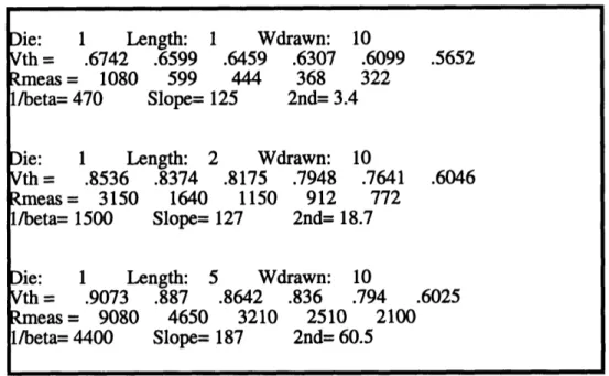
device.An example output at this stage is shown in Figure 2.1.
Figure 2.1: Sample output after all the data from selected test file have been read
2.2.2 Effective Channel Length or Width
After all the test files have been read, the user should select "L/W EFFECTIVE" to
calculate the effective channel length or width by pressing the F3 button in the main menu,
before extracting other parameters. This is because the extraction of other parameters,
such as the threshold voltage using the constant current method, requires the effective
channel dimension to be calculated. The program will then ask the user to select either
calculating effective channel length or width.
After the user has selected the appropriate option, the program will group the devices.
If the user has selected to calculate effective channel length, the program will then group
Die: 1 Length: 1 Wdrawn: 10
Vth= .6742 .6599 .6459 .6307 .6099 .5652
Rmeas = 1080
599
444
368
322
l/beta= 470
Slope= 125
2nd= 3.4
Die: 1 Length: 2 Wdrawn: 10
Vth= .8536 .8374 .8175 .7948 .7641 .6046
Rmeas = 3150
1640
1150
912
772
l/beta= 1500 Slope= 127 2nd= 18.7
Die: 1 Length: 5 Wdrawn: 10
Vth= .9073 .887 .8642 .836 .794 .6025
Rmeas = 9080
4650
3210
2510
2100
l/beta= 4400
Slope= 187
2nd= 60.5
the devices first by their die locations, and then the drawn width. If the user has selected
to calculate effective channel width, the program will then group the devices first by their
die locations, and then the drawn length.
If the user selects the effective channel length calculation, the output will display
results using the 13
0method and the R-measured method. If the user chooses effective
channel width, then only the 0 method will be used. This is because the R-measured
method is effective for calculating the effective channel length only. More details on this
will be discussed in chapter 3.
There are two stages of output no matter whether the effective channel length or width
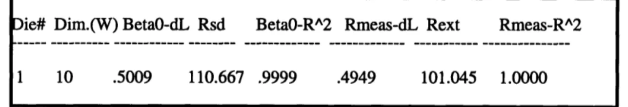
calculation is selected. The first stage of output is shown in Figure 2.2. It can be seen that
besides the delta dimension of a die, the drawn dimension and external resistance are also
shown. The coefficient of determination (r
2) is also included to indicate the correctness of
the delta dimension calculation.
r2ranges from 0 to 1, with 0 meaning the result is not
cor-rect at all, and 1 meaning the result is very reliable. Therefore, the higher the value of
r2,the more accurate is the result.
Figure 2.2: First stage output when effective dimension calculation option is selected
If the user is not satisfied with the result (i.e. having a low
r2value) of a certain group
of data, he/she can select to look at the graph by first entering the die number, and then the
drawn dimension of that group of data. According to the example in Figure 2.2, the user
will first enter 1 (for die number) and then enter 10 (for drawn dimension) if he/she wishes
ie# Dim.(W)BetaO-dL Rsd
BetaO-RA2 Rmeas-dL Rext
Rmeas-R^2
to look at the graph. After looking at the graph, the user should have an idea of where the
bad data point is, and he/she can choose to delete that data point. After deleting the bad
data point, a new calculation will be performed with the bad data point not included in the
calculation. The user also has the option of restoring all the data points after some data
points are deleted.
When the user is satisfied with the result, he/she can type a '0' to quit, and the second
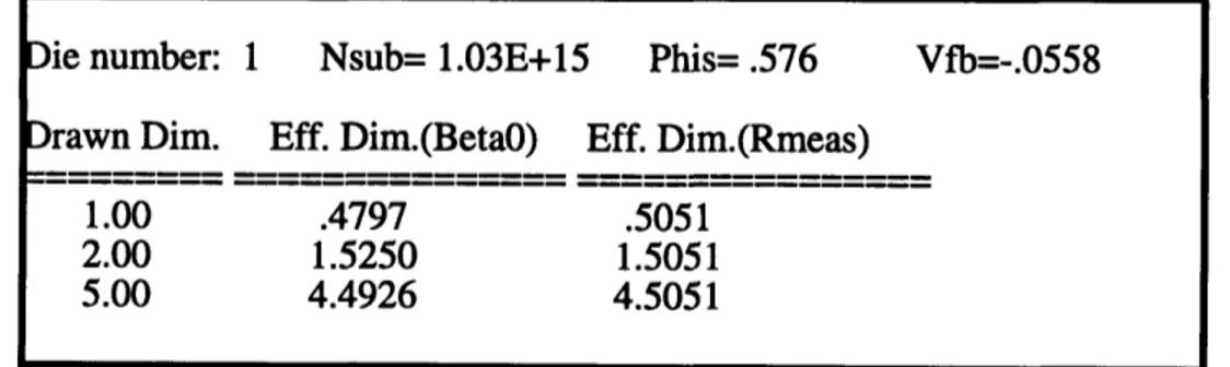
stage of output will be shown. Figure 2.3 is an example of the second stage output. As
seen in the figure, the drawn dimensions together with the effective dimensions of all the
devices are shown here. Besides the drawn and effective dimensions of devices, other die
parameters such as the substrate concentration, flat-band voltage, and phi-s are also
shown. The user also has the option of saving the result in a file of ASCII format.
ie number: 1
Nsub= 1.03E+15
Phis= .576
Vfb=-.0558
rawn Dim.
Eff. Dim.(BetaO) Eff. Dim.(Rmeas)
1.00 .4797 .5051
2.00 1.5250 1.5051
5.00
4.4926
4.5051
Figure 2.3: Second stage output when effective dimension calculation option is
selected
2.2.3 Transconductance
After the user has finished the effective channel dimension calculation, he/she can
select "TRANSCONDUCTANCE" to calculate the peak transconductances of all the
devices by pressing the F4 button in the main menu.
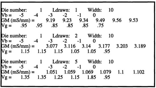
The result of output is shown in Figure 2.4, and the user can select to see the graph of
peak transconductance versus the gate voltage for each device.
Die number:
Vb=
-5
3M (mS/mm) =
Vg = .95 Die number: Vb = -53M (mS/mm) =
Vg= 1.15 Die number: Vb = -53M (mS/mm) =
Vg= 1.35 .4 .9 .4 1 .4 1 1 Ldrawn: 1 -3 -2 -1 9.19 9.23 9 t5 .85 .85 1 Ldrawn: 2 -3 -2 -13.077
3.116
.15 1.15 1.05 1 Ldrawn: 5 -3 -2 -1 1.051 1.059 .35 1.25 1.15 Width: 100
.34
9.49
9.56
.85 .75 Width: 100
3.14 3.177 3.2( 1.05 .95 Width: 100
1.069 1.079 1.1 1.85 .95 9.53 )3 3.189 1.102Figure 2.4: Sample output after the transconductance option is selected
2.2.4 Threshold voltages
The user can select "Vth: Const. I" to calculate the threshold voltages of every devices
using constant current method by pressing the F5 button in the main menu. The program
will then ask the user whether he/she wants to use the effective channel length generated
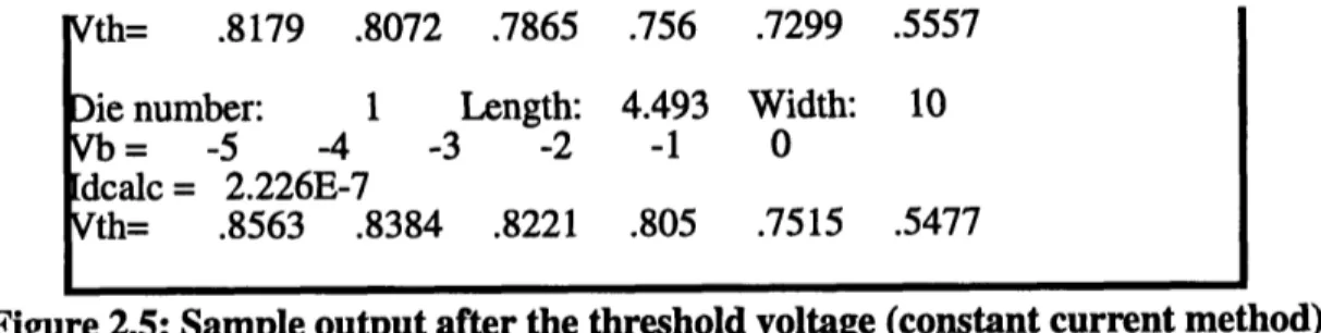
from p0 method or R-measured method in the calculation. Figure 2.5 shows an example
output of the result.
Die number: 1 Length: Vb = -5 -4 -3 -2 [dcalc = 2.085E-6
Vth= .6375 .6272 .6172 Die number: 1 Length: Vb = -5 -4 -3 -2
[dcalc = 6.557E-7
.4797 Width: .4797 -1 .6067 1.525 -1Width:
0 .5845 Width: 0 10 .5323 10Vth= .8179 .8072 .7865 Die number: 1 Length: Vb = -5 -4 -3 -2 [dcalc = 2.226E-7 Vth= .8563 .8384 .8221 .756
4.493
-1 .805.7299
Width:
0 .5557 10 .7515 .5477Figure 2.5: Sample output after the threshold voltage (constant current method)
option is selected
Similarly, the user can select "Vth: M. Degrad." to calculate the threshold voltages of
every devices using mobility degradation method by pressing F6 button in the main menu.
Since the algorithm requires the transconductance of a device to be calculated, this option
can only be selected after the transconductances of devices have been calculated. Figure
2.6 shows an example output of the result.
1 Ldrawn: -5 -4 -3 .6571 .6528 1 Ldrawn: -5 -4 -3 .8486 .8396 1 Ldrawn: -5 -4 -3 .8822 .856 1 Wdrawn: -2 -1
.5715
.5702
2 Wdrawn: -2 -1 .8273 .7667 5 Wdrawn: -2 -1.864
.8376
10 0 .568 100
.7591 10 0 .7935 .4725.6097
.6023Figure
Sample output after the threshold voltage (mobility degradation method)
2.6:
Figure 2.6: Sample output after the threshold voltage (mobility degradation method)
option is selected
2.2.5 Subthreshold slope
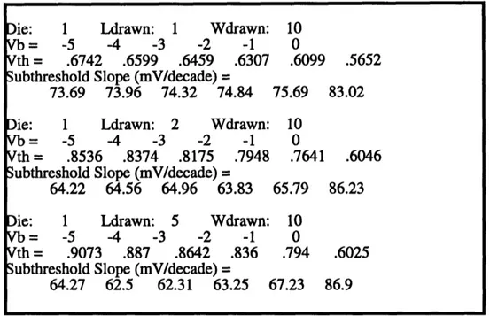
The user can select "SUBTHRES. SLOPE" to calculate the subthreshold slope of
every devices by pressing F7 button in the main menu. In calculating the subthresholdDie: Vb = Vth = Die: Vb = Vth = Die:
Vb=
Vth =slope, the user can select the set of threshold voltages calculated from either the maximum
slope method, constant slope method, or mobility degradation method to be used. An
example output is shown in Figure 2.7.
Die: 1 Ldrawn: 1 Wd
Vb = -5 -4 -3 -2 Vth = .6742 .6599 .6459
Subthreshold Slope (mV/decade) =
73.69
73.96
74.32
74
1 Ldrawn: 2 Wd rawn: -1 .6307 100
.6099 .5652.84
75.69
83.02
rawn: 10 -1 .7948 Vb = -5 -4 -3 -2 Vth = .8536 .8374 .8175Subthreshold Slope (mV/decade) =
64.22
64.56
64.96
63
Die: 1 Ldrawn: 5 Wdra);
Vb = -5 -4 -3 -2 -Vth = .9073 .887 .8642 .83
Subthreshold Slope (mV/decade) =
64.27 62.5 62.31 63.25 0 .7641 .6046 .83 65.79 86.23 wn 1 6 10 0 .794 .6025 67.23 86.9
Figure 2.7: Sample output after the subthreshold slope option is selected
Finally, after all the parameters have been extracted, the user can exit the program by
pressing F8 button in the main menu.
Die:
Chapter 3
Effective
Width
Channel
Length
3.1 Description
Technology nowadays has made submicron channel dimensions for MOS transistors
possible. However, with smaller channel dimensions (especially channel length), MOS
transistor characteristics become highly sensitive to channel dimension variations. A few
tenths-of-a-micron decrease in channel length can result in a significant decrease in
threshold voltage and a substantial reduction in source-to-drain punch-through voltage.
1Therefore, accurate channel dimension determination is essential for device analysis and
process control in MOSNLSI technology.
In the newanal program, the effective channel length is calculated by both the 0
method and the R-measured method; while the effective channel width is calculated only
by the I0
omethod. Least-squares approximation is used in implementing both of these
1. Chern, Chang, Motta, Godinho. "A New Method To Determine MOSFET Channel Length",
IEEE Electron Device Letters, Vol. Edl-1, No.9, September, 1980, p. 170.
algorithms, and an error analysis using the coefficient of determination has been
per-formed to check if the data obtained from the automatic probe system is good.
3.2 BetaO Method
This algorithm is an adaptation of the method described in the paper, "Experimental
Derivation of the Source and Drain Resistance", written by Paul I. Suciu and Ralph L.
Johnston.
The paper describes a method of extracting source-and-drain resistance from the
mea-surements of two or more transistors that are identical except for their channel lengths.
2For small drain-to-source voltage the current is approximately:
IDS = (V'cs- VT) V'DS (3.1)
where
=
0
2 (3.2)1 + UO
(VGS- VT) + U (V as- VT)
20o
= oCox
w(3.3)
eff VIGS = VG - IDSRS (3.4) V'DS = VDS- IDsRSDT (3.5)2. Suciu, Johnston. "Experimental Derivation of the Source and Drain Resistance", Transactions
where U is the mobility degradation coefficient, go is the low-field channel mobility,
Cox is the gate oxide capacitance per unit area, W is the channel width, Leff
isthe effective
channel length, Rs is the source resistance, and
RSDis the source-and-drain resistance.
3Finding the
for each
VDSby solving simultaneous equations with the use of
least-squares approximation, the delta-L can be found by plotting
Ldrawnvs 1/
0, where the
x-intercept would denote the delta-L. Similarly, by finding the P0 for each
VDSby solving
simultaneous equations stated above, the delta-W can be found by plotting
Wdrawnvs 0,
where the y-intercept would denote the delta-W
When the above relationships (equation 3.2 through equation 3.5) are substituted into
equation 3.1, the equation can be written in the form:
Io
(VGs - VT)IDS = +A(VGS -VT) VDS (3.6)
where A
U +
oRT. Then, according to Suciu and Johnston,
3(VGS - VT) 1
+
A (VGs- VT)IDSVDS E (3.7)
dE _A
U
(3.8)s
=o -
+ RD (3.8)dVGs 0 WR
By solving the above equations,
RSDcan be found.
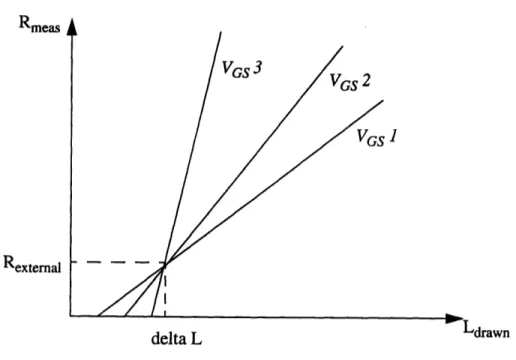
3.3 R-measured Method
The algorithm used here is followed from the method described in the paper, "A New
Method To Determine MOSFET Channel Length", written by John G.J. Chern, Peter
Chang, Richard F. Motta, and Norm Godinho.
The I-V characteristics of an MOS transistor operating in the linear region can be
expressed as: IDS = sCox VGS - VT- VDS)VDS (3.9)and
Leff Rchannel - W f V- I (3.10)RCOX Wef;
VGS-
VT- 2VDS)where
Weff = Wdrawn-AW and Leff = Ldrawn
-AL represent effective channel width
and length, respectively; AW accounts for any process bias such as print bias, etch bias,
bird's beak and lateral diffusion of channel-stop implant; AL accounts for print bias, etch
bias and lateral diffusion of source-drain dopant; and Rchannel
is the intrinsic channel
resis-tance of an MOS transistor.4A person can obtain the measured resistance, Rmeas, in the following way:
Vos
Rmeas = Ds Rexternal + Rchannel Rexternai + A (Lmask - AL) (3.11) DS
where
A = tsCOXWefJ VS
-
VDS)
(3.12)
If a set of MOS transistors with different Ldrawn'S
is prepared, then for fixed VGS, a
straight line should be obtained by plotting Rmeas versus Ldrawn while keeping A in
equa-tion 3.11 constant for all the transistors. Assuming each transistor has the same value ofRexternal, when several lines with different VGS (i.e. different A) are plotted, they would intersect at one Rexternal and AL as shown in the Figure 3.1.
The use of uniform width, Wefif transistors helps to maintain the parameter A in
equa-tion 3.12 constant. Together with least-squares approximaequa-tion, this is how effective
chan-nel length obtained from this method. However, using uniform length, Leff transistors
will not help in obtaining effective channel width. This is because A in equation 3.12 will
not be constant in this case. This is the reason why this method applies to effective
chan-nel length extraction only.Kmeas
Rexternal
UCILt L.
3.4 Least-Squares Polynomial Approximation
The least-squares polynomial approximation is a basic idea of choosing a function,
p(x), to a given function y(x) in a way which minimizes the squares of the errors. The
polynomial function should be chosen in the following form:
m
p (x) = a + ax +... + ax
(3.13)For a given set of data x
i, yi and m < N, the sum to be minimized is:
S -
Yi-ao-alxi-...-amX
i=0
(3.14)
To minimize the sum, standard techniques of calculus then lead to the normal
equa-tions, which determine the coefficients aj. For the case of a linear polynomial,
p (x) = a + alx, the normal equations are:
Soa
o+ sa
1= to
SlaO+ s2al = tl (3.15)Solving the equations yield:
s
2
t
o
- sit
ao = SOS2 5 22 S052 - $1S
ot -s t
oa, =
2 SOS2-S2SoS2
- s
(3.16)The least squares polynomial approximation for a linear polynomial function will be
used in determining the effective channel dimension for both P0 method and the
R-mea-sured method. Details will be explained in Section 3.6.
3.5 Error Analysis
To measure the correlation between variables in a linear equation, the linear
correla-tion coefficient is often used, and is given by the formula:
5, (Xi - ) (i - )
r = i (3.17)
i i
where x is the mean of the x
i's, y is the mean of the yi 's.
The value of r lies between -1 and 1. When the data points lie on a perfect straight line
with positive slope, r will take on a value of 1. The value of r holds independent of the
magnitude of the slope. If the data points lie on a perfect straight line with negative slope,
then r has a value of -1. A value of r near zero indicates that the variables x and y are
uncorrelated.
Where both x and y are assumed to be built up of simple elements of equal variability,
all of which are present in y but some of which are lacking in x, it has been proved that r
2 measures the proportion of all the elements in y which are also present in x. It can be saidthat r
2, also called the coefficient of determination, measures the percentage to which the
variance in y is determined by x, since it measures the proportion of all the elements of
variance in y which are also present in x. For example, if 2 of the elements in x
corre-2 4
spond to
-of the elements in y, then the coefficient of determination will be equal to
3 9
5. Press, Flannery, Teukolsky, Vettering. Numerical Recipes in C. Cambridge University Press,
When extracting effective channel dimension using least-squares approximation, the
coefficient of determination will be used to measure the accuracy of the data obtained
from the automatic probe system.
3.6 Implementation of Algorithm
After the test files are inserted and read by the newanal program, the program will first
calculate the threshold voltage using maximum slope method (described in section 5.1),
the measured resistance by VDS/IDS, and
using equations 3.1 and 3.2. Then, the test
files will be grouped by their die locations.After the user has selected to extract effective channel dimension in the main menu,
the program will group the test files within a die. This time, the test files will be grouped
according to their widths or lengths depend on which effective channel dimension the user
has extracted.Suppose effective channel length is selected by the user, the program will first use the
p
0method. A least-squares approximation is performed between the lengths of each
divided group of devices (with same die location and lengths) and 1/ o
0. This is because
when equation 3.3 is re-arranged:
=
A Ldrawn-A xdeltaL
(3.18)where A is the slope generated from the least-squares approximation, and deltaL is the
constant generated from the approximation divided by the slope. Then, re-arranging
equa-tion 3.18:
1
+AxdeltaL
Lf =
A
- deltaL
(3.19)
eff A
After calculating the effective channel length using 0 method, the program will then
use the R-measured method. When least-squares approximation is performed between
Ldrawn
and
Rmeasin equation 3.11, the slope will be
Aand the constant will be
Rexternal -
A x AL.
Then, when another least-squares approximation is performed
between the slope and the constant from the first least-squares approximation, i.e. between
A and Rexternal
-A x AL, the slope will be -AL and the constant will be Rexterna
.
Since
Leff
= Ldrawn
-
AL,
the effective channel length using R-measured method can therefore
be calculated by using two least-squares approximations.
When the calculations are complete, the user can select to look at the graphs of
Ldrawnvs 1/P0 (0 method) or Ldraw
nvs Rmeas (R-measured method). By looking at the graphs,
the user can detect whether there are bad data points; and if there is one, the user can select
to delete that data point from calculation. This is done by removing the device from the
group of devices and recalculating the effective channel length.
If effective channel width is selected instead of effective channel length, then
calcula-tion using only W0 method will be performed. Equacalcula-tions 3.18 and 3.19 will then be
mod-ified with 1/P0 changed to
P0,
and L's changed to W's.
After the effective channel dimension has been calculated, the program will calculate
the Nsub (substrate concentration), As, and V, (flat-band voltage) for each die. Thealgo-rithms and calculations are directly implemented from the
iv_analprogram, and the
calcu-lations are performed on the largest device within each die.
When the program has finished all the calculations, the user has the option of saving
the data to an ASCII file. The first line of the ASCII file will consist of the die number,
Nsub, s, and Vlb results. Then, from second line on, the drawn channel dimension, the
effective channel dimension using P0 method, and the effective channel length using
R-measured method (if choosing to calculate effective channel length) will be printed
respectively.
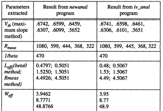
3.7 Test and Result
To test the accuracy of the calculations in the newanal program, the results from the
program are compared to the results from iv_anal program. Five devices have been
probed for testing. The results show that the calculations from newanal program are
simi-lar to those of iv_anal program:
Parameters
Result from newanal
Result from iv_anal
extracted
program
program
Vth (maxi- .6742, .6599, .6459, .6741, .6598, .6461, mum slope .6307, .6099, .5652 .6306, .6101, .5651
method)
Rmeas 1080, 599, 444, 368, 322 1080, 599, 445, 368, 322I/beta
470
470
Leff(betaO
0.4797; 0.5051
0.48; 0.5067
method; 1.5250; 1.5051 1.53; 1.5067Rmeas
4.4926; 4.5051
4.49; 4.5067
method)
Weff 3.9462 3.95 8.7771 8.7748.8766
48.9
Table 3.1: Comparison of results (Vth, Rea, I/beta, Leff, and Weff) between newanal
As seen in the table above, there are differences in some of the results between the two
programs. This is due to the fact that newanal program inputs data up to 4 significant
dig-its in integer value only, while
iv_analprogram inputs data in floating point value. This is
the place where trade-off for reducing memory spaces appears. However, since the
per-centage difference between the results is less than 1% in any cases, the result from
newa-nal program can be concluded to be very reliable.
Chapter 4
Transconductance
4.1 Transconductance Extraction
Transconductance is important since it is a measure of the activity of the transistor,
which has a direct effect on its minimum noise, driving capability and bandwidth for a
given capacitive load.
6The transconductance is given by:
dIDS
M dV.s
(4.1)If the device is operated in strong inversion, its transconductance is also proportional
to the ratio of channel width to length, the drain current, and the oxide capacitance per unit
area because an increase in any of these terms increases the output current per unit change
in gate-to-source voltage:
6. Vittoz, Eric A. "Future of Analog in the VLSI Environment", BiCMOS Integrated Circuit
GM = (IDCOXL (4.2)
However, if
WIL
is increased, GM stops increasing when the device starts operating in
weak inversion. 7 This maximum value of transconductance only depends on the drain
current:GMMAx- ID (4.3)
4.2 Implementation, Test and Result
In the newanal program, the transconductance is evaluated at every point with the
fol-lowing formula, which is a variation of equation 4.1:
G (n) =
ID n) - IDs(n - 1)(4.4)
G
M
(n) = V (n) -
VGS (n -1)
Then, for every Vd or Vb bias, the peak transconductance is determined by finding the
maximum Gm. In the program, since the transconductance is represented in mS/mm, the
above Gm is actually divided by the width of the device and scaled to get the correct unit.
A comparison between the results obtained from the newanal program and the
iv_analprogram is shown in the table below:
Transconductance (mS/
Transconductance (mS/
D(Wvra
ie0 )mm) calculated from
mm) calculated from
newanal program
iv_anal program
Ldrawn=S5m 1.051, 1.059, 1.069, 1.052, 1.06, 1.069, 1.079, 1.1, 1.102 1.079, 1.098, 1.102 Ldrawn=2gLm 3.077, 3.116, 3.14, 3.072, 3.111, 3.14,3.177,3.203, 3.189
3.177, 3.203, 3.184
Ldrawn=lm
9.19, 9.23, 9.34, 9.49,
9.185, 9.226, 9.345,
9.56, 9.53
9.485, 9.565, 9.525
Table 4.1: Comparison of transconductance calculations obtained from newanal
program and iv_anal program
The above comparison uses the result of probing three devices of the same width and
within the same die location, with six different Vb biases. It shows that the result obtained
from newanal program is very similar to the result obtained from
iv_analprogram.
The result of probing these same three devices will be used in later chapters to
com-pare other parameters extracted between newanal program and
iv_analprogram.
Chapter 5
Threshold Voltage
5.1 Maximum Slope Method
5.1.1 Theory
When deducing the threshold voltage from measurements, one useful approach is to
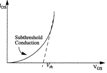
plot the drain current as a function of gate-to-source voltage, as shown in the figure below:
Subthreshold
Conduction
Figure 5.1: Extrapolation of threshold voltage using maximum slope method
The threshold voltage can be determined as the extrapolation of the portion of the
curve with maximum slope to zero current. The measured curve deviates from a straight
line at low currents because of subthreshold conduction and at high currents because of
mobility fall-off in the channel as the carriers approach scattering-limited velocity.
8(More about subthreshold conduction will be explained in the next chapter.)
5.1.2 Implementation, Test and Result
In the newanal program, the slope at each point along the
IDSvs
VGScurve is
evalu-ated for every
Vdor Vb bias. After the slope with the maximum value is found, the
thresh-old voltage is determined by:
Vth = x (n)-
y
(n) (5.1)Slopemax
where n is the point of maximum slope.
The results of Vth calculations between the two programs can be seen from table 3.1.
The results are similar with a small percentage difference.
5.2 Constant Current Method
The constant current method is another method of extracting threshold voltage. It uses
the following equation to calculate a reference current, Iref:
8. Gray, Paul & Meyer, Robert G. Analysis and Design of Analog Integrated Circuits. John Wiley & Sons, Inc. New York, 1993, p. 155.
Ief = 0.1 RA x Leff
(5.2)
If
Weff or Leffis not available, the program will
use Wdrawn or Ldrawn instead. For Leff,the user has the option of choosing the result calculated from 0o method or the
R-mea-sured method. Then, for every Vd or Vb bias, the program looks for the point where the
measured current is equal to the reference current. It will interpolate that point to get the
corresponding Vg at that value. This Vg is the threshold voltage.
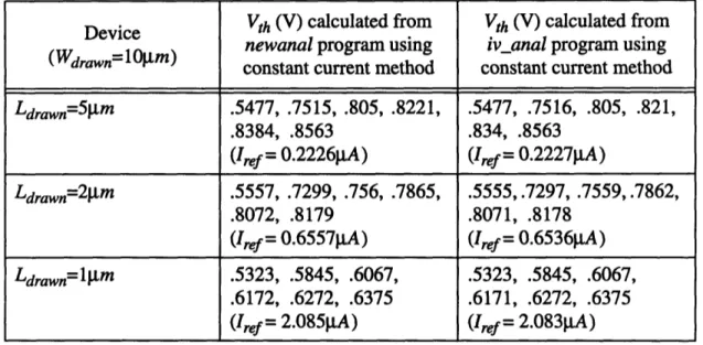
The following is the results obtained from both newanal program and
iv_analprogram
using the same three devices described in section 4.2:
Device
Vth (V) calculated from
Vth (V) calculated from
newanal program using
ivanal program using
(rawn10gm)
constant current method
constant current method
Ldrawn=5gm .5477, .7515, .805, .8221, .5477, .7516, .805, .821,.8384, .8563 .834, .8563
(Iref = 0.2226gA)
(Iref = 0.2227gA)
Ldrawn=2gm .5557, .7299, .756, .7865, .5555, .7297, .7559, .7862, .8072, .8179 .8071, .8178
(Iref = 0.6557lA)
(Iref = 0.6536gA)
Ldrawn=lgm .5323, .5845, .6067, .5323, .5845, .6067,.6172, .6272, .6375 .6171, .6272, .6375 (Iref = 2.085gA) (Iref = 2.083gA)
Table 5.1: Comparison of threshold voltage obtained from newanal program and
iv_anal
program using constant current method
Again, the results obtained from these two programs are very similar with small
per-centage of difference.
5.3 Mobility Degradation Method
5.3.1 Background
The maximum slope method will usually give good results for Vth, but it can
some-times give bad results, too. For example, a narrow P-channel device might have a very
short region where its
Idvs VGS curve is linear. That is, it can go from subthreshold to
mobility degradation very quickly. In this case, it is very difficult to pick the linear region
and extrapolate the slope accurately.
9The biggest problem with the maximum slope
method, therefore, is its total neglect of mobility degradation. This will cause
inaccura-cies in 0 which can result in large inaccurainaccura-cies in calculating effective channel
dimen-sions. It can also give incorrect values for the source-to-drain resistance.
5.3.2 Implementation, Test and Result
The mobility degradation method uses the equation:
(VGs- Vth) VDS (5.3)
d + (VGS - Vth)
and a non-linear least squares fitting algorithm is usually used to obtain ,3, Vth and 0.
However, in a typical testing environment where many dies per wafer are being tested, this
would be too slow.
10Therefore, a closed form solution would be advantageous to speed
up the calculation.9. Bendix, Peter. "Mobility Degradation Method for Obtaining Vth", The Reedholm Report, April
1994, p. 1. 10. ibid, p. 2.
To obtain a closed form solution, equation 5.3 can be re-arranged in the form:
VGs(n) -b
(n) = ax V
s
() -
(5.4)
1Vs
VDs 1where a
= D,b = V+-D-,
c = Vth-
,and n = 1, 2, 3. The solution to this
problem is demonstrated in the January, 1995 edition of The Reedholm Report, and
explicit expressions can be written for parameters a, b, and c:
111
12 (V
2- V) - 1
11
3(V
3- V) + 1
23 (V
3- V
2)
I1
(V2- V3) + 12(V3- V) -13 (V 2- V)b
II2
2V3 (V2 - V) -1113V2 (V3 - V) + I2I3 V (V3- V2) (5.6) 1112(V2 - V) - 1113(V3- V) + 1213 (V3- V2) 1I 1V(V 2- V3) +12V2 (V3- V) + 13V3(V2- V1 )c = -
(5.7)
II (V2- V3) +12 (V3- V) +13 (V2- V1)By substituting into the formulas above, Vth can be calculated as:
Vth =
b-
DS (5.8)2
Selection of the three measurement points influences the accuracy of the final solution.
According to Svoboda, two suitable points are at each side of point of maximum
transcon-ductance, and the third point is selected where influence of O is greatest, which for a 5V
process would be at gate voltage equals 5V.
1 2Since this method of extracting threshold voltage is not implemented in the iv_anal
program, the results cannot be compared. The following table includes the threshold
volt-11. Svoboda, Vladimer. "Obtaining Vth", The Reedholm Report, January, 1995, p. 2.
age extracted from the three different methods using newanal program that have been
dis-cussed in this chapter:
Vth (V), Vth (V), Mobility
Maximum
Constant
(Wdrawnl=ORlm) slope method
current method
degradation
method
Ldrawn=5 Lm .6025, .794, .5477, .7515, .6023, .7935,.836, .8642,
.805, .8221,
.8376, .864,
.887, .9073 .8384, .8563 .856, .8822 Ldrawn=2m .6046, .7641, .5557, .7299, .6097, .7591,.7948, .8175,
.756, .7865,
.7667, .8273,
.8374, .8536
.8072, .8179
.8396, .8486
Ldrawn=1 gm .5652, .6099, .5323, .5845, .4725, .568,.6307, .6459,
.6067, .6172,
.5702, .5715,
.6599, .6742 .6272, .6375 .6528, .6571Table 5.2: Results of threshold voltage obtained from newanal program using three
Chapter 6
Subthreshold Slope
6.1 Subthreshold Slope Extraction
The parameters extracted from the newanal program so far focused on the normal
region of operation where there is a well-defined conducting channel under the gate.
Changes in the gate voltage are assumed to cause changes in the channel charge only, andnot in the depletion region. However, for gate voltages less than the threshold voltage, the
applied gate potential still affects the depletion region charge and the channel charge
slightly (which is very small but not zero). The device can therefore conduct small
cur-rents for
VGS < Vth.The operation of devices in this region is called the subthreshold operation, and its
major application is for very low power applications at relatively low signal frequencies.
In the newanal program, an algorithm for extracting the subthreshold slope has been
implemented.
6.2 Implementation, Test and Result
The formula used will be:
1
Slope =
(6.1)
logId
2
- logl
VGs2-VGsl1
This is used to extract slopes at every point for the
VGSvalues below threshold. Then
for the five points right below threshold, the program looks for a set of two points whose
difference is minimum, and the average of the slope values at those two points is taken to
get the subthreshold slope. If there are less than five points to begin with, the programproceeds to take the average of all the points available. This algorithm is directly
imple-mented from the iv_anal program, but is modified such that the user can choose to use the
threshold voltage calculated from either maximum slope method, constant current method
or mobility degradation method.
The following is a table of results obtained from newanal program and iv_anal
pro-gram using the same three devices described in section 4.2:
Device
Subthreshold slope
Subthreshold slope
calculated from
calculated from iv_anal
(Wdrawnl'"10m)newanalprogram
program
Ldrawn=5RLm 64.27, 62.5, 62.31, 64.27, 62.5, 62.31, 63.25, 67.23, 86.9 63.25, 67.23, 86.9
Ldrawn=2Jtm
64.22, 64.56, 64.96,
64.22, 64.56, 64.96,
63.83, 65.79, 86.23 63.83, 65.79, 86.23
Table 6.1: Comparison of subthreshold slope obtained from newanal program and
Device
Subthreshold slope
Subthreshold slope
D(W
vice10 m)
calculated from
calculated from iv_anal
(drawn10n)
newanalprogram
program
Ldrawn=lgm
73.69, 73.96, 74.32,
73.7, 73.96, 74.32,
74.84, 75.69, 83.02
74.84, 75.69, 83.02
Table 6.1: Comparison of subthreshold slope obtained from newanal program and
Chapter 7
Conclusion
The newanal program has been successfully set up to analyze the measurements
obtained from the automatic probe system on standard CMOS transistor wafers. It can
extract MOSFET parameters such as the effective channel dimension of devices, the
threshold voltage (with the use of different algorithms), the subthreshold slope, the peak
transconductance, the substrate doping concentration and the flat-band voltage. The
results are similar to that of the
iv_analprogram with only a slight percentage difference
(less than 1% in any case). However, the newanal program can read a larger amount of
data and is able to group devices according to their die locations and drawn lengths or
widths when compared to
iv_analprogram.
In the future, more features can be added to the newanal program. One example is
wafer mapping. Since the newanal program is capable of plotting graphs, a person can
plot a graph of die number vs effective channel dimension. There is a subsection in the
program called linlin that is responsible for plotting graphs in the newanal program. With
a knowledge of HT BASIC, the code in the subsection can be easily understood, and wafer
mapping can be easily implemented.
References
Bendix, Peter. "Mobility Degradation Method for Obtaining Vth", The Reedholm Report,
April, 1994.Chern, Chang, Motta, Godinho. "A New Method To Determine MOSFET Channel
Length", IEEE Electron Device Letters, Vol. Edl-l, No.9, September, 1980.
Gray, Paul & Meyer, Robert G. Analysis and Design of Analog Integrated Circuits. John
Wiley &Sons, Inc. New york, 1993.
Ha, Robert. "Automatic Probing on Standard Transistor Wafers", M.I.T. Dept. of
E.E.C.S. Advanced Undergraduate project, May, 1994.
Press, Flannery, Teukolsky, Vettering. Numerical Recipes in C. Cambridge University
Press, New York, 1988.Suciu, Johnston. "Experimental Derivation of the Source and Drain Resistance",
Transactions on Electron Devices, Vol. Ed-27, No. 9, September, 1980.
Svoboda, Vladimer. "Obtaining Vth", The Reedholm Report, January, 1995.
Vittoz, Eric A. "Future of Analog in the VLSI Environment", BiCMOS Integrated
Appendix A
Program listing
100 190 200 YET." OPTION BASE 1 CLEAR SCREENPRINT "PLEASE NOTE THAT THIS ANALYSIS IS NOT VALID FOR MEASUREMENT #4
.t
210 PRINT "(That is: Fix Vs,Vb, vary Vg, sweep Vd and measure Id)" 220 PRINT
230 PRINT "SELECT OUTPUT OPTION:"
240 INPUT "'0' for screen output and '1' for printer & screen output",I 250 IF Pt<>0 AND Pt<>l THEN GOTO 190
260 CLEAR SCREEN
270 INPUT "N-type (0) or P-type (1) devices?",Np 271 IF Np<>0 AND Np<>l THEN GOTO 260 280 CLEAR SCREEN
310 Start: ! 320 OFF KEY
330 ON KEY 1 LABEL "NEW FILE" GOTO Newfile
340 ON KEY 2 LABEL "EXTRA DEVICE" GOTO Add_device 350 ON KEY 3 LABEL "IJW EFFECTIVE" GOTO Leff
360 ON KEY 4 LABEL "TRANSCONDUCTANCE" GOTO Trcond 370 ON KEY 5 LABEL "Vth: Const. I" GOTO Vthvd
380 ON KEY 6 LABEL "Vth: M. Degrad." GOTO Vthmd 390 ON KEY 7 LABEL "SUBTHRES. SLOPE" GOTO Subvth 400 ON KEY 8 LABEL "EXIT" GOTO Exit
405 DISP "MAIN MENU"
407 PRINT " -"
410 PRINT "(SELECT OPTIONS)" 420 GOTO 410 485 REM ********************************************************* 490 Newfile: ! 495 REM *** *** ** ************************************** 496 DIM File(520) 498 CLEAR SCREEN
500 PRINT "Please enter the input wafer's name" 510 INPUT Wafername$
520 PRINT "Please enter the number of tests made" 530 INPUT Testnumber
534 CLEAR SCREEN 535 REDIM File(Testnumber)
540 PRINT "Want to analyze all ";Testnumber;" devices?" 541 INPUT "(Type '1' if YES)",Want
560 FOR I=1 TO Testnumber 570 File(I)=I 580 NEXT I 585 Tamount=Testnumber 590 GOTO 890 600 ELSE 610 CLEAR SCREEN
620 PRINT "Among the ";Testnumber;" devices' tests, please enter the amount of tests that you want
to analyze"
630 INPUT Tamount 635 FOR I=1 TO Tamount 640 CLEAR SCREEN
650 PRINT "Enter the test number one by one" 655 PRINT "Enter '0' to re-start"
661 IF I<>1 THEN
662 PRINT "(Test numbers entered:" 663 FOR J=1 TO I-1 664 PRINT File(J) 665 NEXT J 667 PRINT")" 668 END IF 670 INPUT File(I)
675 IF File(I)=0 THEN GOTO Newfile 680 NEXT I
690 END IF
890 CLEAR SCREEN 895 DISP "PLEASE WAIT!"
901 REM ***********************************************************
902 REM This part of the program takes in the information 903 REM from the Header
904 REM *********************************************************** 920 INTEGER Head(15,2) 931 INTEGER Opt(520),Die(520),Variation(520),Num_vb(520),Num_vd(520),Num-step(520),Num_vg(520) 932 DIM Length(520),Wdrawn(520),Dmselse(520) 933 DIM Xcoord(520),Ycoord(520),Thold(520),Tdelay(520),Icomp(520) 934 DIM Vd(520),Vs(520),Vgstart(520),Vgend(520),Dms(520),Dmseffb(520),Dmseffr(520),Dmseffbw(520) 935 DIM Vb 1 (520,10),Vdstart(520),Vdend(520),Vg(520) 940 REDIM Opt(Testnumber),Die(Testnumber),Vgstart(Testnumber),Vgend(Testnumber) 950 REDIM Vd(Testnumber),Vs(Testnumber),Numstep(Testnumber),Wdrawn(Testnum-ber),Length(Testnumber) 960 REDIM Variation(Testnumber),Numvb(Testnumber),Numvd(Testnumber),Vdstart(Testnumber),Vdend(Testnumb er),Vg(Testnumber),Num_vg(Testnumber) 970 REDIM Xcoord(Testnumber),Ycoord(Testnumber),Thold(Testnumber),Tdelay(Testnum-ber),I_comp(Testnumber)
980 COM /Leastsq2/SO,S1,S2,TO,T1,Slope,Constant
990 COM /Leastsq3/
Sumxl,Sumx2,Sumxl2,Sumx22,Sumxlx2,Sumxly,Sumx2y,Sumy,Nm,Const,Linl 1,Lin2 1000 FOR Dev=l TO Tamount
1010 ASSIGN @Path TO Wafemame$&VAL$(File(Dev))
1020 ENTER @Path;Head(*)
1080 Opt(Dev)=Head(l,1) !STORES THE TYPE OF MEASUREMENT 1085 IF Opt(Dev)=4 THEN GOTO 190
1090 Die(Dev)=Head(1,2) !STORES THE DIE NUMBER
1100 Xcoord(Dev)=Head(2,1) !STORES THE X COORDINATE OF THE DEVICE 1110 Ycoord(Dev)=Head(2,2) !STORES THE Y COORDINATE OF THE DEVICE 1120 Vgstart(Dev)=Head(3,1)/1000 !STORES THE STARTING Vg
1130 Vgend(Dev)=Head(3,2)/1000 !STORES THE ENDING Vg 1140 Vd(Dev)=Head(4,1)/1000 !STORES THE DRAIN VOLTAGE 1150 Vs(Dev)=Head(4,2)/1000 !STORES THE SOURCE VOLTAGE
1160 Numstep(Dev)=Head(5,2) !STORES THE NUMBER OF STEPS OF THE MEASUREMENT 1170 Thold(Dev)=Head(6,1)/10 !STORES THE HOLD TIME OF THE MEASUREMENT
1180 Tdelay(Dev)=Head(6,2)/10 !STORES THE DELAY TIME OF THE MEASUREMENT 1190 I_comp(Dev)=Head(7,1)/1000 !STORES THE COMPLIANCE CURRENT
1191 IF Head(7,2)<>0 THEN
1192 Wdrawn(Dev)=Head(7,2) !STORES THE DEVICE WIDTH
1193 ELSE
1194 CLEAR SCREEN
1195 PRINT "Enter the W-drawn (in um) of ";Wafername$&VAL$(File(Dev)) 1196 INPUT Wdrawn(Dev)
1197 END IF
1198 IF Head(8,2)<>O THEN
1199 Length(Dev)=Head(8,2) !STORES THE DEVICE LENGTH
1200 ELSE
1201 CLEAR SCREEN
1202 PRINT "Enter the L-drawn (in um) of ";Wafername$&VAL$(File(Dev)) 1203 INPUT Length(Dev)
1204 CLEAR SCREEN 1205 DISP "PLEASE WAIT!" 1207 END IF
1208 SELECT Opt(Dev)
1210 CASE 1
1220 Vbl(Dev,l)=Head(5,1)/1000 !STORES THE SUBSTRATE VOLTAGE 1222 Num_vb(Dev)=l
1225 Variation(Dev)=l
1230 CASE 3
1240 Num_vb(Dev)=Head(8,1) !STORES THE NUMBER OF VARYING Vb 1245 Variation(Dev)=Num_vb(Dev)
1280 M=Num_vb(Dev) MODULO 2 1290 IF M--=0 THEN
1310 M=M+1 1320 K=M+9 1330 Vbl(Dev,J)=Head(K,1)/1000 1340 Vbl 1(Dev,J+1)=Head(K,2)/1000 1350 NEXTJ 1360 ELSE 1370 N=Numvb(Dev)-l 1380 Y--=0 1390 FOR J=1 TO N STEP 2 1400 Y=Y+1 1410 K=Y+9 1420 Vbl(Dev,J)=Head(K,1)/1000 1430 Vbl (Dev,J+1)=Head(K,2)/1000 1440 NEXT J
1450 Vbl(Dev,Num_vb(Dev))=Head(K+1,1)/1000 !LAST ELEMENT OF THE Vb ARRAY 1460 END IF
1470 CASE 2
1480 Vbl(Dev,l)=Head(5,1)/1000 !STORES THE SUBSTRATE VOLTAGE
1490 Num_vb(Dev)=Head(8,1) !STORES THE NUMBER OF VARYING Vb 1500 Num_vd(Dev)=Head(9,1) !STORES THE NUMBER OF VARYING Vd
1505 Variation(Dev)=Num_vd(Dev)
1510 DIM Vdl(520,10)
1515 IF Dev=1 THEN REDIM Vdl(Testnumber,Num_vb(Dev))
1520 M=Numvd(Dev) MODULO 2
1530 IF M--=0 THEN
1540 FOR J=1 TO Num_vd(Dev) STEP 2 1551 M=M+1 1560 K=M+9 1570 Vdl(Dev,J)=Head(K,1)/1000 1580 Vdl (Dev,J+1)=Head(K,2)/1000 1590 NEXTJ 1600 ELSE 1610 N=Numvd(Dev)-l 1620 Y--=0
1630 FOR J=1 TON STEP 2
1640 Y=Y+1 1650 K=Y+9
1660 Vdl(Dev,J)=Head(K,1)/1000
1670 Vdl(Dev,J+1)=Head(K,2)/1000 1680 NEXTJ
1690 Vdl(Dev,Num_vd(Dev))=Head(K+1,1)/1000 !LAST ELEMENT OF THE Vd ARRAY 1700 END IF
1710 CASE 4
1720 Vdstart(Dev)=Vgstart(Dev) 1730 Vdend(Dev)=Vgend(Dev) 1740 Vg(Dev)=Vd(Dev)
1750 Vbl(Dev,l)=Head(5,1)/1000 1760 Num_vb(Dev)=Head(8,1) 1770 Num_vd(Dev)=Head(9,1) 1780 Num_vg(Dev)=Head(9,2) 1785 Variation(Dev)=Num_ vg(Dev) 1790 M=Num_ vg(Dev) MODULO 2 1800 DIM Vgl(520,10)
1810 IF Dev=l THEN REDIM Vgl(Testnumber,Numvg(Dev)) 1820 IF M=0 THEN
1830 FOR J=1 TO Num_vg(Dev) STEP 2 1840 M=M+1 1850 K=M+9 1860 Vgl(Dev,J)=Head(K,1)/1000 1870 Vgl(Dev,J+1)=Head(K,2)/1000 1880 NEXTJ 1890 ELSE 1900 N=Numvg(Dev)-l 1910 Y=0O 1920 FOR J=1 TO N STEP 2 1930 Y=Y+1 1940 K=Y+9 1950 Vgl(Dev,J)=Head(K,1)/1000 1960 Vgl(Dev,J+1)=Head(K,2)/1000 1970 NEXTJ
1980 Vgl(Dev,Num_vg(Dev))=Head(K+1,1)/1000 !LAST ELEMENT OF THE Vg ARRAY 1990 END IF
2000 END SELECT
2010 REM ******** ***************************************** 2020 REM This part of the program stores the measured Id
2030 REM ****** ******************************************* 2040 INTEGER Arrayl(1000,2)
2050 IF Dev=l THEN REDIM Arrayl(Numstep(Dev)*Variation(Dev),2) 2060 DIM Id(520,10,100)
2070 IF Dev=l THEN REDIM Id(Testnumber,Variation(Dev),Numstep(Dev)) 2080 ENTER @Path;Arrayl(*)
2090 ASSIGN @Path TO * 2100 FOR J=1 TO Variation(Dev)
2110 Begin=J*Numstep(Dev)-Numstep(Dev)+l 2120 Finish=J*Numstep(Dev)
2130 FOR I=Begin TO Finish 2140 E=Arrayl(I,1)
2150 K=Arrayl(I,2)
2160 Id(Dev,J,I-Begin+l)=E*(EXP(2.302585093*(K-3))) 2170 NEXTI
2180 NEXT J