Circuit Techniques for Subthreshold Leakage
Reduction in a Deep Sub-Micron Process
by
Benton Highsmith Calhoun
Submitted to the Department of Electrical Engineering and Computer
Science
in partial fulfillment of the requirements for the degree of
Master of Science in Electrical Engineering
at the
MASSACHUSETTS INSTITUTE OF TECHNOLOGY
@
Massachusetts Institute
May 2002
of Technology
2002. All rights reserved.
Author ...
..
.
Department of Electrical Engineering and Computer Science
May 24, 2002
Certified by ...
...
...
Anantha P. Chandrakasan
Associate Professor
Thesis Supervisor
Accepted by ...
Chairman, Department
/11Arthur C. Smith
Committee on Graduate Students
MASSACHUSETTS INSTITUTE
OF TECKNOLOGY
JUL 3 1 2002
Circuit Techniques for Subthreshold Leakage Reduction in a
Deep Sub-Micron Process
by
Benton Highsmith Calhoun
Submitted to the Department of Electrical Engineering and Computer Science on May 24, 2002, in partial fulfillment of the
requirements for the degree of Master of Science in Electrical Engineering
Abstract
The trend of process scaling for CMOS technology has made subthreshold leakage reduction a growing concern for submicron circuit designers. Power consumption has become a principle design consideration as device sizes decrease and many more de-vices fit on a single chip. Since switching power is proportional to VfD new processes are tailored for lower supply voltages. The decrease in VDD slows down devices which requires that the threshold voltage, VT, must be lowered to maintain performance. This reduction of VT produces the exponential increase of subthreshold leakage cur-rents that has become well known.
Field Programmable Gate Arrays (FPGAs) are one type of chip that could benefit from subthreshold leakage reduction techniques. The programmable nature of FPGA designs is amenable to standby mode leakage reduction since some of the logic blocks might be unused. Leakage reduction for programmed blocks would make FPGAs more attractive to the designers of battery-operated devices.
Our research demonstrates circuit techniques to reduce subthreshold leakage for a state-of-the-art 0.13pm process. Although applicable to generic CMOS circuits in this process, the techniques in this work are specifically intended for use in low power
FPGA design.
A testchip uses Multi-Threshold CMOS (MTCMOS) style logic design to
imple-ment a new type of FPGA architecture for distributed arithmetic. The circuits are designed to provide maximum reduction in standby leakage current without degrad-ing performance of the circuits by more than 10% relative to an all low VT design. Sections of the FPGA which are not used in a given configuration are automatically placed in a low leakage state. We exhibit the new Leakage Feedback Flip-flop (LF-BFF) [1] that retains its state in standby mode. We also introduce supply voltage scaling during standby mode to reduce power consumption while retaining state. Thesis Supervisor: Anantha P. Chandrakasan
Acknowledgments
28Do you not know? Have you not heard? The LORD is the everlasting God,
the Creator of the ends of the earth. He will not grow tired or weary,
and his understanding no one can fathom.
2 9
He gives strength to the weary and increases the power of the weak.
3 0
Even youths grow tired and weary, and young men stumble and fall;
31but those who hope in the LORD
will renew their strength. They will soar on wings like eagles;
they will run and not grow weary, they will walk and not be faint.
Isaiah 40:28-31
1 0
The fear of the LORD is the beginning of wisdom, and knowledge of the Holy One
is understanding. Proverbs 9:10
I first thank my Lord Jesus Christ for graciously giving me his strength and guidance
throughout my life. I owe him everything, and I attribute all praise and glory to him.
I cannot thank Professor Anantha Chandrakasan enough for his role in this project.
Thank you, Anantha, for giving me the opportunity to join your group and to tackle this research in the first place. Your ideas, advice, and support made this work possible. I owe a lot of gratitude to Frank Honore and Theodoros Kontantakopoulos for their help on the testchip. Since Frank I and worked on the same part of the chip, his collaboration and his long hours in the lab were incredibly valuable. I surely could not have done it alone. I also thank Cypress Semiconductor for providing us with the tools to build the testchip. Alan Refalo especially gave a lot of his time and energy to support us. Thanks also to everyone else in ananthagroup for fun times and technical discussions. I especially thank Travis Simpkins for his advice and for sharing the joys and woes of chip design. I am also grateful to MARCO, Texas Instruments, and Infineon for providing funding at different points during the project.
Finally, I thank my family. My parents have supported me, as always, with their thoughts, generosity, and prayers. I especially thank my wife, Mary Kathryn. She has been so generous and wonderful for the last two years. Mare, I know I could not do this without you. Thanks to you and to Anna Grace for motivating me and for loving me so selflessly. I love you both so much.
Contents
1 Introduction and Background 17
1.1 Introduction . . . . 17
1.2 M otivation . . . . 17
1.3 Existing Techniques for Subthreshold Leakage Reduction . . . . 20
1.3.1 Switched Source Impedance . . . . 20
1.3.2 Stack Effect . . . . 21
1.3.3 Body Biasing . . . . 22
1.3.4 Dual-Threshold CMOS . . . . 22
1.3.5 MTCMOS . . . . 23
1.3.6 BGMOS and SCCMOS . . . . 24
1.4 Leakage Feedback Flip-flop . . . . 24
1.4.1 MTCMOS Sequential Circuits . . . . 24
1.4.2 Leakage Feedback Gate . . . . 25
1.4.3 LFBFF Design . . . . 27
1.5 Contributions of Thesis . . . . 28
2 Characterizing Leakage in a State-of-the-Art 0.13pm CMOS Process 29 2.1 Introduction . . . . 29
2.2 Leakage Models . . . . 29
2.3 Subthreshold Current Versus VGS . . . . . . . . . 30
2.3.1 Subthreshold Slope . . . . 31
2.4 VDS and the DIBL Coefficient . . . . 34
2.6 Subthreshold Leakage Versus Device Size . . . . 3 Voltage Scaling During Standby Mode
3.1 Introduction . . . .
3.2 Voltage Scaling Concept . . . . 3.3 Varying Supply Voltage and the LFBFF . . . .
3.3.1 Storing a Logic '1' . . . . .. 3.3.2 Storing a Logic '0' . . . .. 3.3.3 Power Savings Using Voltage Scaling . . . . 3.3.4 Levels of Standby . . . . 3.4 Adaptively Scaling Supply Voltage . . . .
3.4.1 Architecture for Adaptive Flip-Flop Voltage Scaling . . . . 3.4.2 Designing Flip-Flops for Failure . . . . 3.4.3 Effect of Variation on Flip-Flops . . . . 4 Testchip Design and Architecture
4.1 Introduction . . . . 4.2 Subthreshold Leakage and FPGAs . . . . 4.3 Test Chip Circuits . . . . 4.3.1 Top Level Design . . . . 4.3.2 C ore . . . . 4.3.3 Data Registers . . . .
4.3.4 Peripheral Components . . . .
5 Testchip Implementation
5.1 Introduction . . . .
5.2 Multiple Power Regions . . . . 5.3 Sleep Mode Specifics . . . .
5.3.1 Multiple Regions for Sleep in a CLB
5.3.2 Fine Granularity . . . .
5.3.3 Sizing Sleep Devices . . . .
37 41 41 41 42 43 47 52 53 55 55 56 58 63 63 63 64 65 65 72 73 79 79 79 81 81 87 88
5.3.4 Sleep, FFs, and Clock . . . .
5.3.5 Energy Overhead for Sleep Mode . . . . 5.4 Stopping Sneak Leakage Paths . . . . 5.4.1 Causes of Sneak Leakage Paths . . . . 5.4.2 Sneak Leakage Paths Eliminated from the Testchip 5.4.3 Guidelines for Preventing Sneak Leakage Paths .
5.5 Layout . . . . 5.5.1 General Strategy . . . .
5.5.2 Clock Signals . . . .
5.5.3 Power Signals . . . . 5.5.4 Critical Path Implementation . . . ..
5.5.5 Layout Screenshots . . . .. 6 Conclusion
6.1 Introduction . . . .
6.2 Summary and Results . . . .
6.2.1 Flip-Flop Voltage Scaling . . . . 6.2.2 Low Power FPGA Testchip . . . . 6.2.3 CLB Power Savings Using Voltage Scaling...
6.3 Contributions . . . . 6.4 Future W ork . . . . 6.4.1 Voltage Scaling . . . . 6.4.2 Low Power FPGA Testchip . . . .
88 89 92 93 94 101 102 102 103 104 104 106 109 109 109 109 110 112 113 114 114 114
List of Figures
1-1 Sub-threshold (SD) Leakage
1-2 Trend of Increasing Leakage Power . . . . 1-3 Leakage Power for Future Chips . . . . 1-4 Switched-Source-Impedence . . . . 1-5 Artificial Creation of Stack Effect . . . . . 1-6 MTCMOS Schematic . . . . 1-7 MTCMOS Balloon Flip-Flop . . . . 1-8 Leakage Feedback Gate . . . . 1-9 Leakage Feedback Flip-Flop . . . .
2-1 Subthreshold Current vs VGS . . . .
2-2 Model versus Simulation for Varying VGS
-2-3 Simulation of Subthreshold Leakage versus 2-4 Model Versus Simulation for Varying VDS . 2-5 2-6 2-7 2-8 3-1 3-2 3-3 3-4 3-5 VDS
Simulation of Subthreshold Leakage versus Temperature
Model Versus Simulation for Varying Temperature . . . .
Threshold Voltage Variation with Device Size . . . . Threshold Voltage Variation with Device Size . . . . LFBFF in Sleep Mode . . . .
LFBFF Holding a '1' . . . ..
Output Node Changing Value for Stored '1' .
Internal Node Changing Value for Stored '1' .
LFBFF Storing '1' at VDD =80mV . . . . 18 . . . . 19 . . . . 19 . . . . 20 . . . . 22 . . . . 23 . . . . 25 . . . . 26 . . . . 27 31 32 34 35 36 36 37 38 . . . . 42 . . . . 44 . . . . 45 . . . . 46 . . . . 47
-3-6 LFBFF Holding a '0' ...
3-7 High VT Inverter Output for Varying Widths . . . . 3-8 Output Node Changing Value for Stored '0' .. . . 3-9 Internal Node Changing Value for Stored '0' .
3-10 LFBFF Storing '0' at VDD =80mV . . . . 3-11 Power Reduction from Voltage Scaling . . . . 3-12 Power Reduction Factor from Voltage Scaling . . . 3-13 Adjustable Voltage Scaling Architecture . . . .
3-14 LFBFF Storing '1': Sized to Fail at 130mV . . . . .
3-15 LFBFF Storing '0': Sized to Fail at 130mV . . . . . 3-16 Effect of Temperature on FF Failure . . . . 3-17 Effect of Process Corners on FF Failure . . . .
4-1 Test Chip Setup . . . . 4-2 Configurable Logic Block Used on the Test Chip . . 4-3 Slice Diagram . . . . 4-4 Programmable Transmission Gate for Interconnect . 4-5 Top Level Switching Diagram . . . . 4-6 Slices Implementing an 8-tap, 16-bit FIR Filter . . 4-7 Data Register Diagram . . . . 4-8 Input Generation Hardware and Operation . . . . . 4-9 Timing Diagram for the Capturing Filter Output 4-10 Clock Gating System . . . .
5-1 Sleep Regions within the CLB . . . .
5-2 Sleep Signal Selection for LUT . . . .
5-3
5-4
5-5 5-6 5-7
Short Circuit Current due to Poor Sleep Region Inte Steady-State Current Change Entering Sleep . . . .
Clock Buffers to Flip-Flops During Sleep Mode . .
CLB Current and Energy Transitioning to/from Sle Break-Even Time for Entering Sleep Mode . . . . .
. . . . . . . . 48 . . . . 48 . . . . 50 . . . . 50 . . . . 51 . . . . 52 . . . . 53 . . . . 55 . . . . 57 . . . . 58 . . . . 59 . . . . 60 . . . . 65 . . . . 66 . . . . 68 . . . . 68 . . . . 70 . . . . 71 . . . . 72 . . . . 74 . . . . 76 . . . . 76 . . . . 82 . . . . 82 rface . . . . 84 . . . . 86 . . . . 89 ep Mode ... 90 . . . . 91
5-8 5-9 5-10 5-11 5-12 5-13 5-14 5-15 5-16 5-17 5-18 5-19 5-20
Effect of Sneak Leakage Paths on Current Reduction .
High VT Latch Used in LUTs . . . . Sneak Leakage Paths in 16-bit LUT . . . . Final Design for 16-bit LUT . . . . Sneak Leakage Path through Multiplexor . . . . Sneak Leakage Path Eliminated through Multiplexor . Sneak Leakage Path Due to Missing Sleep Device . . .
Subtle Sneak Leakage Path Due to Shared Sleep FETs Isolating LFBFF Input Removes Sneak Path . . . . Layout Placement for a Slice (with 4 CLBs) . . . . Layout of Full Adder . . . . Layout of CLB . . . . Layout of Chip . . . .
6-1 Leakage Current Reduction Entering Sleep . . . . 111
. . . . 93 . . . . 94 . . . . 94 . . . . 96 . . . . 97 . . . . 97 . . . . 98 . . . . 99 . . . . 100 . . . . 105 . . . . 106 . . . . 107 . . . 108
List of Tables
LFBFF State for Stored '1' . . . . ..
LFBFF State for Stored '0' . . . . Possible Set of Standby States . . . . Signals Multiplexed by Configuration Bits Mapping of Slice Signals to Buses . . . . . Shift Registers on the Testchip . . . . Power Supply Regions...
Configuration Bit Constraints Steady-State Current Reduction
6.1 Breakdown of CLB Power . . . . 43 . . . . 47 . . . . 54 67 69 73 80 85 85
Using Sleep Regions
. . . 111 3.1 3.2 3.3 4.1 4.2 4.3 5.1 5.2 5.3
Chapter 1
Introduction and Background
1.1
Introduction
This chapter motivates the need for subthreshold leakage reduction techniques and discusses existing methods for providing such reduction.
1.2
Motivation
The trend of process scaling for CMOS technology has made subthreshold leakage reduction a growing concern for submicron circuit designers. Power consumption has become a principle design consideration as device sizes decrease and many more devices fit on a single chip. Since switching power is proportional to CL VJD new
processes are tailored for lower supply voltages. Since the decrease in VDD slows down logic gates, the threshold voltage, VT, must be lowered to maintain performance. This reduction of VT produces the problematic increase of subthreshold leakage currents according to the well-known equation
where I, = poC V2 e 18. This equation can be approximated in the equally
well-known form
Ileak 0 W10 s(1.2)
wo
where S = nVth in 10. As these equations show, leakage currents increase exponen-tially as VT scales down with technology.
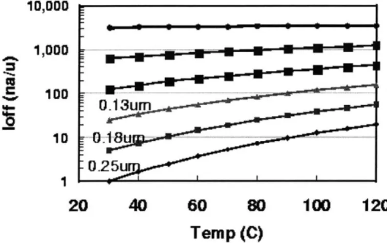
10,000 1,000 ca 0.13um '4-00 0.25u 20 40 60 80 100 120 Temp (C)
Figure 1-1: Sub-threshold (SD) Leakage
The graph in Figure 1-1 shows how subthreshold leakage scales with technology[2]. The figure shows that subthreshold leakage has increased by about 5X per generation for the last three generations. The numbers in the plot are normalized to lnA/pm for the 0.25pm technology at room temperature. Clearly, this trend could cause extremely high subthreshold currents for future technologies.
In fact, Figure 1-2 shows research from Intel that predicts leakage power consuming over half of a chip's power at operating temperatures in a deep submicron process. Intel also shows in Figure 1-3 how the increase in Ioff will produce exponential rises in leakage power for digital chips in future technologies. These plots from Intel give a representative picture of the concern about leakage current trends across the industry. If unaddressed, this leakage power will exist in both active and standby modes. Although some new techniques address active mode leakage reduction, most tech-niques target standby leakage reduction. Many low power devices operate primarily
90 0. L, 15mm die, 0.7V a 8 Leakage 8 0 -E d e ....- ...-- .. ...- -... .4 9 % 70 41% 60 33% -150 % 14%/9% w40 -o 30 20 - - - -10 Temp (C)
Figure 1-2: Trend of Increasing Leakage Power
in bursts of activity amid significant periods of inactivity. Standby leakage reduction techniques can reduce the power dissipation of such devices during these standby periods. 1,000 m 30 M Total transistor I V 09 100 .15mm Die 12 Temp=100C 1.5V S 10 2V 0 0
025u 0.18u 0.13u 90nm 65nm 45nm
1.3
Existing Techniques for Subthreshold Leakage
Reduction
Equation 1.2 shows that exponential decreases in 'leak are possible by either increasing
the threshold voltage or by decreasing VGS. Existing techniques explore both of these options.
1.3.1
Switched Source Impedance
One obvious method for reducing leakage current is to decrease VGS in standby mode
by raising the source voltage through switched-source-impedence CMOS [3]. In this
approach, a passive resistor is switched in between a gate's source nodes and ground during standby mode. During active mode, the resistor is shorted out so that there is no additional delay penalty.
In Out (0 in sleep) Vx Rbig Sslp log ID Current Savings -Vx Vt=Vtl - - Vt=Vt2 - Vgs Vgs=0
(a) Circuit Example (b) Savings
Figure 1-4: Switched-Source-Impedence
The presence of the resistor in standby mode introduces a positive voltage at Vx due to the leakage current through RBIG (see Figure 1-4(a)). The voltage Vx reduces
causes an increase in the threshold voltage due to the well-known equation:
VT = Vto + ( VSB + 2qF - 2OF)
This higher VT causes a shift in the current-VGS curve in Figure 1-4(b) from VT VT1
to VT = VT2. Furthermore, the increased Vx reduces VGS of the NMOS device, causing the operating point to shift downward along the current-VGS curve. The combination of these two effects lowers the standby leakage current. In practice, switched-source-impedence circuits are rare because the resistor must be large and resistor placement depends on knowing the standby state of every gate. Since there is no perfect switch, the resistance of the switch often replaces the explicit resistor for this technique.
1.3.2
Stack Effect
A similar and more practical technique for subthreshold leakage reduction takes
ad-vantage of the stack effect. The term stack effect refers to the reduction of subthresh-old leakage by stacking multiple FETs in series. Figure 1-5 shows a case of artificially introducing the stack effect to an inverter, but stacks of transistors occur naturally in many logic gates (i.e. - NAND). The stack effect provides leakage reduction in
the same way as switched-source-impedence. The last device in the stack essentially appears as an impedence to any leakage current, so the voltage Vx becomes non-zero. At that point, the effects shown in Figure 1-4(b) occur as previously described. Notice that the imposed stack effect approach is essentially the switched-source-impedence approach without the resistor. This approach just uses the resistance of the non-ideal switching FET in an off state.
Designers take advantage of the stack effect in two ways. First, one can exploit natural stacks in a circuit by determining an input vector at design time that turns off stacks of devices. Several algorithms exist for applying test vectors to a circuit at design time to find the vector that generates the lowest leakage current (e.g. - [4]
[5]). When the circuit enters standby mode, this low-leakage vector is muxed into the
In Out In Out
w (0 in W/2
Vx
W/2
Figure 1-5: Artificial Creation of Stack Effect
Artificial introduction of stacks to a circuit [6] can enhance the gains from the vector-finding method of leakage reduction. In this approach, stacks are introduced to gates off of the critical path (Figure 1-5). While slower itself, the new gate presents the same capacitive load at its input, so it does not slow down previous gates. This method trades off speed on non-critical paths and design time for reduced leakage. A new model for determining the savings introduced by forcing stacks allows designers to determine the usefulness of the approach for a given technology [6].
1.3.3
Body Biasing
A entirely different approach to reducing subthreshold leakage biases the body voltage
to change VT. There are many angles taken to use this technique, but they all require isolation of the bulk for different FETs (as in a triple well process). This research will not focus on body biasing.
1.3.4
Dual-Threshold CMOS
Dual-threshold CMOS techniques use FETs having two thresholds to reduce leakage currents. The most straightforward application of dual-threshold CMOS uses all low
VT FETs on the critical path and high VT FETs off of the critical path. The high VT devices placed at design time reduce leakage while increasing delay off of the
critical path. The placement of these devices can become complicated since the high
Nevertheless, several algorithms exist for that purpose (eg - [7]). One advantage of
dual-threshold CMOS is that the leakage savings occur in both active and standby modes. Disadvantages include more complicated design time and the inability to stop critical path leakage during standby mode.
Dual-threshold CMOS is particularly useful for some special logic styles. For example, domino logic can use high VT devices on the precharge path [8]. All of the pull-down paths remain fast because of the low VT devices, but each path between the rails contains at least one high VT device. This allows the tradeoff of precharge time with reduced leakage.
1.3.5 MTCMOS
Multi-Threshold CMOS (MTCMOS) refers to a circuit technique that uses a high
VT footer and/or header FET to sever a circuit from the power rails (Figure 1-6) [9].
Similar approaches have been applied to caches [10, 11] and to DRAMs [12]. In active
Sleep - Chigh VT
Inputs r wVL T _. Outputs
Sleep
Ad
,high VTFigure 1-6: MTCMOS Schematic
mode, the high VT switches are on to enable regular circuit operation. Turning off the high VT devices in standby mode places at least one high VT FET on each path
from power to ground, thereby reducing the leakage current significantly.
Sizing the sleep devices is no easy task. Small sleep devices further reduce the leakage current in standby mode but slow down transitions in active mode. The loss of performance occurs because smaller sleep devices sink less current through to ground.
This exacerbates the bouncing created at the virtual rails and effectively pinches VDS
for the low VT circuit. Furthermore, this rail bounce depends on the discharge pattern of the circuit, so it can be difficult to predict worst-case performance.
Combinational logic blocks only need a sleep device on one rail, but sequential MTCMOS circuits are more complicated. Simply disconnecting a circuit from the rails in standby destroys any state previously stored in that circuit. Special care is necessary to retain state in MTCMOS sequential circuits.
Despite some of the design difficulties, MTCMOS techniques appear to be viable for reducing leakage currents in new technologies.
1.3.6
BGMOS and SCCMOS
Two additional proposals for reducing leakage basically increase the effectiveness of MTCMOS sleep transistors. The Boosted Gate MOS (BGMOS) approach [13] sug-gests that overdriving the gate voltage of sleep devices in active mode can reduce the area devoted to sleep devices. The overdriven (above VDD) gate voltage enables a smaller device to sink the required amount of current in active mode while still effectively stemming the leakage current in standby mode. A similar approach called Super Cut-off CMOS (SCCMOS) advocates underdriving gate voltages in standby mode [14]. For example, an NMOS sleep device would be turned off in standby mode with a negative gate voltage rather than a gate voltage of 0 volts. From equation 1.2 we see that the negative gate voltage provides exponentially decreasing leakage current through the sleep device.
1.4
Leakage Feedback Flip-flop
1.4.1
MTCMOS Sequential Circuits
Straightforward MTCMOS design prevents the use of sequential logic because it dis-connects internal nodes from the power rails. Without an active source to hold a stored value, any sequential gate could lose its state due to floating nodes.
Several strategies exist for implementing sequential circuits using the MTCMOS approach. For example, high VT devices placed in parallel with low VT devices can hold the state of storage nodes while the low VT inverters are disconnected from the rails[9]. This approach adds the additional capacitive load of the high VT device on the critical path of the flip-flop. A high VT "balloon" circuit consisting of back to
B2 B1 C
C 5~2
Figure 1-7: MTCMOS Balloon Flip-Flop
back inverters can hold state at a given node [15, 16, 17]. Figure 1-7 shows one design using the balloon circuit. All of the low VT inverters in the figure have implicit high
VT sleep devices at both rails. This approach increases the load on the critical path. It also can require complicated timing to store the data into the balloon and to retrieve data from the balloon. Another approach uses the output of a flip-flop to control the sleep state of the device conditionally [18]. This permits one rail to drive the output actively while conditionally disconnecting the output node from the other rail. This implementation cannot retain state correctly if the inputs to the flip-flop change.
This project focuses on the Leakage Feedback Flip-flop (LFBFF) proposed in [1]. The next two sections describe this flip-flop in more detail.
1.4.2
Leakage Feedback Gate
A leakage feedback gate holds its state during standby mode by maintaining an active
path to one rail contigent on the output. Figure 1-8 shows the concept at work. When the gate enters sleep, devices M1 and M3 turn off. One of either M2 or M4 also turns
Sleep M 2
in out
___ M4
Sleep
M3---Figure 1-8: Leakage Feedback Gate
off depending on the output of the gate at the time that the sleep signal rises. For example, suppose that out is '1' when sleep is asserted. This means that the gates of M2 and M4 are '0', so M4 is off and M2 remains on. After the sleep signal turns off devices MI and M3, the output node connects actively to the VDD rail through M2. The turned-off pair of M3 and M4 disconnect the output node from ground, effectively gating all subthreshold leakage paths with high VT devices. The opposite
occurs when out is '0'.
This gate has the interesting property of maintaining its output even when the input node floats. Take the case of the example above. When the gate enters sleep, node in is '0'. Suppose that in floats to an intermediate value or even to '1' once in
sleep. The feedback path at the output continues to keep M2 on and M4 off. Node
in changing causes the NMOS inside the inverter to turn on and the PMOS in the
inverter to turn off. Now, the low VT PMOS device in the inverter buffers the output
node from VDD, but the high VT devices M3 and M4 buffer it from ground. The order
of magnitude higher leakage current through the low VT device will continue to hold
the output at the correct logical value of '1'. The opposite occurs if the output was originally '0'.
Even though mismatched leakage currents can hold the output at the correct volt-age when the inputs float, the lack of any active connection at the output node makes it particularly susceptible to capacitive coupling. A strong coupling with a nearby
node that switches could overcome the mismatch in leakage currents to produce an incorrect value at the output. Designers must position leakage feedback gates (and flip-flops) to prevent such capacitive coupling. Strong capacitive coupling often is eliminated inherently because the leakage feedback gate (or flip-flop) lies in the midst of an entire region of devices in sleep state. This means the surrounding devices will not be switching as long as the region remains in standby mode.
The properties of the leakage feedback gate make it useful for sequential logic design. The gate also can provide an interface between MTCMOS and CMOS gates. The floating nodes generated in the MTCMOS region during sleep mode do not affect the state of the LFB gate. Thus, it maintains an actively driven input to the CMOS logic even when the MTCMOS circuits are in standby mode.
1.4.3
LFBFF Design
A leakage feedback flip-flop (LFBFF) [1, 19] applies the principles of the leakage
feedback gate to a traditional master-slave flip-flop. The inherent design of the latches inside the flip-flop allow this implementation to avoid adding any capacitive load to the nodes on the critical path. Instead, the high VT inverters that feedback to hold state during the active mode also provide the feedback for the conditional sleep gating in standby mode. Figure 1-9 shows the implementation of the LFBFF.
- Sleep - Sleep
P1 P3
--Sleep -Sleep
P2 P4
Figure 1-9: Leakage Feedback Flip-Flop
pre-viously mentioned, it sees no extra loading from the feedback mechanism beyond the load inherent to the latches. During sleep mode, passgates P1 and P4 are off, and passgates P2 and P3 are on. Thus, the master stage stores the data value and propagates it through the low VT inverter in the slave stage to the output. The sleep devices attached to the sleep signal all turn off. The other sleep devices (minimum sized) conditionally turn off to maintain the correct values at the internal and external storage nodes. Simulations have shown that the LFBFF compares very favorably in terms of speed and power to other MTCMOS sequential circuits [1, 19]. This project provides the first test of this flip-flop design in silicon.
1.5
Contributions of Thesis
This thesis makes several contributions in the area of subthreshold leakage reduction. First, it introduces supply voltage scaling as a method to reduce power consumption during standby mode while retaining state information. Analysis of the LFBFF shows the source of the limits of supply voltage scaling. Understanding the mechanism of failure of the LFBFF leads to the design of a second LFBFF that fails at a higher voltage than the LFBFF of interest. This permits an adaptive method for scaling the supply voltage.
A testchip applies MTCMOS leakage reduction techniques to a new FPGA
ar-chitecture. The design demonstrates the LFBFF in silicon for the first time. It also introduces configurable sleep regions that provide reductions in leakage power during the active mode. An analysis of the sleep region interfaces and of sneak leakage paths provides additional characterization that can make MTCMOS designs more effective.
Chapter 2
Characterizing Leakage in a
State-of-the-Art
0
.13pm CMOS
Process
2.1
Introduction
This section discusses the technology used for the project. Through simulation, it explores the effects that different parameters have on subthreshold leakage. It also compares the accuracy of the BSIM2 MOS transistor model[20] to the simulated re-sults. The comparison provides confidence in the models for designing in this process. The results are normalized to protect proprietary information about the process.
2.2
Leakage Models
The previous section introduced the problem of subthreshold leakage and gave two equivalent equations for modeling leakage. The equations are:
where 1 =1 0C" L he8 and leak C L W10 s wo where S = nVth In 10.
The BSIM2 models are similar to these equations, but they add a few higher order elements. For example, these first order equations neglect the Drain Induced Barrier Loading (DIBL) effect. Equation 2.1 gives the BSIM2 model for subthreshold leakage:
VG -VS -VTO --~VS +1VDs /
Ileak = 10e nVth 1 - e Vth (2.1)
where, again,
I10= poC xWej5 1
oX Lej f the
To maintain the naming conventions for this paper, VT is the threshold voltage, and
Vth is the thermal voltage. Thus, VTO is the zero bias threshold voltage, -y is the linearized body effect coefficient, and r is the Drain Induced Barrier Loading (DIBL)
coefficient. As before, the parameter n is related to the subthreshold slope by the
equation
S = nVh ln 10. (2.2)
The following sections compare this BSIM2 equation to HSPICE simulations of the
leakage current under various conditions.
2.3
Subthreshold Current Versus
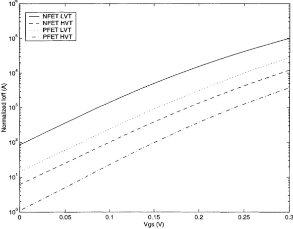
VGSFigure 2-1 shows the simulated subthreshold current versus VGS for the four FETs
used from the 0.13pm process. The HSPICE simulation that produced this data operated at a temperature of 25C. Each device has the minimum length of 0.13pim
and a set width. The supply voltage for the simulation was
1.OV.
The current throughthese devices was measured over a range from VGS = 0 to VGS = 300mV. The 300mV
number approximates the upper edge of the subthreshold region for the devices.
10 10 104 0 N 0 Z 10 2 10'1 1001: 0 0.05 0.1 0.15 0.2 Vgs (V)
Figure 2-1: Subthreshold Current vs VGS
0.25 0.3
The normalized plot shows that both PMOS and NMOS low VT devices have subthreshold currents more than an order of magnitude greater than their high VT counterparts at VGS = 0. For both NMOS and PMOS, this ratio rolls off slightly
closer to the threshold voltage.
2.3.1
Subthreshold Slope
Several parameters are necessary for comparing the BSIM2 model to the simulated results. The parameters that are not readily available are y, 77, and n. This device characterization uses single devices, so the body effect does not come into play. We
- NFET LVT
- - NFET HVT
-.-.- PFET LVT
- PFET HVT
describe in a following section how we estimated the value of q. Extracting the subthreshold slope from the simulations allows us to find a valid n for use in the model.
The tailing off of current in Figure 2-1 indicates that the subthreshold current does not increase as rapidly with gate voltage as VGS nears the threshold voltage. In other words, the subthreshold slope increases along with VGS. Taking the derivative of the curves in Figure 2-1 and inverting the result provides an instantaneous estimate of the subthreshold slope at each value of VGS.
104 103
z
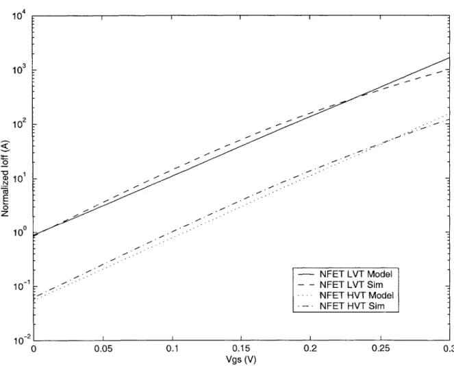
10 2 10 N 0 z 100 -1---NFET LVT Model 10 -- NFET LVT Sim **NFET HVT Model NFET HVT Sim 10-2 0 0.05 0.1 0.15 0.2 0.25 0.3 Vgs (V)Figure 2-2: Model versus Simulation for Varying VGS
The "instantaneous" value of n can be derived by applying Equation 2.2 to the subthreshold slope data. Selection of n makes a considerable difference in the model
since Equation 2.1 depends exponentially on n. The value of n varies rather widely across the VGS range. Experimentation showed that a value of n from lower VGS values provided a close match between the model and the simulated results. This value of n also is the mean value of the data for n over the lower range of VGS. Neglecting the data from the higher gate voltages presumably gave a more accurate estimate for the value of n because the neglected range of n corresponds to the devices beginning to leave the subthreshold region.
Figure 2-2 shows that the normalized BSIM model for subthreshold leakage matches well with the simulated results for the NFETs. The PFET models showed similar matching accuracy. The models used the value of n determined using the above method. The next section describes the process for determining rq.
2.4
VDS
and the DIBL Coefficient
Equation 2.1 shows that the leakage current of a FET in subthreshold depends on the supply voltage in two ways. First, the leakage current rolls off exponentially with
VDS due to the term in parentheses, 1 - e 1
th . This term only becomes noticable
at low values of VDS. The leakage current also increases exponentially based on VDS.
The coefficient that weights the exponent is the DIBL facter. Drain Induced Barrier Loading (DIBL) refers to the effective reduction of threshold voltage with an increase
of VDS. This occurs in short channel devices because the depletion regions around
the surce anu the drain junctions can' e reasonaly large relative to e channel
length. Increasing VDS causes an increase in the depletion regions at the source and drain which allows a smaller VGS to invert the channel.
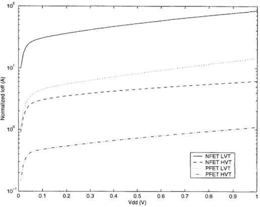
102 10' 0 N 0 z 100 10-1 0 0.1 0.2 0.3 0.4 0.5 Vdd (V) 0.6 0.7 0.8 0.9 1
Figure 2-3: Simulation of Subthreshold Leakage versus VDS
Figure 2-3 shows simulated data for all four types of FETs. Sweeping from a small value to the full value of 1V shows the dependence of the leakage
--- NFET LVT -- NFETHVT PFET LVT PFET HVT the VDS currents
on VDS. The parenthetical term from the equation mentioned previously models the rolloff of the current that appears at extremely low voltages. The slope of the current over the rest of the voltage range arises from the DIBL effect.
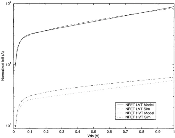
Once all other parameters in the BSIM2 model were determined, sweeping q pro-vided an easy method for matching the DIBL coefficient. Experimentation allowed a choice of q that made the slope of the curve for the model match the simulation data. Figure 2-4 shows the results for the NFETs. The data for the PFETs was similar. The figure shows that a careful selection of q permits a close match in the slopes of the model and the simulation data. The slight offset for the high VT device occurs because the model did not match as well at the VGS = 0 and VDS = IV point (see Figure 2-2). 10 2 2 10 .N 0 NFET LVT Model - NFET LVT Sim .... NFET HVT Model NFET HVT Sim 10 0 0.1 0.2 0.3 0.4 0.5 0.6 0.7 0.8 0.9 1 Vds (V)
2.5
Temperature
10
-FNF-T L-T
20 0 50 T0 70 C8 90 100 110 120
Teffperalu0. (C)
Figure 2-5: Simulation of Subthreshold Leakage versus Temperature
Figure 2-5 shows simulated data for leakage current versus temperature for all four types of FET. The models required no special attention to portray the effects of temperature on subthreshold current accurately. As expected, the subthreshold leakage increases exponentially with temperature. The exponential increase comes from the Vth in the denominator of the exponent in Equation 2.1, where Vth
-q
The exponential rate of increase with temperature increases further due to the V in the expression for 1. Figure 2-6 shows the models versus simulations for the NFETs.
NFET LOT Model NFET LO So 10'
20 30 40 50 '0 70 0 90 0 110. 120
Temfperature (C)
2.6
Subthreshold Leakage Versus Device Size
Both the first order model in Equation 1.1 and the BSIM2 model in Equation 2.1 show a simple linear relationship between device size and subthreshold leakage cur-rent. The equations predict that the leakage current will increase in proportion with device width. Similarly, the leakage current is inversely proportional to device length. Extensive research has shown the inability of these lower order equations to model device behavior for short and/or narrow devices.
102 101 0 0 N o 0 z 10 10 5 10 15 20 Normalized Width 25 30
Figure 2-7: Threshold Voltage Variation with Device Size
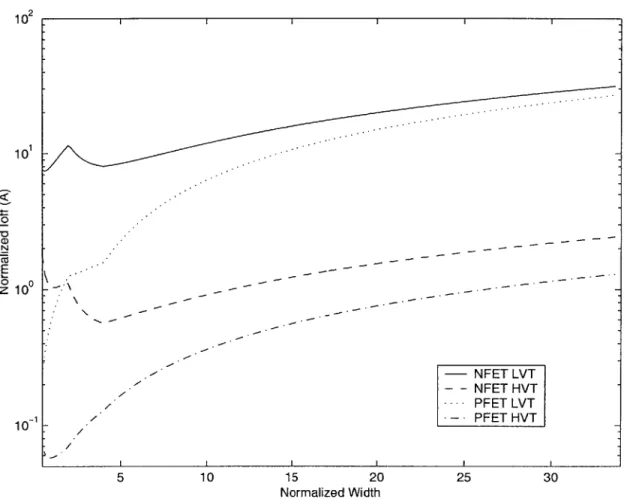
Figure 2-7 shows the simulated leakage current varying with device width in the 0.13prm CMOS process. The first order, proportional relationship between width and leakage current begins to emerge only when the width becomes relatively large. The relationship at lower widths clearly is not linear. Instead, lowering width produces
- NFET LVT
-- NFET HVT
-.-. PFET LVT
a brief rise in current followed by a more dramatic tail-off. These two effects can produce a pronounced peak as in the case of the low VT NFET, or they can appear more as ripples in the current plot as in the case of the PFETs. In either case, the higher order effects on leakage current can cause headaches for circuit designers.
NFET low VT NFET high VT
r-4 -2 22. 0 Z 2 2 1.5 1.5
Normalized length 1 1 Normalized width PFET low VT 03, 0 2 2 1.51.
Normalized length 11 Normalized width
4-4
3
-22
rm 2 1.5 15
Normalized length 11 Normalized width PFET high VT 3-- 1-2 N2 1.51.5
Normalized length 11 Normalized width
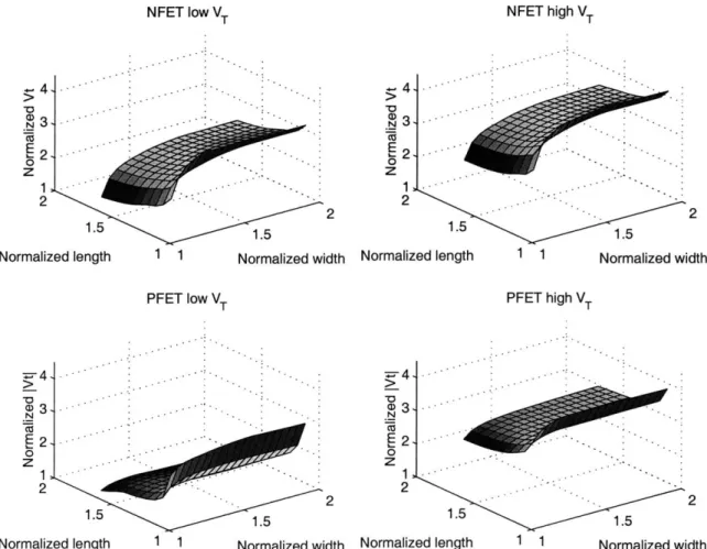
Figure 2-8: Threshold Voltage Variation with Device Size
Device research has characterized these effects for short, narrow devices. The leakage current at narrow widths changes because the effective threshold voltage changes. Figure 2-8 shows the simulated variation of threshold voltage with device size. The axes in the four plots are the same to facilitate comparison. For every one of the devices, the threshold voltage increases as length decreases, and VT decreases as width decreases.
Effect that suggests that VT will decrease for a shorter length device. Appropriately, the relationship between VT and length exhibited in Figure 2-8 is called the Reverse
Short Channel Effect (RSCE). Several methods exist for modeling the RSCE (i.e. -[21, 22]). The RSCE occurs because of a pile-up of dopant material (e.g. boron) along the edges of the source and drain. As the channel shortens, the pile-ups of dopant at the channel edges begin to overlap. This increases the effective channel doping value and leads to the increase in threshold voltage.
The decrease in VT with decreasing width is called the Reverse Narrow Channel Effect (RNCE). Existing work attributes the RNCE to transient enhanced diffusion
(TED) that redistributes dopant material (e.g. boron) away from the isolation oxide along the edges of the channel [23]. When the device width decreases, the lower concentration of dopant along the edges of the channel extends across more of its width. This reduces the effective doping of the channel and reduces VT. The TED is the same mechanism that causes the dopant pile-up at the edges of the source and drain to cause the RSCE.
The RNCE explains the abnormalities that appear in the leakage current plot in Figure 2-7. As device width lowers, the leakage currents decrease with width but increase due to a lowering VT. The combination of these effects produces the simulation results in the figure.
These variations in subthreshold current with device size have at least one inter-esting practical consequence for circuit design in this process. The minimum sized high VT device is no longer minimum sized in the traditional sense. Figure 2-7 shows that the minimum leakage current for the high VT NFET occurs at a width of about
4 times minimum size. A high VT NFET of this size has a larger on-current than a
minimum sized device, but its off-current is several times less. For this reason, the "minimum sized" high VT devices in the testchip are actually about 4X the minimum physical size.
Chapter 3
Voltage Scaling During Standby
Mode
3.1
Introduction
This chapter proposes scaling the supply voltage during standby mode. MTCMOS circuits using LFBFFs could save power while retaining state in standby mode by using a reduced supply voltage. Lowering the voltage supplied to the sequential logic reduces power directly (P=VI). It also reduces the leakage currents drawn by the flip-flops. This chapter examines the limits of supply voltage scaling for LFBFFs. It also proposes a method for adaptively adjusting the supply voltage to sequential logic during standby mode.
3.2
Voltage Scaling Concept
The leakage feedback flip-flop (LFBFF) proposed in [19] has the ability to hold its state in standby mode, using a mismatch in leakage currents, even when its inputs float. This mechanism for memory retention should continue to function correctly
even with lower supply voltages.
MTCMOS circuits using LFBFFs could save power while retaining state in standby mode by using a reduced supply voltage. Different regions of a circuit permit
differ-ent depths of voltage scaling. For example, the power supplied to combinational logic can be disconnected entirely. Sequential logic needs to remain powered to hold state. Lowering the voltage supplied to the sequential logic reduces power directly (P=VI) and by reducing leakage currents. These operations would eliminate subthreshold leakage in the combinational logic and dramatically reduce standby leakage power in the sequential logic.
3.3
Varying Supply Voltage and the LFBFF
A given implementation of LFBFFs has a lower bound on the supply voltage below
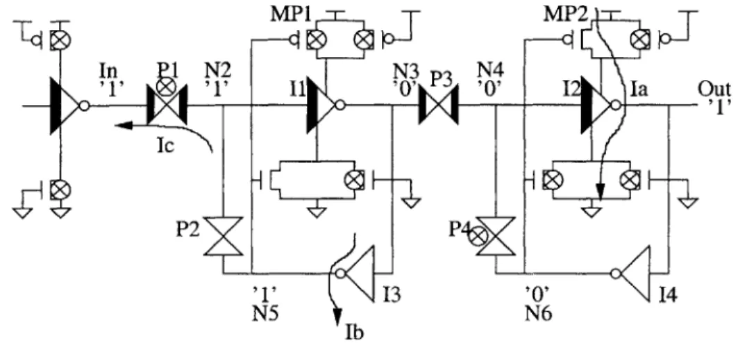
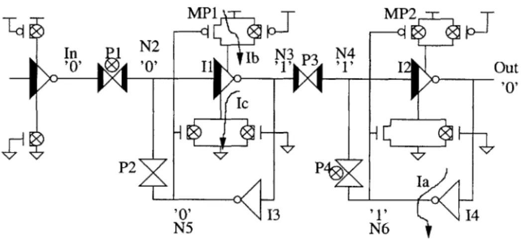
which the device cannot hold state. Figure 3-1 shows the LFBFF in sleep mode with
1 P3
in N2 N3 N4 Out
P2
N5 I3 N6 I4
Figure 3-1: LFBFF in Sleep Mode
an input inverter. The following two sections describe the LFBFF holding state with lower supply voltage. The sections detail the mechanism of failure for each storage value.
Figure 3-1 implicitly includes a few signals that deserve mention. The sleep devices connected to the sleep and sleep signals appear in the figure with their gates tied to power and ground, respectively. The discussion in this chapter assumes that the sleep signal remains at the full VDD value of one volt throughout any voltage scaling. This is true for all of the simulations described in the chapter. The sleep voltage remains high to simplify analysis since the high sleep signal drives the PMOS sleep
devices with a negative VSG when the supply voltage decreases. This decreases the subthreshold current in those devices to a negligible value. Since the sleep signal is routed with its own power supply on the testchip (see Chapter 5), the sleep signal can scale along with the flip-flop voltage. The analysis of power savings in the conclusion shows that scaling the sleep power supply degrades the ability of the flip-flops to hold state at a low voltage but increases overall power savings. Figure 3-1 also shows the on or off state of the passgates. The clock and clock signals determine the state of the passgates. Since the testchip employs MTCMOS gates to drive the clock signals, the logical high clock will take on the reduced supply voltage value of the flip-flop supply during voltage scaling. The In node also scales with the flip-flop power supply because the input buffer lies in the flip-flop power region.
3.3.1
Storing a Logic '1'
The flip-flop maintains the correct state as long as the nodes in the circuit all maintain the correct logical values. Table 3.1 shows the state of the nodes in the flip-flop for a stored logic '1'. The nodes that should retain a '0' value have no trouble doing so as
Table 3.1: LFBFF State for Stored '1'
VDD scales so long as the logical '1' nodes remain correct. The logical '1' nodes are
the initial point of failure for the flip-flop as the power supply lowers.
As Table 3.1 shows, there are two key nodes for storing a '1' that need to retain the high value. These are the N2/N5 node and the output node. Figure 3-2 shows the schematic of the flip-flop holding this state. This initial analysis assumes that
Node Name Value
N2 '1' N3 '0' N4 '0' N5 '1' N6 '0' Out '1'
MP1, MP2, and inverters 13 and 14 are all minimum sized. Sizing these devices for
minimum subthreshold leakage makes sense because they do not have to be large for active mode operation. This analysis will show, however, that their sizes can dictate the minimum voltage supply during voltage scaling.
MP1 MP2 In, I N2 N3 N4 '1 '0' I Ia Out'1' I C P2 P '1'13 '1 4 N5 N6 Ib Figure 3-2: LFBFF Holding a '1'
First consider the output node holding a '1'. The output will remain a logical '1' as long as MP2 can supply all of the current drawn through the two NMOS sleep devices with VSD(MP2) ~ 0. Note that the current through the other PMOS sleep device is negligable because its VSG becomes strongly negative as VDD scales and
sleep remains at 1 volt. The combined width of the NMOS sleep devices in the slave
latch increases their subthreshold current relative to the current supplied through the minimum sized MP2. The source to gate voltage of MP2 also decreases with the power supply voltage. As the voltage supply drops, MP2 eventually transitions from the linear region to the subthreshold region. The combination of these effects eventually decreases the amount of current MP2 can support (with VSD = 0) below
the current supported by the NMOS devices. Since I, in Figure 3-2 goes through both MP2 and the NMOS sleep FETs, MP2 must increase its VSD to maintain the current balance. Once this happens, the voltage at the output node begins to fall at a faster rate than the decreasing supply voltage.
- VPWR
0.1-0.05
2 3 4 6
Time (s)
.I-Figure 3-3: Output Node Changing Value for Stored '1'
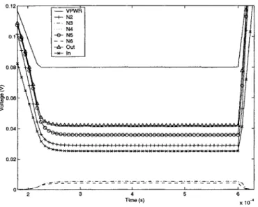
with a supply voltage of just above 100mV. At this value of VDD, the circuit just
barely fails, so it takes some time for the voltage values to settle before they cause the output node to change its logical value. The figure shows that node N6 begins to increase its voltage value well before the latch actually fails. As the output node
voltage (input to 14) begins to drop below the VDD value, the PMOS in inverter
14 begins to increase its subthreshold current as the NMOS in 14 loses some of its current drive. Node N6 must rise above zero to balance the current in the inverter. The increase of N6 aggravates the situation with I, by reducing the gate drive for MP2 and increasing the gate drive of the NMOS sleep device. This feedback adds to the inability of MP2 to sustain I, without the output voltage dropping even more.
A similar situation causes the logical '1' at node N5 to transition to '0'. Figure 3-2
shows two currents, lb and I,, that act to pull node N5/N2 toward ground. Current
Is occurs because of the inability of the minimum sized PMOS inside inverter 13 to sustain the leakage current drawn by the NMOS device in that inverter without an
increased VSD. Similar to the process described above, N5 drifts below the VDD value.
Another current mismatch in the sleep devices for the input buffer causes node IN
to begin to fall below VDD. This falling voltage pulls node N2 toward ground by the
large leakage current, Ic, through the low VT passgate P1. The combined effects of Ib
- VPWR -+-N2 -N3 -6,- NS 0.16 2 3 4 5 6 Tim (a) s
10-Figure 3-4: Internal Node Changing Value for Stored '1'
occurring during the same simulation that produced Figure 3-3.
The combinations of the effects in these two figures result in the failure of the
flip-flop to maintain a logical '1' below - 1OOmV. However, the mechanisms of failure
suggest that the performance of the flip-flop can improve. For example, increasing the width of MP2 above minimum size could allow that FET to sustain the large leakage current Ia without requiring a larger VSD. Additionally, increasing the size of the PMOS device in inverter 13 would hold N5 at a logical '1' for lower supplies. The sleep devices for the input buffer were sized for speed reasons during active mode, so they cannot be changed. Figure 3-5 shows the re-sized LFBFF correctly holding a logical '1' at a supply voltage of 80mV. Note that the output node and all the internal voltages settle to a steady state at the lower supply voltage and then return to the proper levels when the supply voltage rises again. The steady state values of the logical '1' nodes actually are well below VDD at the lower supply voltage. Nevertheless, the nodes all return to the correct logical values when the supply voltage returns to higher values. This plot shows that careful sizing of the devices mentioned above can improve the ability to store a '1' at lower supply voltages. The next section will show that tradeoffs with storing a logical '0' prevent the improvements from going much
0.12 0.1 0.08 0O06 0.041 0.02 2 3 4 Time (s) 5 6 0 10 Figure 3-5: LFBFF Storing '1' at VDD = 80mV
3.3.2
Storing a Logic '0'
The LFBFF consisting of minimum sized MP1, MP2, 13, and 14 stores a '0' success-fully at extremely low VDD values. Modifications made to improve the storage of a logical '1' degrade the ability of the flip-flop to store a logical '0'. These modifications consisted of upsizing MP2 and the PMOS device inside inverter 13. These changes directly address the causes of failure described in the previous section. Table 3.2 shows the state of the nodes in the flip-flop for a stored logic '0'. Again, the nodes
Table 3.2: LFBFF State for Stored '0' Node Name [Value
N2 '0' N3 '1' N4 '1' N5 '0' N6 '1' Out '0'
in the flip-flop that deserve the most attention are those holding a logic '1'.
Figure 3-6 shows the LFBFF holding a logical '0'. As the supply voltage begins
, - -VPWR
- 9 N -- N
In P1 N2 P2_X MP2 I Out '' Ia '1' 14 N6 Figure 3-6: LFBFF Holding a '0'
to fall, the voltage at node N6 also falls. The current I, in the figure shows the mechanism that causes the N6 voltage to fall below VDD. As previously discussed, the PMOS inside inverter 14 cannot support the leakage current through the NMOS
device at lower supply voltages without increasing its VSD.
Figure 3-7 shows how the size of the PMOS in 14 affects the steady-state voltage
0 50 100 150 200 VPWR (m~V)
Figure 3-7: High VT Inverter Output for Varying Widths
of N6. The figure shows the voltage at N6 for a standalone high VT inverter with a few different widths for the PMOS. The input of the inverter is grounded explicitly for each case, and the outputs show the DC output of the inverter as VDD scales toward
0. The plot indicates that the output of inverter 14 will begin to have a voltage
_VPWR -A- Pw=mi 0- -- Pwid min+2u 0 0-~ 20 1 5 10 5 260 MP1 bIb N3 P3N4 'b I 3 91 N5
lower than the supply voltage once VDD decreases beyond - 1OOmV. A smaller width
PMOS in the inverter creates a much wider gap between the output voltage (N6) and the supply voltage.
Once the voltage at N6 begins to drop, MP2 will see increased gate drive, and the
NMOS sleep device will lose gate drive. As a result, the voltage at the output will
rise above zero to maintain the match between the PMOS and NMOS currents. As shown in the previous section, the rising output voltage aggravates the effect shown in Figure 3-7 (where the input was grounded). The resulting feedback continues to drive N6 to an even lower voltage. Now it is apparent that increasing the size of MP2 to help the flip-flop store a logical '1' (as in the previous section) will cause the flip-flop to fail earlier while storing a '0'. This tradeoff requires that MP2 be sized with care so that the flip-flop fails for both a '1' and '0' at approximately the same voltage.
Figure 3-8 shows this failure occurring for a stored '0'. The plot shows waveforms for a LFBFF sized with minimum width 14 and MP1 but with increased MP2 and 13 PMOS to help with the store '1' case. The plot shows node N6 falling below the low
supply voltage value of - 80mV. As it falls, the output voltage begins to rise slightly.
The voltages continue to settle, and N6 eventually dives for 0 while the output node gets pulled high. When the supply voltage returns to a higher value, the output node clearly tracks it as a logical '1'. Node N4 in the plot also contributes to flipping the state of the output. As N4 falls (the reason for this follows shortly), the low VT
PMOS inside inverter 12 increases its subthreshold current, and the NMOS in that inverter supports less current. This only helps MP2 to charge up the output node.
The other node that will cause failure for the LFBFF storing a '0, is N3. The same effects that caused the output node to fail for a storing '1' case will cause N3 to change to a logic '0'. We summarize those reasons again for this case. The voltage at node N3 falls along with the supply voltage. It actually begins to fall below the supply voltage because of the current mismatch that develops between Ib and I,. In other words, voltage N3 must drop below VDD in order for lb to equal I. When it