Circuit Design and Technological Limitations of
Silicon RFICs for Wireless Applications
by
Donald A. Hitko
Bachelor of Science in Electrical Engineering GMI Engineering & Management Institute, 1994
Master of Science in Electrical Engineering and Computer Science Massachusetts Institute of Technology, 1997
Submitted to the Department of Electrical Engineering and Computer Science in partial fulfillment of the requirements for the degree of
Doctor of Philosophy in Electrical Engineering and Computer Science at the
MASSACHUSETTS INSTITUTE OF TECHNOLOGY June 2002
@ Massachusetts Institute of Technology, 2002. All Rights Reserved.
A
Author
Department of Electrical Engineering and Computer Science May 24, 2002
Certified by _
Charles G. Sodini Professor of Electrical Engineering and Comyuter Science Thesis Supervisor
Accepted by
Arthur C. Smith Chairman, Committee on Graduate Students Department of Electrical Engineering and Computer Science
BARKER
MASSACHUSETTS INSTITUTE
OF TECHNOLOGY
JUL 3 12002
LIBRAR IESCircuit Design and Technological Limitations of Silicon RFICs
for Wireless Applications
by
Donald A. Hitko
Submitted to the Department of Electrical Engineering and Computer Science on May 24, 2002, in partial fulfillment of the requirements for the degree of
Doctor of Philosophy in Electrical Engineering and Computer Science
Abstract
Semiconductor technologies have been a key to the growth in wireless communication over the past decade, bringing added convenience and accessibility through advantages in cost, size, and power dissipation. A better understanding of how an IC technology affects critical RF signal chain components will greatly aid the design of wireless systems and the development of process technologies for the increasingly complex applications that lie on the horizon. Many of the evolving applications will embody the concept of adaptive per-formance to extract the maximum capability from the RF link in terms of bandwidth, dynamic range, and power consumption-further engaging the interplay of circuits and devices is this design space and making it even more difficult to discern a clear guide upon which to base technology decisions. Rooted in these observations, this research focuses on two key themes: 1) devising methods of implementing RF circuits which allow the per-formance to be dynamically tuned to match real-time conditions in a power-efficient man-ner, and 2) refining approaches for thinking about the optimization of RF circuits at the device level. Working toward a 5.8 GHz receiver consistent with 1 GBit/s operation, signal path topologies and adjustable biasing circuits are developed for low-noise amplifiers (LNAs) and voltage-controlled oscillators (VCOs) to provide a facility by which power can be conserved when the demand for sensitivity is low. As an integral component in this effort, tools for exploring device level issues are illustrated with both circuit types, helping to identify physical limitations and design techniques through which they can be miti-gated. The design of two LNAs and four VCOs is described, each realized to provide a fully-integrated solution in a 0.5 pm SiGe BiCMOS process, and each incorporating all biasing and impedance matching on chip. Measured results for these 5-6GHz circuits allow a number of poignant technology issues to be enlightened, including an exhibition of the importance of terminal resistances and capacitances, a demonstration of where the transistor fT is relevant and where it is not, and the most direct comparison of bipolar and CMOS solutions offered to date in this frequency range. In addition to covering a number of new circuit techniques, this work concludes with some new views regarding IC technol-ogies for RF applications.
Thesis Supervisor: Charles G. Sodini
Acknowledgments
Wow! Maybe that says it all. I can remember when it took me by surprise to hear a colleague mention taking five years to complete the Ph.D.-five years after the Master's, that is. How little I knew then what deciding to continue beyond the Master's would entail for me. But I recall another colleague attributing his decision to stay for the Ph.D. pro-gram to thinking: "It seemed like a pretty neat place to spend a few years." Albeit at a dif-ferent location, and although "a few years" may have proven to been a euphemism, I still found his statement to hold throughout my time here.
Attending graduate school at a university like MIT is mostly about the people that it brings together, for this is what makes the experience so rewarding. But rather than implicating anyone, I would instead like to express my gratitude to each of you by men-tioning some of your personal contributions which have meant so much to me. So here goes, in no discernible order. First, thank you for assuring me that I was born to be a grad-uate student. How right you were. Thank you for the Tosci's runs, and for being around the group almost as long as I have been. Thanks to those who collectively surmounted the phenomenon of always playing one bad inning. Thank you for the time spent crushing tennis balls, and for waiting in perpetuum for a window seat. Thanks for getting together to work on calendar pages, and to the many predecessors here who were featured in those pages. Thanks to those with whom hallway hockey was anointed. Perhaps we can have a reunion in 30 years to see if the puck is still there. Thank you for the many helpful job-related discussions, for sustaining some semblance of organization about the office, for always being upbeat, and for infusing new enthusiasm into the group. Thanks to those who provided helpful advice on FFTs, replica biasing techniques, device noise, pointy-haired pursuits, computers, the art of Re-use, RF circuits, and when to shoot the puck. My apologies if I did not do particularly well in taking the advice. Thank you for the die photos, which dressed up numerous presentations as well as this thesis. Thanks to those who made playing (and coaching!) hockey so much fun, and to those who put up with me taking their P.E. classes six times. Of course, this would not have happened without the initial encouragement to get started on the hockey "hobby", for which I am very thankful. Thank you for always putting on a good show whenever I came to watch, and for coming to watch my feeble efforts. Thank you for the Esplanade skates, and especially those at 2AM. Thank you for getting up at 4AM to observe re-enactments of historical events. Finally-although still in no discernible order-thank you for the lAM dinners (of which Mom would not approve) and for ice cream in (on?) fire trucks; I'm glad I could be there for your 48th.
In their support of this work, we are indebted to SRC (through contract number 2000-HJ-794), IBM Microelectronics in Burlington, Vermont, and HRL Laboratories in
Acknowledgments
Malibu, California. With a big assist from Jeff Gross, the folks at IBM supplied some excellent focused-ion beam rework to enable experimentation with the oscillators. HRL lent their support through a fellowship, making space for me on two of their IC fabrication runs, providing access to noise measurement equipment for amplifiers and oscillators, and by continually demonstrating their remarkable patience.
The readers of this thesis have proven nothing short of amazing, a task made even more daunting by my manner of writing and lack of a knack for timing. A big thank you to Charles Sodini, Jesu's del Alamo, Hae-Seung Lee, and Dan McMahill, each of whom are undoubtedly grateful that FrameMaker® has no provision for footnoting a footnote. In particular, Charlie deserves a commendation for being dragged through this procedure on my behalf with two theses and an area examination. Discussions with Jesds regarding devices and noise have always been very enlightening. I am also very appreciative of the time Dan has spent on this, as he has offered a great deal of insight and many suggestions which are reflected throughout this work.
Of course, none of this would have occurred without the unwavering support of my family. To my parents, may you both enjoy a relaxed forthcoming Father's Day (Mother's Day wishes were passed along in my Bachelor's thesis) and a happy (upcoming) 36th anniversary. I'd also like to congratulate Trisha and Eric for their perseverance, and wish you continued good tidings with the restaurant. Finally, many thanks are owed to the rest of the family for keeping up with me during my extended disappearance to Massachusetts. As for what comes next, well, we will have to see. But as a start, the late "Badger" Bob Johnson might have said it best in noting, "It's a great day for hockey." Sounds good to me.
Donald A. Hitko
Cambridge, Massachusetts May 29, 2002
Table of Contents
Acknowledgments 5
Introduction 15
1.1 Thesis C ontributions ... ... 17
1.1.1 Optimization of RF Circuits at the Device Level ... 18
1.1.2 Trade-off Between Quality of Service and Power Consumption ... 19
1.2 A Preview of the T hesis... ... ... 21
An Approach to Spiral Inductor Modeling 23 2.1 Integrated Inductances ... 24
2.2 Selected Recent Efforts in Spiral Inductor Modeling ... 25
2.2.1 Alternative Inductance and Series Resistance Formulations ... 30
2.3 Spiral Inductor Loss Mechanisms...33
2.3.1 Inductor Q uality Factor... 35
2.4 Quick Turn Models for Spiral Inductors... 37
Appendix: Calculation of Inductor Quality Factor ... 40
Time-Variant System Modeling 43 3.1 A Plausibility Argument for Time-Variant Models...44
3.2 Oscillator Analysis Using a Linear Time-Variant Model...47
3.3 Optimizing Devices and Technology for Oscillators... 51
3.4 C yclostationarity in O scillators... 55
3.5 Extending the Linear Time-Variant Model to Mixers ... 65
Low-Noise Amplifiers 73 4.1 Im pedance M atching... .... 74
4.2 Technology Considerations for LNAs...79
4.3 A lternative LN A Topologies ... 83
Contents
4 .3 .2 C asco d e ... 8 9
4.3.3 Effects of Inductor Loss... 91
4.4 Transistor and Amplifier Stability ... 93
4.5 Lessons in Low Noise... 98
Appendix: Two-port Stability Circles...100
An Exercise in Designing Low-Noise Amplifiers 101 5.1 A Bipolar 5.8 GHz LNA Design ... 102
5.1.1 Output Matching Network Design...103
5.1.2 Operating at Reduced Power Consumption Levels ... 110
5.1.3 A Switched Current Source Bias Circuit ... 116
5.1.4 Layout Design of the 5.8 GHz Switched-Stage LNA ... 123
5.2 CMOS LNA Design...126
5.2.1 Noise in CMOS Transistors ... 127
5.2.2 A 5.8 GHz CMOS LNA ... 130
5.2.3 Stabilized Biasing for the CMOS LNA ... 133
5.2.4 Layout Design of the 5.8GHz CMOS LNA ... 137
5.3 Measured Results for the 5.8 GHz LNAs...139
5.4 Lessons in Low Noise: The Sequel...150
An Experiment with Voltage-Controlled Oscillators 155 6.1 A Family of Bipolar 5.8GHz VCOs ... 156
6.1.1 Transistor Considerations in Oscillators...158
6.1.2 A Differential Colpitts Oscillator...161
6.1.3 Biasing Circuitry for the Bipolar Oscillators ... 164
6.1.4 An Impedance-Matched Output Buffer ... 165
6.1.5 Layout Design of the Bipolar VCOs...169
6.2 A CMOS 5.8 GHz VCO Design...171
6.2.1 Adaptive Biasing of the CMOS Oscillator ... 173
6.2.2 An Impedance-Matched Output Buffer in CMOS...178
6.2.3 Layout Design of the CMOS VCO...179
6.3 Measured Results for the 5.8 GHz VCOs...181
6.4 Observations on Oscillators ... 191
Final Thoughts 195
List of Figures
1-1 System dynamics model for IC technology-based markets...16
2-1 Coupled line segment model proposed by Long and Copeland [12]. ... 26
2-2 Compact lumped-element model for an inductor on a silicon substrate. ... 27
2-3 Loss m echanism s in a spiral inductor... 34
2-4 Geometry parameters describing a square spiral inductor...38
2-5 Circuit model for calculation of inductor quality factor...40
3-1 Pictorial argument for a time-variant oscillator model, adapted from [34]...45
3-2 Simplified schematic of a single-balanced mixer...46
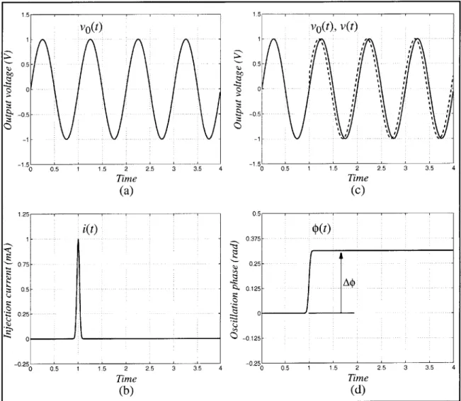
3-3 Calculation of the impulse sensitivity of an oscillator; (a) steady-state oscillation voltage, (b) current injected to approximate an impulse function input, (c) impulse perturbation response compared with the steady-state oscillation, (d) phase of the output signal in the perturbation response. ... 48
3-4 Typical oscillator impulse sensitivity function... 50
3-5 Schematic of single-ended oscillator used in noise analysis...52
3-6 Bipolar transistor with terminal parasitic elements...53
3-7 ISFs associated with transistor terminal resistances...54
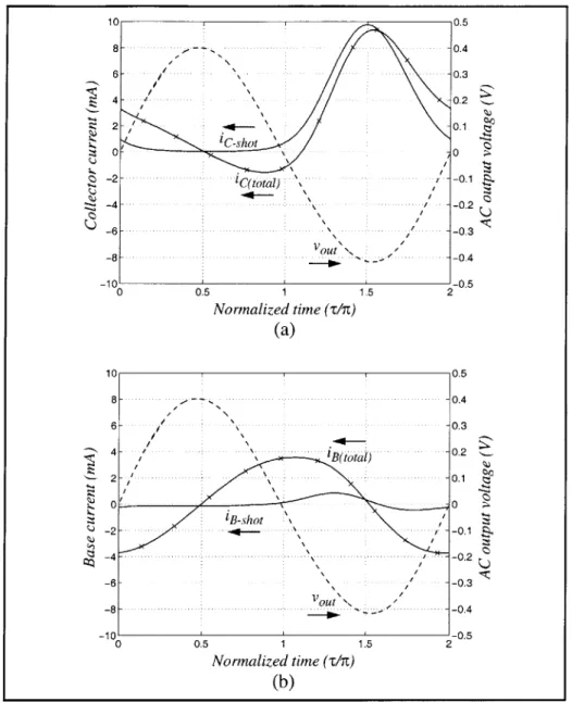
3-8 Transistor collector (a) and base (b) currents calculated for the single-ended oscillator example; the terminal currents are marked with x's and the components that generate shot noise are shown with the solid traces. ... 56
3-9 Schematic used to solve for the transistor displacement currents in the single-ended oscillator exam ple ... 58
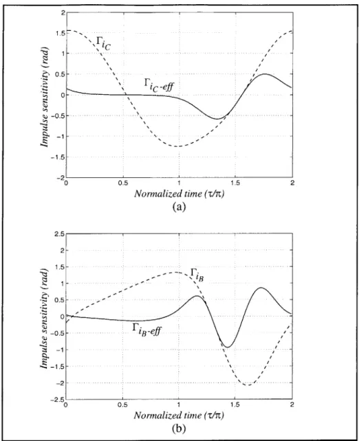
3-10 Calculation of the effective ISFs for the collector (a) and base (b) shot noise sources for the single-ended oscillator example. ... 60
3-11 Calculation of phase noise for single-ended oscillator example. ... 61
3-12 Demonstration of the potential effect of transistor displacement currents in the calculation of oscillator phase noise ... 63
Figures
3-14 Calculation of the impulse response of a mixer; (a) impulse perturbation response compared with the steady-state condition, (b) applied impulse and calculated
im pulse response... 67
3-15 Mixer response to noise injected at the input of the switching pair; (a) response to impulses injected at moments throughout one LO period, (b) 2-D DFT of impulse response data giving conversion gain for noise about each LO harmonic as a function of the chosen IF . ... 68
3-16 SPICE statement for a periodic current impulse. ... 69
3-17 Calculation of the noise in a mixer resulting from the input transconductor; (a) conversion gains from input of switching pair to an IF output at 800MHz, (b) equivalent output current noise from RF transconductor stage. ... 70
4-1 Input impedance-matching using an emitter inductance in a common-emitter amplifier stag e . ... 7 7 4-2 Effect of emitter inductance on the input impedance of a common-emitter amplifier stage where the arrows indicate the direction of increasing LE; correlation in the equivalent input noise sources has been neglected... 78
4-3 Illustration of achieving a simultaneous noise and power match in a common-emitter transistor stage; correlation in the equivalent input noise sources has been n eg lected . ... 8 3 4-4 B attjes' fT doubler circuit. ... 88
4-5 Cascode amplifier stage with input impedance matching. ... 90
4-6 Intrinsic feedback within a common-emitter stage... 90
4-7 Source stability circles for a common-emitter transistor...94
4-8 Loop gain analysis of a common-emitter transistor. ... 95
4-9 Load stability circles for an emitter-follower transistor. ... 96
5-1 Cascode stage tuned for minimum noise at 5.8 GHz. ... 102
5-2 Design of the output matching network for the cascode LNA stage...104
5-3 Cascode LNA gain stage tuned for 5.8 GHz...107
5-4 Evolution of noise figure (a) and gain (b) in a cascode LNA stage as inductor loss (Qs of 17-19) is included. In (a), the upper trace of each pair is the 50 noise figure (NF50) and the lower is the minimum noise figure (NFmi). In (b), each set of traces represents the maximum available gain (Gna) and the available gain (Ga) for the condition listed to the right, where Ga is labeled when it differs appreciably from Gina. By convention, the maximum stable gain (Gms) is shown when Gma is undefined. Marked with the diamonds is 20log s211 for the matched stage when a 50 impedance is provided by both the source and load...108
Figures
5-6 Effects observed in the 5.8 GHz LNA of adding the low power stage and including
parasitics associated with the pads, resistors, and capacitors. ... 115
5-7 Effect of the bias coupling impedance on noise and linearity...117
5-8 Concept for the base current source bias scheme...118
5-9 Biasing circuitry for the switched-stage 5.8GHz LNA...120
5-10 Simulated performance of the 5.8GHz switched-stage LNA in both the (a,b) "high performance" and (c,d) "low power" modes. Note the scale change between the modes in representing the gain and noise figure...122
5-11 Simulated behavior of the 5.8GHz switched-stage LNA over (a) temperature and (b) supp ly v ariation s. ... 123
5-12 Die photo of 5.8 GHz switched-stage LNA IC (CMLNA-SW)...124
5-13 Comparison of models for the minimum noise figure of a common-source transistor at two drain current levels. Solid lines represent results of the Shaeffer model [76] and dashed lines are simulation results using full BSIM3v3 models. ... 131
5-14 RF signal path for the 5.8GHz CM OS LNA...132
5-15 Biasing circuitry for the 5.8GHz CM OS LNA. ... 134
5-16 Simulated performance of the 5.8GHz CMOS LNA in both the "high performance" (a,b) and "low power" (c,d) modes. Noise figure calculations are based upon BSIM3v3 circuit models which have not implemented induced gate noise...135
5-17 Die photo of 5.8GHz CMOS LNA IC (CMLNA-CM)...138
5-18 Measured noise figure (a) and gain (b) of the 5.8 GHz switched-stage bipolar LNA in both the high performance and low power modes. Note the shift in the center frequency of the LN A pass band. ... 140
5-19 Measured s-parameter data for the 5.8GHz switched-stage LNA; the input return loss (a), gain (b), isolation (c), and output return loss (d) are shown. Solid traces indicate the "default" bias conditions for operation at 3 V. Measurements are also provided in the high performance mode for supply voltages of 2V ('o'), 2.5V ('x'), and 4V ( '- ') . ... ... ----. ...--- 14 1 5-20 Measured noise figure (a) and gain (b) of the 5.8 GHz CMOS LNA at three bias current levels. Note the change in scales for the noise figure and gain relative to the switched-stage measurement plots. To improve legibility, Ga has only been shown at the 14 m W setting...143 5-21 Measured s-parameter data for the 5.8GHz CMOS LNA; the input return loss (a),
gain (b), isolation (c), and output return loss (d) are shown. Solid traces indicate the "high performance" bias condition (4.67mA) for operation at 3V. Measurements are also provided as the bias current is reduced to 2mA ('o') and 1 mA ('A') with the 3 V su p p ly ... 14 5
Figures
5-22 Measured input impedance (si1), output impedance (S22) and optimum noise
impedance (1'opt) for the 5.8 GHz switched-stage (a) and CMOS (b) LNAs. Arrows
indicate the direction of increasing frequency...146
6-1 A comm on-base Colpitts-style oscillator circuit. ... 157
6-2 Primary contributions to oscillator phase noise from a transistor sized according to an L T I an aly sis. ... 15 9 6-3 The 5.8 G H z bipolar oscillator core...162
6-4 Biasing circuitry for the 5.8GHz bipolar oscillators. ... 164
6-5 Output buffer for the 5.8 GHz bipolar oscillator family. ... 166
6-6 Simulated phase noise of the 5.8 GHz bipolar VCO operating at 3V and with 6.25mA in the oscillator core...168
6-7 Die photo of the 5.8 GHz bipolar VCO IC (CMVCO). ... 170
6-8 The 5.8 G H z CM O S oscillator core...172
6-9 Biasing circuitry for the 5.8 GHz CMOS oscillator...174
6-10 Simulation of the DC behavior (a) and loop stability (b) of the CMOS oscillator bias circ u it. ... 17 6 6-11 Simulated phase noise of the 5.8 GHz CMOS VCO operating at 3V and with 5mA in the oscillator core...177
6-12 Output buffer for the 5.8 GHz CMOS oscillator...179
6-13 Die photo of 5.8GHz CMOS VCO IC (CMVCO-CM). ... 180
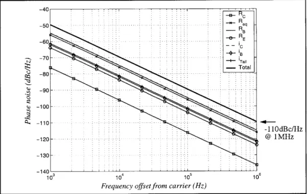
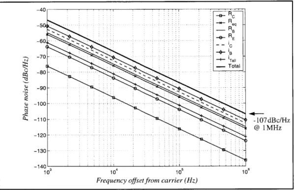
6-14 Measured spectrum and phase noise plots for the bipolar (a,b) and CMOS (c,d) 5.8GHz VCOs operated at 3V. The bias current in the oscillator core is 6mA for the bipolar VCO and 5.2mA for the CMOS version. Note the change in reference level between the spectrum plots in parts (a) and (c)...183
6-15 CMVCO phase noise behavior as a function of bias current and supply voltage, expressed as ratio of carrier power to noise power in a 1 Hz bandwidth located 1 MHz away from the carrier. Operation at voltages above 3 V did not improve the phase noise due to saturation in the biasing circuit...187
6-16 CMVCO-CM phase noise behavior as a function of power dissipation. ... 188
6-17 Technology comparison of phase noise behavior as a function of bias current in oscillator core, expressed as a ratio of carrier power to noise power in a 1 Hz bandwidth located 1 MHz away from the carrier. A 3 V supply has been used for these m easurem ents. ... 190
List of Tables
2.1 Fitting Parameters for GMD Inductance Formulation, from Mohan, et al. [19]...31
5.1 Performance Summary for the C-band Monolithic Low Noise Amplifiers ... 149
6.1 Lumped-Element Model Parameter Summary for the Oscillator Inductor ... 185
Chapter 1
Introduction
One of the largest growth areas in electronics over the past decade has undoubtedly been in applications of wireless communication. Semiconductor technologies have been a key to this growth, bringing added convenience and accessibility through advantages in cost, size, and power dissipation. Wireless products and systems thrive on this increased utility, the commercial momentum of which has been fueling further investment in inte-grated circuit designs and technology. The resulting advancement in system capabilities has developed greater interest and receptiveness on the part of the consumer, leading to more applications being envisioned, and necessitating more available spectrum to support the wireless infrastructure. To obtain this added bandwidth and alleviate interference, the frequencies of the communication channels are necessarily edging upward, placing yet more demands on the technologies used to implement the wireless systems.
Several recently opened ISM bands in the 5-6GHz range have been allocated for unlicensed operation of broadband wireless links between portable devices, computers, and the Internet. While always subject to change, the spirit of these National Information Infrastructure (NII) systems has been described by the FCC in a 1996 ruling [1]:
NII/SUPERNet devices [can] provide short-range, high-speed wireless dig-ital information transfer and could support the creation of new wireless local area networks (LANs) as well as facilitate access to the National Information Infrastructure without the expense of wiring. These devices may further the universal service goals of the Telecommunications Act by offering schools, libraries, health care providers, and other users inexpen-sive networking alternatives which may access advanced telecommunica-tions services.
Three unlicensed bands are set aside by the ruling: 5.15-5.25GHz, 5.25-5.35GHz, and 5.725-5.875GHz, of which the band centered at 5.8 GHz allows the highest transmit power levels. With 150MHz of allotted bandwidth and up to 1W of transmit power, data rates of lGBit/s are conceivable over links covering short haul distances.
Chapter 1: Introduction
While the products and applications in this field are still evolving, the one con-straint is that the consumer market will determine the acceptable end product price based on convenience, functionality, and a comparison with substitutes. Along with a consider-ation of form factor issues, the price the market will bear effectively sets a bound on the technologies which can be used in realizing the product. In conjunction with circuit design techniques, the limitations of these technologies determine the performance that can be achieved in the required system components, a set of capabilities around which the wireless link specifications must be drawn. These specifications in turn define the features and functionality, creating a reinforcing loop in the product design space as illustrated in Figure 1-1.
Price
Features &
I
Circuit
Performance
Technologies
Design
,
Figure 1-1. System dynamics model for IC technology-based markets.
Size and cost constraints may, for example, make the use of a discrete dielectric resonator oscillator impractical for the RF upconversion stage in the transmitter of a port-able communications device. Integrating the RF link within a GaAs or InP MMIC may yield good performance while addressing the size issues, but may represent too costly a solution for the application. A circuit realized in silicon might be a less expensive alterna-tive; however the transistor and passive device parasitics are more significant in a silicon IC technology.1 For an oscillator, the increased transistor terminal parasitics result in a higher phase noise, potentially interfering with weaker signals in adjacent channels or degrading the sensitivity of a receiver.2 In a transmitter, oscillator phase noise can limit
The semiconducting nature of silicon results in appreciable terminal capacitances to the sub-strate (e.g., collector-subsub-strate capacitance in a bipolar transistor) which are not significant when semi-insulating materials are used for the substrate material. Device designs in III-V semicon-ductors also typically employ mesa structures that lower access resistances and junction areas
when compared to more planar device topologies.
Chapter 1: Introduction
how closely channels may be set which, for a fixed bandwidth, reduces the achievable data rate. Conversely, by reducing the signal to noise ratio available to the demodulator, phase noise in a receiver increases the bit error rate. Hence the noise of an oscillator in a wire-less communications system perceptibly impacts the allowable number of users, realizable data rates, and the quality of the link, exemplifying the importance of the device technol-ogy. Making the right technology choice plays a crucial role in determining the commer-cial success of a product.
1.1 Thesis Contributions
Among the realizations from considering the nature of product development is that a better understanding of how an IC technology affects critical RF signal chain compo-nents would greatly aid the design of both wireless systems and future process technolo-gies for the increasingly complex applications that lie on the horizon. The fundamental interplay between devices and circuits in this design space confounds the issue, making it difficult to discern a clear guide upon which to base technology decisions. In designing key RF components-such as oscillators, mixers, and amplifiers-circuit techniques and topologies can be developed to mitigate device limitations and to break traditional design trade-offs by extending the concept of scalable circuit performance in radio transceivers. Furthermore, as the properties of a wireless communication channel tend to be highly uncertain, significant power savings can be realized by using circuits designed to allow a dynamic adaptation to changing operating conditions. In light of these observations, the focus of this thesis centers upon two key themes:
- The optimization of RF circuits at the device level. Two broad classes of circuits are considered in this research: linear time-invariant (LTI) and linear time-variant (LTV). The LTI class of circuits is studied by designing and characterizing a pair of 5.8GHz low-noise amplifiers (LNAs), and the LTV side is investigated by con-structing and measuring a set of four voltage-controlled oscillators (VCOs). Approaches for exploring device level issues are developed with both circuit types, helping to identify physical limitations and design techniques through which they can be mitigated. Other RF circuits, such as mixers, can then be considered through these approaches as a combination of LTI and LTV elements. By carefully crafting an experiment around a set of designs in a BiCMOS process and tracing measured circuit performance back to device level issues, some new views are offered on directions that should be taken in IC technologies for RF applications. - Devising methods of implementing RF circuits which allow the performance to be
dynamically tuned to match real-time conditions in a power-efficient manner. Once the physical limitations are accommodated in the design, extracting the
opti-Chapter 1: Introduction
mum performance from a technology becomes a matter of dissipating the required power in the circuit. It may not, however, be either necessary or feasible to operate the transceiver circuits under this condition at all times. Signal path topologies and adjustable biasing circuits are developed to provide a facility by which power can be conserved in RF circuits when the demand for performance is low, providing flexibility without compromising the operation when optimum performance is required. Incorporation of adaptability at the circuit and system levels is para-mount in expanding the capabilities and increasing the utilization of wireless com-munication links, and yet remains a largely untapped resource in this field.
These themes represent two areas in which innovation will hold significant implications for the future of RF/microwave integrated circuits and the wireless applications in which they are used. An introduction to these ideas and other related concepts is provided in the following sections.
1.1.1 Optimization of RF Circuits at the Device Level
One of the salient characteristics of RF circuit design is that the active devices are often pushed near their physical limits of operation, resulting in a high degree of cor-relation between the performance of an individual transistor and that of the circuit. As the signal frequency increases toward the rate where small-signal gains fall to unity, the ability to compensate device shortcomings through feedback mechanisms becomes constrained. Thus, an important area of investigation for this regime of operation is to identify the device features that are limiting circuit performance in key RF transceiver components. Most of the components can be represented by models of either the linear time-invariant or linear time-variant variety. Through linearity, both models assume that the RF signals being processed are small enough not to appreciably impact the operation of the circuits that are processing them.3 Additionally, in LTI circuits, the parameters of the elements
remain constant-a condition observed in many amplifiers and filters. Time-variant cir-cuits include oscillators, mixers, and prescalers, and are characterized by possessing gains, impedances, noise power, etc., which vary with time-often in a pattern that is periodic. For both classes of circuits, models are discussed as a means of eliciting the mechanisms responsible for constraining the circuit performance. However, this determination cannot be made in a vacuum, as circuit techniques and topologies can be developed to work around limitations (to an extent).4 Pushing the performance envelope in RF can only
hap-pen through a concurrent optimization of circuits and technology.
3 A mixer processes either the RF or IF signal and produces the other; the applied oscillator drive
can be considered as creating a time-varying operating point for the signal and the noise sources in the circuit. More will be said about mixers in Chapter 3.
Chapter 1: Introduction
Knowledge gleaned about the performance-limiting factors identified through these approaches can be applied at a number of levels. First, even within the confines of a chosen process, a designer has considerable latitude with transistor selection, sizing, and 2-D layout geometry. These degrees of freedom may be used to better optimize RF cir-cuits in pushing the limits of a technology, and to make more evident where those limits lie. Similarly, the tools described in this work can be used to guide the selection of a tech-nology for a chosen application. A bipolar or BiCMOS techtech-nology may involve more masks than a comparable CMOS process, but the higher transconductance and lower noise per unit current of a bipolar transistor may provide advantages which can improve the quality of service to cost ratio of the overall system. Knowledge of the technological lim-itations yields insight into the extent to which performance can be expected to benefit. Finally, it is important to understand where device enhancements result in better circuits, and where changes in the device needed to realize the enhancements may hurt perfor-mance more than it helps. A thinner base and higher collector doping concentration can be employed to increase the transistor fT,5 but whether a faster switching response and a higher current gain translate into improved RF circuits can be determined through the models that are proposed in the chapters which follow. Answers to such questions may be surprising, and are vital in setting directions for the continued development of IC process technologies.
As a direct illustration of the impact a transistor technology can have upon RF cir-cuit performance, comparative LNA and VCO designs are implemented in the CMOS and bipolar halves of a BiCMOS process. Different physical limitations are encountered based on the devices being used, and thus different solutions are reflected in the circuits. Each of the designs is geared toward a receiver in a 1 GBit/s wireless network operating at 5.8GHz, for which a high level of sensitivity may be required to support the data rate. But rather than choosing and designing to a given specification, the emphasis here is upon finding the peak performance that can be extracted from a 0.5 m SiGe BiCMOS process, and then determining how these limits change as a function of the technology and power consumption.
1.1.2 Trade-off Between Quality of Service and Power Consumption
To meet consumer expectations in an increasingly sophisticated market, wireless communication systems need to provide an acceptable level of performance under defined
5 The fT of a transistor is the frequency at which its current gain (in the common-emitter or common-source configurations) falls to unity, and is often used as a figure of merit in comparing devices and technologies.
Chapter 1: Introduction
worst-case conditions. The interpretation of acceptability in these networks is one of sup-porting low latency, high data rate, ubiquitous access-necessitating a highly capable link. However, it should be recognized that the data rates will not always be 1 GBit/s and the channel may not always demand high sensitivity; designing to operate around a set of worst-case conditions drains power without always buying performance. When less demanding scenarios are common, the utility of the system may be increased by acting upon real-time information about the link and the data being transmitted. Methods of reducing power consumption by dynamically trading off quality of service levels that are not required may be feasible. By incorporating adaptability into RF circuits, the operation of transceiver components can be adjusted so that power is never burned to support perfor-mance levels-measured in terms of gain, linearity, noise, impedance matching, delay, etc.-that are unnecessary for a given transmission. When the information being demanded is only of moderate data rates, bandwidth efficiency is less of a concern, allowing a given bit error rate to be achieved for rather modest signal to noise ratios. In this case, the power consumed by the receiver could be reduced from the peak sensitivity settings. Similarly, when data rates are low and the network is lightly loaded, phase noise requirements in the transmitter can be relaxed as 1) a greater RMS phase error can be tol-erated in the modulator, and 2) adjacent channel interference is not as big an issue when the neighboring channels are unused.
The challenge is to implement the adaptability without compromising the peak performance that can be attained by the circuits, and to provide for reliable system opera-tion under all condiopera-tions. Power consumpopera-tion can be adjusted by changing the bias cur-rent, the supply voltage, or both together as appropriate. For the LNAs presented herein, the voltage is seen to have little effect, so the bias current is the control by which the noise figure and gain can be tuned to meet the instantaneous demand. However, the input and output impedances of a transistor stage also change with the bias, leading to an undesir-able change in the matching characteristics of an amplifier built around it. This consider-ation leads to the development of a "switchless" switched-stage bipolar LNA, and an accompanying base current source biasing circuit to provide adjustable performance while maintaining 50Q impedance matches.6 In an oscillator, the optimum bias current is tied to the supply voltage and thus the two should be adjusted together for maximum efficiency. For the bipolar and CMOS VCO topologies discussed in Chapter 6, biasing circuits are developed to allow control of the bias current about a "default" setting, extending the range of operation while minimizing the cost to the oscillator phase noise. Together, this
Chapter 1: Introduction
collection of designs illustrates another underlying theme: the features and performance of transceivers for wireless applications can be enhanced as much through innovations in the biasing and buffering circuitry as it can through developments in the RF signal path itself. Both of these aspects are emphasized in the later chapters of this manuscript.
1.2 A Preview of the Thesis
Taking form around the characteristics expected of evolving high data rate, band-width on demand, wireless networking applications, the essence of this work is embodied in a set of designs targeted at the U-NII 5.8GHz band.7 Pushing the performance of RF
circuits requires optimization across the circuit and device levels, a concurrency reflected in the presentation of this thesis where circuit and device considerations have been inter-twined. Crossing between the fields makes for a technical and instructional challenge; an understanding of both circuits and devices is presumed in an attempt to convey the mes-sage in a minimal amount of time. In an effort to cater to readers with differing back-grounds, supporting information is included through footnotes to hopefully answer the questions that crop up for some readers without cluttering the text for others. An ample bibliography can be found at the end, sorted into topics for ease of reference.
Almost by definition, inductors play a pivotal role in many RF circuits; a modeling paradigm that provides accuracy and flexibility in the design of inductors is essential. The approach adopted for this work is described in Chapter 2, and will become a poignant issue later as differences between the expected performance and measured results are investigated. Chapter 3 then follows with a framework for thinking about noise and device limitations in linear time-variant circuits. Although discussed within the context of oscil-lators, consideration is also given to extending the model to mixers. The effects of cyclos-tationarity in the sources of noise are scrutinized, as is the importance of properly discerning the components which comprise the terminal currents of a transistor. From there, a topological and technological foray into the issues of designing low-noise amplifi-ers is detailed in Chapter 4, providing a background for concepts such as impedance matching, noise matching, and transistor stability. Following on the heels of this discourse is the presentation of two fully integrated LNA designs, where the technology consider-ations of the preceding chapter are translated into bipolar and CMOS implementconsider-ations which are subsequently compared through measurements. Concluding this work in Chapter 6 is the discussion of an experimental set of four voltage-controlled oscillators.
Chapter 1: Introduction
The bipolar versus CMOS angle returns, but is cast next to additional examples which demonstrate some of the conclusions mined by studying the time-variant nature of oscilla-tors. As the journey through this material covers a great deal of ground in both circuit design and technology, Chapter 7 recaps the highlights. Hopefully the trip will be a rewarding one.
Chapter 2
An Approach to Spiral Inductor Modeling
Having all but disappeared from the many disciplines of integrated circuit design which sought their circumvention where at all possible, inductors are now in the midst of a renaissance. Within the context of RF and microwave applications, the renewed
preva-lence of inductors represents a confluence of usefulness and feasibility. Inductances of a few tenths to a few tens of nanohenries-with reasonable associated qualities-prove to be both beneficial and quite realizable in ICs designed to process signals at frequencies of around 1 GHz or higher. Values outside of this range generally contribute little to the cir-cuit response and can be difficult to achieve in structures having inductance as the domi-nant trait.
Inductors can be commonly found as dissipationless conduits for DC bias levels, as elements in impedance transformation and filtering networks, in the determination of time constants and characteristic frequencies, and also in providing local feedback for either stabilization or degeneration purposes. A quick calculation reveals that 1.35nH yields a 50 impedance at 5.8GHz; a range of useful impedances at RF frequencies is thus fairly easily covered by available inductances. Beyond this, however, a different set of desirable inductor characteristics may exist for each of the applications mentioned in the preceding list. When functioning as an isolating element in a DC bias path', design constraints for an inductor often favor realizing the largest possible inductance in a given available die area. Conversely, in a resonant tank circuit for an oscillator, it is the loss in the tank that typically needs minimizing at some chosen frequency. As with the scalable resistors and capacitors at the disposal of IC designers in most semiconductor processes, it is vital that the designer of an RF circuit be able to optimize inductors in terms of the value (inductance), die area, and the parasitics associated with the components. An approach to enabling these design-oriented optimizations is presented in this chapter.
Chapter 2: An Approach to Spiral Inductor Modeling
2.1 Integrated Inductances
Due to the inherent ease of adding transistors that it affords, the integrated circuit medium naturally lends itself to active incarnations of inductors. While a variety of induc-torless circuit techniques have been considered [2], the more feasible themes for operation at microwave frequencies include single transistor terminal impedances and simple transconductor/gyrator-capacitor constructs. With appropriate terminations, a bipolar transistor2 can exhibit inductive behavior over some frequency ranges at either the collec-tor or the emitter [3][4]. Alternatively, the frequency response of an induccollec-tor can be syn-thesized using transconductors or gyrators along with capacitors in feedback circuits [5][6]. Regardless of the approach, the essential inductor property being replicated by any of the active inductance-simulating circuits is the impedance; all of these transistor-based "substitutes" unfortunately fail to yield many of the salient qualities which real passive inductors quite closely approximate (no power consumption, no noise, a wide dynamic range, and an insensitivity to supply and temperature variations). As a result, in wireless applications where performance and low power consumption are crucial, active inductors have found little usage.
Conversely, the requisite constituent of any passive inductor is simply a metal, and integrated circuit interconnect levels, bond wires, and package leads all certainly qualify.3 Bond wires have self inductances of approximately 1 nH per millimeter of length and can be stitched between two pads on the same die [7][8] or used as inductors in the more con-ventional connection between a pad and the lead frame [9]. To obtain larger values, the package leads can also be incorporated with the wire bonds [10]; this can make an addi-tional 2-5nH available to on-chip circuitry.4 By virtue of offering better and thicker metal that is further removed from the IC substrate and its associated losses, bond wire and lead frame inductances can provide significantly higher quality factors than can be achieved with planar spirals and three dimensional solenoids [11] built from interconnect metalliza-tion. An argument may also be made that less die area is consumed by the bond wire and lead frame inductors than by the monolithic forms. But these gains come at a price, a price that is manifest as design time and uncertainty.
2 While implementations with bipolar transistors seem to be more commonly found, many of the same approaches also work with FET devices.
3 Polysilicon has been used as a ground shield material, but is generally not considered
appropri-ate for the windings of an inductor due to its high resistance (even when silicided) and proximity to the substrate relative to the metal levels in an IC process.
4 This is a typical range of inductances associated with pins in small outline plastic packages. Metal packages optimized for microwave applications can have inductances smaller than this, and larger DIP or QFP style packages might have lOnH or more riding along with each pin.
Chapter 2: An Approach to Spiral Inductor Modeling
Planar spiral inductors are defined lithographically, resulting in component param-eters that are subject only to variation in deposition and etch processes.5 Inductances involving bond wires may be additionally affected by die placement tolerances (except when die to die bonds are used), bonding height variation, and being pushed around dur-ing plastic encapsulation (for packagdur-ing). While all of these problems are most likely solvable, they do represent a set of manufacturing issues that need to be addressed within a product flow should bond wire inductors be used. Furthermore, the need to model bond wires and/or package leads accurately for circuit design can result in complex electromag-netic simulations and perhaps even costly design iterations. Again, it should be appreci-ated that these challenges are tractable. However, the approach taken in this work is to recognize that while bond wires and lead frames may feature lower loss, planar spirals are often good enough6 in many applications, and they have come to be reasonably well
understood in terms of modeling and optimization. Some of the research which has yielded this wealth of understanding is reviewed in the section which follows.
2.2
Selected Recent Efforts in Spiral Inductor Modeling
One approach to modeling a complex geometry is by partitioning it into segments which are more readily analyzed and then linking together the solutions. Though not the first to apply this technique to spiral inductors, a recent effort by Long and Copeland [12] represents perhaps the most complete such treatment to date. Coupled microstrip line sec-tions and microstrip bends (corners) were chosen as the units of analysis in this work, both of which are well covered in the extant literature. Each line segment within a rectangular planar spiral is represented by the lumped-element n-network shown in Figure 2-1. A model for an N-turn spiral inductor consists of 4N such sections, joined together by a series inductance and shunt capacitance which represent the current crowding effects at each corner of the winding. The self inductance of segment n within the spiral (denoted Ln) and the mutual inductances between this conductor and every other segment of the spi-ral paspi-rallel to it (represented by the dependent current sources) are calculated using
5 This is, of course, also true for the 3-D solenoid inductors mentioned earlier. Unfortunately,
these structures largely remain as curiosities due to having a higher loss per unit inductance compared to planar spirals and being burdened with a lack of any other particularly redeeming qualities.
6 Good enough? This is a "purposely vague" statement if there ever was one. In this context,
good enough might mean that the circuit performance has become limited by something other than the inductor (e.g., varactor Q), or perhaps that the inductor loss is already low enough for the application. Examples of the latter case include DC biasing, emitter degeneration, and even matching networks when some operational bandwidth is desired.
Chapter 2: An Approach to Spiral Inductor Modeling
Cm1in CmKn
T
T
Coxn g n moe (f) Coxn
T
rtT
R sinC sin L Rii
Ln 7
Figure 2- 1. Coupled line segment model proposed by Long and Copeland [ 12].
closed-form expressions derived by Grover [13]. The mutual capacitances between traces (Cm) and the total self capacitance from a given trace to the substrate are computed with techniques borrowed from coupled microstrip lines. A representation for the substrate in this microstrip analysis and in the model above (Rsi, Csi, and Cox) is provided by the work of Hasegawa, et al. [14], in which microstrip transmission lines over a compound dielec-tric of Si0 2 on Si were considered. This model for a spiral inductor segment is then com-pleted by adding a frequency dependent resistance, r,(f), estimated from a set of formulas that have been empirically fit to losses measured in rectangular conductors [15].
Following this procedure for each section of a winding results in a decidedly com-plex circuit model for a spiral inductor. Some degree of simplification may be pursued by neglecting terms that are generally small. As a starting point, the series inductance repre-senting the higher order magnetic storage modes induced at the corners7 is usually of little consequence for the frequencies and spiral geometries of interest (for RF circuits) and can usually be ignored. Another possibility is that the electric field interaction among seg-ments may be dominated by immediately adjacent lines or perhaps by the underpass con-nection to the center of the winding. Either case allows the number of mutual capacitance elements to be abridged. But even with these reductions, a model is left that-despite pos-sessing simple geometric inputs-remains unwieldy in the circuit design process.
7 Depending on one's personal view of Maxwell's equations, these higher order modes of energy storage are either the result or the cause of the "current crowding" effect observed as a filament of current navigates a corner.
Chapter 2: An Approach to Spiral Inductor Modeling
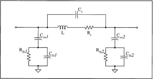
Irrespective of whether these simplifying assumptions can be made, the authors suggest collapsing the resulting concatenation of line segments and corners into a compact circuit model for the purposes of simulation and optimization. A typical compact repre-sentation for an inductor integrated on a silicon substrate8 is exhibited in Figure 2-2, and is similar to that used by Long and Copeland for each segment of a spiral except that all of the intersegment coupling terms are folded into one inductance (lumped together with the self inductance) and one capacitance (appearing as the shunt element Cs). An approxi-mate equivalent circuit based on this network can be fit to the complete model, taking the sums of the individual inductances, resistances, and substrate capacitances as initial esti-mates in the procedure. While this numerical fit does produce a representation more amenable to rapid calculation, any subsequent change in the inductor design necessitates another modeling iteration beginning with the parameter calculations for each segment. This is an unfortunate circumstance in that the optimization of circuits with inductors is itself frequently iterative in nature; trading away some thoroughness in modeling for a simpler procedure may thus be considered a potentially worthwhile exchange.
C,
iCox L RS Cox2
Rsi sil
Rsi2 Csi
2
Figure 2-2. Compact lumped-element model for an inductor on a silicon substrate.
An alternative modeling paradigm is to consider the entire spiral inductor structure and attempt to reason the first-order dependencies that capture its essential characteristics.
8 The shunt legs of the n-network representing the substrate make this model specific to the
sili-con medium. A model for an inductor on a semi-insulating substrate would drop the oxide capacitance term. In addition, the high resistivity of materials such as GaAs and InP makes for negligibly large equivalent substrate resistors, leaving only a capacitance to ground at either end of the network.
Chapter 2: An Approach to Spiral Inductor Modeling
The hope is that this "big picture" approach can yield sufficient accuracy while elimi-nating computational steps between the spiral geometry data and a compact model repre-sentation by focusing on the relevant parasitic effects. A physical model proposed by Yue and Wong [16] adheres to this methodology. In this work the inductance9 is considered laden with three dominant parasitics: series resistance, underpass capacitance, and the effect of the substrate. With the one added assumption that the substrate parasitics are equally distributed (e.g., Co0,=Cox2=Co0 ), the corresponding circuit network is that shown previously in Figure 2-2.
Achieving scalability through physics-based formulations for each of the men-tioned effects is a key element in this work. Taken as geometric parameters in describing the spiral are the width of the conductor that forms the winding (w), the total length of this conductor (1), the number of turns in the winding (N), and the width of the underpass con-ductor (w,,) employed to reach the inner terminal of the spiral. The first parasitic, series resistance, is assumed to originate from the familiar resistivity xlength-area characteristic of imperfect conductors:
RS= , (2.1)
Wteff
where teff represents the effective conductor thickness and is used to model the effects of eddy currents within the conductor. Two sources of these currents-which oppose the applied RF signal-are discussed by Yue and Wong: self induction (from currents within the same trace, also known as the skin effect) and induction via currents flowing in adja-cent traces (proximity effect).10 Enlisting the aid of an electromagnetic field solver to ana-lyze some representative cases, the authors propose that, at 1 GHz and given typical dimensions 1 for interconnect metallization, proximity effects are not significant for uni-planar spirals. Considering then the current distribution in a microstrip line, an equivalent conductor thickness can be derived for use in Equation 2.1:
teff(f) = 6(f)[ - e t(f)]. (2.2)
9 Most of the modeling effort by Yue and Wong, and all of the discussion pertaining to it which
follows, concentrates on the parasitic elements in the spiral model. For the inductance itself, the authors relied upon the Greenhouse method [18], about which more will be said within the con-text of alternative inductance formulations in Section 2.2.1.
10 Ah, the joys Faraday has brought to light. Time-varying magnetic fields induce electric fields in
any material (notwithstanding idealized conductors) through which they pass. Eddy currents thus also flow in the substrate, another mechanism by which Rs can increase.
11 Metal traces with a 20 pm width and 2gm spacing were simulated. To represent the materials
Si02-Chapter 2: An Approach to Spiral Inductor Modeling
In this expression, t represents the physical conductor thickness and 8(f) the skin depth of the conductive material (8(f) oc f 1/2). At 1 GHz, the skin depth of a deposited Al layer is 2.8pm; given a 2gm metal deposition thickness, teff is reduced by nearly 30% (to approximately 1.4gm). This example illustrates that significant increases in the effective series resistance can indeed accrue at frequencies where the skin depth is still appreciably larger than the thickness of the metal.
The next parasitic effect incorporated into this simplified model is the capacitive coupling that shunts portions (or all) of the spiral inductance. As embodied in the approach espoused by Long and Copeland, these coupling terms exist between each pair of segments in a winding. Yue and Wong, however, suggest that these intersegment terms will be small compared to the overlap capacitance between a spiral and its underpass, and that this coupling mechanism can be adequately represented by a single parallel plate capacitor of area NwwUP connected across the series components of the winding:
CS = "".U (2.3)
tox m - m)
The permittivity and thickness of the interlevel dielectric layer separating the "plates"-usually some variant of Si0 2 in Si-based integrated circuits-are denoted EOX and tox(m-m),
respectively. If an inductor were to be constructed with a wide metal winding in a process featuring five or six metal levels, it may be desirable to reduce this capacitance by using an intermediate metal layer (e.g., metal 3 in a five level metal back-end technology) for the underpass rather than the level immediately beneath the spiral. Trade-offs such as this, and the various loss mechanisms in spiral inductors, will be discussed further in Section 2.3.
Each of the remaining parasitic mechanisms instituted by Yue and Wong are owed to the substrate on which the inductor sits. Considering the now-standard Si0 2 on Si
cir-cuit model [14], the authors submit that the oxide capacitance, substrate capacitance, and substrate conductance should all scale with the area occupied by the metallization (1w). Somewhat arbitrarily assuming that the components of this substrate parasitic can be split evenly across the inductor, the final pieces of the simplified model fall into place as:
Bolw
Cox = 2t (,fls ) (2.4)
OX(m - Si)
Csi = (lwCsub)/2, and (2.5)
Chapter 2: An Approach to Spiral Inductor Modeling
Analogous to the formulation for the spiral to underpass capacitance, F-, and tox(m-si) characterize the dielectric between the winding and the surface of the Si substrate. For the substrate itself, Csub and Gsub represent (per unit) area capacitance and conductance terms. Though physical in nature, these terms may essentially be treated as fitting parameters, established empirically through data on measured spirals. This collection of substrate ele-ments completes a simplified yet promising picture of spiral inductors consisting of the most significant parasitic effects and constructed with models that relate the effects to geometry. While this model forms an excellent starting point, a couple of additional developments may offer improvements; these are discussed in Section 2.2.1.
A third tact toward addressing the problem of modeling spiral inductors that has been investigated is the construction of an electromagnetic field solver simplified to the extent possible for handling this one specific case. One such effort by Niknejad and Meyer has resulted in ASITIC12 [17], a tool that combines a set of more computationally-efficient techniques that has been developed for solving EM fields around a metal winding on a multi-layered substrate, with a graphical interface for conveniently generating 2-D spiral layouts of interest. Although the simplifications do appreciably reduce analysis times, the simulations are still too lengthy to provide for efficient inductor optimization. In fact, the procedure used in ASITIC for optimizing a geometry to meet design con-straints still relies upon a collection of approximate lumped-element solutions. This results in a point along the simplicity-accuracy design trade-off that is similar to the other modeling approaches that have been presented.
2.2.1 Alternative Inductance and Series Resistance Formulations
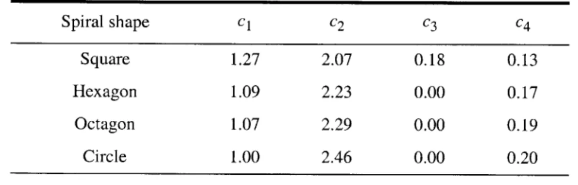
The "divide and conquer" inductor models just described segment the spiral into a conjoined set of straight-line sections for which the self and mutual inductance terms can be calculated (for each section) using Grover's closed-form expressions for rectangular' 3 conductors [13]. The total inductance realized by the spiral can then be computed by summing over all the sections comprising it, a technique generally referred to as the Greenhouse method [18]. While known to yield usable results over a reasonably broad range of geometries, this method is somewhat labor intensive, and becomes difficult to apply to non-rectangular spirals; an expression that could directly provide the inductance with comparable accuracy from simple geometric parameters would be a preferable solution. Several such expressions have been proffered by Mohan, et al. [19], wherein
12 Named more for what it's used rather than for what it is, ASITIC originates from Analysis and Simulation of Inductors and Transformers for Integrated Circuits [17].
![Figure 2- 1. Coupled line segment model proposed by Long and Copeland [ 12].](https://thumb-eu.123doks.com/thumbv2/123doknet/14307758.494911/26.918.146.773.101.446/figure-coupled-line-segment-model-proposed-long-copeland.webp)
![Figure 3-1. Pictorial argument for a time-variant oscillator model, adapted from [34].](https://thumb-eu.123doks.com/thumbv2/123doknet/14307758.494911/45.918.136.767.649.897/figure-pictorial-argument-time-variant-oscillator-model-adapted.webp)