HAL Id: hal-01970254
https://hal.archives-ouvertes.fr/hal-01970254
Submitted on 4 Jan 2019
HAL is a multi-disciplinary open access archive for the deposit and dissemination of sci-entific research documents, whether they are pub-lished or not. The documents may come from teaching and research institutions in France or abroad, or from public or private research centers.
L’archive ouverte pluridisciplinaire HAL, est destinée au dépôt et à la diffusion de documents scientifiques de niveau recherche, publiés ou non, émanant des établissements d’enseignement et de recherche français ou étrangers, des laboratoires publics ou privés.
Non-local signal and noise in T-shape lateral spin-valve
structures
A. Vedyayev, N. Ryzhanova, N. Strelkov, T. Andrianov, A. Lobachev, B.
Dieny
To cite this version:
A. Vedyayev, N. Ryzhanova, N. Strelkov, T. Andrianov, A. Lobachev, et al.. Non-local signal and noise in T-shape lateral spin-valve structures. Physical Review Applied, American Physical Society, 2018, 10. �hal-01970254�
1
Non-local signal and noise in T-shape lateral spin-valve structures
A. Vedyayev1,2, N. Ryzhanova1,2, N. Strelkov1,2, T. Andrianov1, A. Lobachev1 and B. Dieny2 1Department of Physics, Moscow Lomonosov State University, Moscow 119991, Russia 2Univ. Grenoble Alpes, CEA, CNRS, INAC-SPINTEC, 38000 Grenoble, France2
Abstract
The signal and noise in lateral T-shaped spin-valve structures was investigated from a theoretical point of view in diffusive regime. Due to the T shape of the investigated device, It is found that the non-local signal is strongly influenced by the width D of the spin conducting channel, varying substantially on a lateral length-scale of the order of the spin diffusion length 𝑙𝑠𝑓. This effect illustrates the
influence of 2D-dimensionality on spin transport in the spin-channel and in particular the strong impact of not only the device size but also of the device shape on the non-local signal. The non-local signals in the longitudinal and transversal directions of the spin channel were calculated as a function of the angle between the magnetization of the various injecting/collecting magnetic electrodes. In addition, the various sources of noise induced in the lateral spin-valve are discussed with a particular attention on the noise due to the thermally induced fluctuations of the spin accumulation vector in the paramagnetic spin conducting channel. An explicit expression of the dependence of the signal to noise ratio on 𝑙𝑠𝑓 in the paramagnetic spacer and on its dimension was obtained. Implications for the use of such lateral spin-valves as sensors in read-heads for hard disk drives are discussed.
Keywords: Spintronics, lateral spin valves, sensors, read-heads, non-local signal, spin-accumulation, signal to noise ratio
2
Introduction
Spintronic devices rely on the generation, control and detection of spin-polarized current in magnetic nanostructures. Among them, lateral spin-valves are of a particular interest since they allow the manipulation of pure spin currents [1–10]. In these multi-terminal devices, a strong gradient of spin accumulation is generated in a first part of the circuit by flowing a charge current between magnetic electrodes. The gradient of spin accumulation then generates a diffusive spin current, which can propagate in a second part of the device, in directions where no charge current flows. Since the spin is a non-conservative quantity in contrast to the charge, the spin-current spatially decays on a length scale characterized by the spin-diffusion length. Pure spin-current source can then be made to study various spintronic phenomena. Among them, the absorption of spin current can result in a spin transfer torque which may be used to switch the magnetization of magnetic nanostructures [11,12] or excite spin-waves [13] or steady magnetic oscillations [14]. Since the spin current is given by the gradient of spin accumulation, the output signals of lateral spin-valves are all the more important that the spin accumulation itself is maximized at its source. To that respect, it was shown that the introduction of tunnel barriers at the interface between the magnetic electrodes and the spin conducting channel allows optimizing the spin current injection by preventing the back-diffusion of the spin accumulation into the electrodes [15–18]. As a result, part of the spin relaxation is thus suppressed resulting in an enhancement of the spin signal. An additional enhancement can be obtained by laterally confining the spin conducting channel to further reduce the spin relaxation in useless parts of the channel [7].
Here, we investigate a particular two-dimensional geometry of LSV offering an efficient conversion between charge current and spin current [19]. It is sketched in Fig.1. It has a T shape with magnetic layers at each ends of the T. The horizontal top branch of the T comprises two ferromagnetic dots labeled (1) and (3) separated by a paramagnetic spacer (2). The vertical branch of the T is made of a paramagnetic spin conducting channel (4) in contact with the paramagnetic spacer (2) on its top edge and with a third ferromagnetic dots at its bottom edge (5) (Fig. 1). In this model, all parts (1)-(5) are
3 supposed to be in the same plane, have the same thickness and be separated by perfectly flat interfaces.
Fig. 1: Model of the considered lateral spin-valves. 1, 3 and 5 – are ferromagnetic layers (dots). 2 and 4 are paramagnetic layers. The magnetization of layer 3 is fixed along the x-direction. The magnetization of layer 1 can be set along 𝑥 axis (=0) or in the opposite direction (=). The magnetization of layer 5 can take any in- plane (xz) orientation, being the angle between the x-axis and its magnetization. The charge current flows along the 𝑥 x-axis. The output non local voltage is supposed to be measured along the 5-th layer.
As we will show in this paper, the transport along the spin conducting channel cannot be considered here as 1D. The two dimensional character of the spin transport in the channel is important to take into account and yields a significant dependence of the non-local signal not only on the length of the spin conducting channel as well known in the 1D case [17,20,21] but also on its width with a characteristic length scale also of the order of lSF. As a result of this 2D character, the damping of the
spin current as it propagates along the channel is found to be much faster in parallel alignment than in antiparallel alignment of the magnetization in 1 and 3. This effect can be used to increase the sensitivity of the non-local device on the relative orientation of the magnetization in 1 and 3. As a matter of fact, numerical simulations of spin transport in 3D geometry were already performed in Ref. [22] but we provide here an analytical solution. In a second part of the paper, the different sources of noise present in such devices are discussed with a particular focus on the noise due to thermal excitations within the spin accumulation. The signal to noise ratio (SNR) of the device is derived and discussed in comparison to typical SNR values obtained in magnetoresistive readers for hard disk drives. Implication for the use of such lateral spin-valves as readers in hard disk drives are discussed.
Model
4 To start with, the distribution of spin accumulation and profile of induced drop of voltage along the magnetic electrode 5 were calculated for the two-dimensional lateral spin valve structure shown in Fig. 1. We emphasize that we investigate here purely classical effect in diffusive regime associated with the geometry of the investigated device. More explicitly, the injected charge current 𝐽𝑒 flowing
along the 3-2-1 stripe produces a non-equilibrium spin accumulation in conductor 2 which spatially depends on coordinate x. As a result, the spin-current injected from electrode 2 into the paramagnetic channel 4 also depends on coordinate x. We investigated this dependencies for width D of the paramagnetic layer 4 comparable to the spin diffusion length ℓ𝑠𝑓 in paramagnetic layer (ℓ𝑠𝑓≈100
nm). In this range of dimension, quantum size effects which are proportional to the parameter 1/(𝑘𝐹 𝐷) where the Fermi wave vector 𝑘𝐹is of the order of 10 nm-1, are negligible [23]. So our
theoretical approach is based on classical kinetic equation, transformed by Valet and Fert into the system of diffusion equations [24], describing the spin-transport in spin-valves in CPP geometry. Because quantum confinement effects are expected to be negligible in the investigated device, we did not use the non-equilibrium Green function approach presented in Ref. [25] but rather the classical diffusive approach. Besides, it was shown that the non-equilibrium Green function approach, after some reasonable approximations, leads to the same diffusion equations, suggested in Ref. [24] in the case of collinear orientation of magnetizations of ferromagnetic layers in magnetic multilayers.
Electrical 𝑗⃗𝑒 and spin 𝑗̂𝑚 currents in spin-diffusion theory can be written in each layer as:
𝑗𝑒𝑖 = −𝜎 𝜕 𝜕𝜉𝑖𝜑 − 𝛽 𝜎 𝜈∑ 𝑀𝑗 𝜕 𝜕𝜉𝑖𝑚𝑗 𝑗 , 𝑗𝑚𝑖𝑗 = −𝜎𝛽𝑀𝑗 𝜕 𝜕𝜉𝑖𝜑 − 𝜎 𝜈 𝜕 𝜕𝜉𝑖𝑚𝑗, (1)
where 𝜉𝑖 – is the coordinate axis, 𝜎 –the conductivity of the layer, 𝛽 – spin asymmetry parameter of
the conductivity, 𝜑 –the electrical potential, 𝜈 –the electron density of states at Fermi energy, 𝑀⃗⃗⃗ – unit vector along magnetization of the layer, 𝑚⃗⃗⃗ – spin accumulation vector. We adopted the electron charge 𝑒 = 1. The diffusion equations are written:
∑ 𝜕 𝜕𝜉𝑖 𝑗𝑒𝑖 = 0, ∑ 𝜕 𝜕𝜉𝑖𝑗𝑚 𝑖𝑗 𝑗 = 𝑚𝑗 𝜏𝑠𝑓, 𝑖 (2)
5 The independent variables 𝜑 and 𝑚⃗⃗⃗ depend on two coordinates 𝜉𝑖 = 𝑥, 𝑧. In this case, assuming
the condition of zero electrical and spin currents perpendicular to the lateral sides of 4-th and 5-th layers, the solutions of equations (2) for spin accumulation and potential in 4-th and 5-th layers can be written as:
𝑚 = ∑[(𝑎 sin 𝜘𝑥 + 𝑏 cos 𝜘𝑥)𝑒−𝑘𝑧+ (𝑎′ sin 𝜘𝑥+ 𝑏′ cos 𝜘𝑥)𝑒𝑘𝑧] 𝜘
,
𝜑 = ∑[(𝑐 sin 𝜆𝑥 + 𝑑 cos 𝜆𝑥)𝑒−𝜆𝑧+ (𝑐′ sin 𝜆𝑥 + 𝑑′ cos 𝜆𝑥)𝑒𝜆𝑧] − 𝛽𝑚
𝜈
𝜆
,
(3)
where 𝑘2= 1/𝑙2+ 𝜘2, 𝑙 – is the spin diffusion length in the corresponding layer, 𝜘 = 𝜆 = 𝜋𝑛/𝐷, 𝑛 = 0, 1, …. The unknown coefficients can be found from the conditions of continuity of all currents. The solutions for the potential 𝜑 in layer 5 is then:
𝜑5= ∑ 𝑚̃2𝑛 𝔇 𝑛 [cosh 𝜋𝑛 𝐷 (𝐿5− 𝑧) sinh𝜋𝑛𝐷 (𝐿5− 𝐿4) 𝜎42𝑘 4𝛽5 𝜈4𝜈5𝜎5 cosh 𝜋𝑛 𝐷 𝐿4 − cosh 𝑘5(𝐿5− 𝑧) cosh 𝑘5(𝐿5− 𝐿4) 𝜎4𝑘4𝛽5 𝜈4𝜈5 (sinh 𝜋𝑛 𝐷 𝐿4 +𝜎4 𝜎5coth 𝜋𝑛 𝐷 (𝐿5− 𝐿4) cosh 𝜋𝑛 𝐷 𝐿4)] cos 𝜋𝑛 𝐷 𝑥 , (4) 𝑚̃2𝑛= 2 𝐷 ∫ 𝑚2(𝑥) cos 𝜋𝑛 𝐷 𝑥 𝑑𝑥 0 −𝐷 , with 𝔇 = cosh𝜋𝑛 𝐷 𝐿4[ 𝛽52𝜎 4 𝜈5 𝜋𝑛 𝐷 sin 𝑘4𝐿4+ 𝜎42𝑘 4 𝜎5𝜈4cosh 𝑘4𝐿4coth 𝜋𝑛 𝐷 (𝐿5− 𝐿4) +1 − 𝛽52 𝜈5 𝑘5𝜎4sinh 𝑘4𝐿4coth 𝜋𝑛 𝐷 (𝐿5− 𝐿4) tanh 𝑘5(𝐿5− 𝐿4)] + sinh𝜋𝑛 𝐷 𝐿4[ 1 − 𝛽52 𝜈5 𝑘5𝜎5sinh 𝑘4𝐿4tanh 𝑘5(𝐿5− 𝐿4) + 𝜎4𝑘4 𝜈4 cosh 𝑘4𝐿4] , (5)
where 𝑚2(𝑥) – is the profile of spin accumulation in layer 2. In expressions (4), we kept terms
depending on the mutual orientations of magnetizations in ferromagnetic electrodes: if signs of all 𝛽𝑖
are equal, the magnetizations of all electrodes are parallel and if one sign is opposite to the two others, the magnetization of this electrode is antiparallel to the two other ones.
6
To give some insights into the physical meaning of expression (4), we rewrote it in the case n=0 (lowest order in Fourier expansion) and under the conditions σ4 ≫ σ5, L4/ℓ4≫ 1:
𝜑5 = 𝜑̃2(0)+ 𝑚̃2(0)2𝛽5 𝜈5 (1 − cosh(𝐿5− 𝑧)/ℓ5 cosh(𝐿5− 𝐿4)/ℓ5) 𝑒 −𝐿4/ℓ4 ≡ const −𝛽5 𝜈5𝑚5, 𝜑̃2(0)= 2 𝐷∫ 𝜑2(𝑥) 𝑑𝑥 0 −𝐷 . (6)
So if 𝑚̃2𝑛=0 for 𝑛 > 0 (which is the case for very narrow channel 4 for instance i.e. D<<ℓ𝑠𝑓), the
potential in the paramagnetic layer 4 is found to be uniform (independent on coordinates z and x), while it depends on z in the ferromagnetic layer 5 (analyzer) as described by relation (6). Actually a linear relationship of the form 𝜑 = 𝜑0− 𝛽𝑚/𝜈 exists in conductor 5 between the local potential and
the local spin accumulation. If higher orders in Fourier expansion are taken into account, the potential and spin accumulation are everywhere non-uniform, as will be shown later.
7
Fig. 2: Profile of spin accumulation 𝑚4 in layer 4 along x axis for parallel and antiparallel orientation of magnetizations in electrodes 1 and 3 and for three values of coordinate 𝑧. Magnetization in 5 is supposed to be oriented along x-axis direction (5=0.7). The origin (x=0, z=0) is at the bottom right
corner of conductor 2 in Fig.1. Point 𝑧 = +400𝑛𝑚 corresponds to the interface between 4 and 5 layers. Units of 𝑚4 is the difference between the numbers of accumulated electrons per atom with spin “up” and spin “down”. Parameters are: 𝜎1= 𝜎3= 𝜎5= 0.001 (𝛺 ⋅ 𝑛𝑚)−1, 𝜎2= 𝜎4= 0.01
(𝛺 ⋅ 𝑛𝑚)−1, ℓ1= ℓ
3= ℓ5= 10𝑛𝑚, ℓ2= ℓ4= 100𝑛𝑚, 𝜈 = 0.1, 𝛽1= 0.7, 𝐿 = 400𝑛𝑚, 𝐿4=
400𝑛𝑚, 𝐿5= 500𝑛𝑚, applied voltage 𝑉 = 1𝑉𝑜𝑙𝑡.
In Fig. 2, the profile of spin accumulation along x direction for different values of coordinate z is shown for parallel and antiparallel orientation of the magnetization in layers 1 and 3. In the case of antiparallel configuration (AP) between magnetization in layer 1 and 3 (upper graph in Fig.2), the spin accumulation in conductor 2 between 1 and 3 takes a large value, weakly dependent on x in conductor 2 and exhibiting an even symmetry with respect to the vertical symmetry plane of the device (plane x=-150nm for the chosen geometry). At position z=+300nm along the spin conducting channel, this even symmetry is still reminiscent. At position z=+350nm and z=+400nm, the spin accumulation distribution gets more and more affected by the magnetic conductor 5 whose magnetization points
8 along x explaining the rising asymmetry observed on the curves for these positions. If we now look at the drop of the maximum value of the spin accumulation (value at x=-300nm) between z=+300nm and z=+400nm, the drop is by a factor ~2 in this case of AP configuration between 1 and 3.
In contrast, in the situation of parallel configuration (P) between the magnetization in 1 and 3, the profile of spin accumulation in 2 has an odd shape with respect to the plane of symmetry (x=-150nm) varying from a large positive value at the interface with 1 to a large negative value at the interface with 3. At z=+300nm, +350nm and +400nm, this odd profile remains. However, the maximum values of spin accumulation (value at x=-300nm) on this profile drops at a much faster rate in this P configuration than in the previous AP configuration. Indeed, between z=+300nm and z=+400nm, the drop is by a factor ~7 in the P case whereas it is ~2 in the AP case. This demonstrates that the stronger transversal gradient (in x-direction) of spin accumulation present in the P case is more strongly attenuated in its diffusion along the spin channel in the z direction than the shallower gradient present in the AP case.
In the used geometry, this difference in spin current attenuation and the resulting drop of voltage 𝛥𝜑 measured across the ferromagnetic layer 5 strongly depends on the width of the spin conducting channel as illustrated in Fig.3 and Fig. 4. These figures show the profiles of the drop of voltage along 𝑧 axis in ferromagnetic layer 5 for two different widths of the spin conducting channel (Fig.3: Narrow spin channel D=100nm; Fig.4: Wide spin channel D=300nm).
When the magnetizations of the two ferromagnetic electrodes 1 and 3 are assumed to be parallel, the spin accumulation in layer 2 is an antisymmetric function of coordinate 𝑥, so 𝑚̃20 = 0 and the main
contribution into the drop of voltage is due to the first harmonic in (3).
For the narrow spin channel 4 and in parallel case (Fig.3a), the spin accumulation decreases sharply exponentially along the 𝑧-axis in layer 4. The spin current has almost vanished when reaching the ferromagnetic layer 5 so that the value of the drop of voltage 𝛥𝜑 is quite small (𝛥𝜑 = 0.32 10−7Volt)
for the parameters listed in the caption of Fig. 2.
In the case of wide spin channel (Fig. 4a), the spin accumulation decreases much more slowly so that the drop of voltage 𝛥𝜑 increases up to 10−4 for an applied bias voltage of 1V. In both cases, the drops
9 of potential measured on the opposite sides of ferromagnetic electrode 5 at 𝑥 = 0 and 𝑥 = −𝐷 have opposite sign. This feature is reminiscent of the antisymmetry of the spin accumulation built up in conductor 2. Due to this antisymmetry, a transverse drop of voltage 𝛿 = 𝜑|𝑥=0− 𝜑|𝑥=−𝐷 could also
be measured across the ferromagnetic layer 5 similar to a quasi Hall effect. This transverse Hall voltage is small (𝛿~0.7 10−6𝑉 at z=400nm) for the narrow spin channel, due to the almost complete attenuation of the spin current along the spin conducting channel. It is however significant in the case of the wide channel since the spin current attenuation is then much weaker (𝛿~0.27 10−3𝑉 at z=400nm).
Concerning the amplitude of the longitudinal drop of voltage across the ferromagnetic layer 5, Δ𝜑 weakly varies in absolute value as a function of the orientation of the magnetization of 5 with respect to 1 and 3. Indeed, in the narrow spin channel case, Δ𝜑 is in any case very small so that its variation as the magnetization of 5 is reversed (i.e. 5 changes sign) is even smaller (<10-7V). In the case of wide
spin channel, this variation is larger but still fairly small Δ𝜑𝛽5=0.7− Δ𝜑𝛽5=−0.7= 0.06 10
−4𝑉 at
10 -4 -2 0 2 4
b)
3.11 x 10⁻⁷
5-0.5 (V)
5= 0.7, x=0 5= 0.7, x=-100 5= -0.7, x=0 5= -0.7, x=-100 x10-7 3.43 x 10⁻⁷a)
400 420 440 460 480 500 -0.4 0.0 0.4 0.64 x 10-4 x10-4
5-0.5 (V)
z (nm)
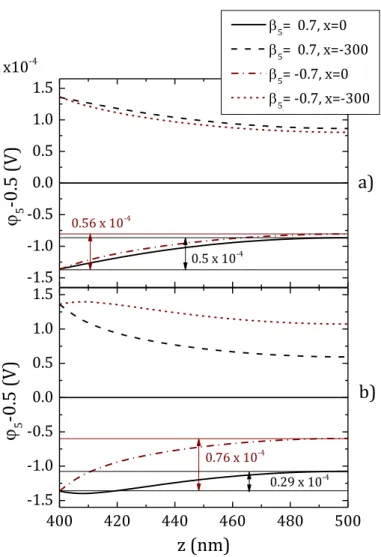
Fig. 3: Potential profile along the two lateral sides (x=0 and x=-100nm) of the ferromagnetic layer 5 in the case of a narrow spin channel (𝐷 = 100nm) as a function of position along z-axis in case of (a) parallel configuration between 1 and 3 (𝛽3= 0.7) and (b) antiparallel configuration
between 1 and 3 (𝛽3= −0.7). In each graph, two situations are considered: The magnetization of ferromagnet 5 is either assumed to point along the positive x-axis for 5=0.7 or along the
negative x-axis for 5=-0.7. 𝜎1= 𝜎3= 𝜎5= 0.001 (𝛺 ⋅ 𝑛𝑚)−1, 𝜎2= 𝜎4= 0.01 (𝛺 ⋅ 𝑛𝑚)−1, ℓ1=
ℓ3= ℓ5= 10𝑛𝑚, ℓ2= ℓ4= 100𝑛𝑚, 𝜈 = 0.1, 𝛽1= 0.7, 𝐿 = 400𝑛𝑚, 𝐿4= 400𝑛𝑚, 𝐿5=
500𝑛𝑚, applied bias voltage 𝑉 = 1𝑉𝑜𝑙𝑡. The numbers in the graph indicate the amplitude of the
11 -1.5 -1.0 -0.5 0.0 0.5 1.0 1.5 x10⁻⁴ 5= 0.7, x=0 5= 0.7, x=-300 5= -0.7, x=0 5= -0.7, x=-300 0.56 x 10⁻⁴ 0.5 x 10⁻⁴
5-0.5 (V)
a)
b)
400 420 440 460 480 500 -1.5 -1.0 -0.5 0.0 0.5 1.0 1.5 0.29 x 10⁻⁴ 0.76 x 10⁻⁴
5-0.5 (V)
z (nm)
Fig. 4: Potential profile along the two lateral sides (x=0 and x=-300nm) of ferromagnetic layer 5 in the case of a wide spin channel (𝐷 = 300nm) as a function of position along z-axis in case of (a) parallel configuration between 1 and 3 (𝛽3= 0.7) and (b) antiparallel configuration between 1 and 3 (𝛽3= −0.7). In each graph, two situations are considered: The magnetization of ferromagnet 5 is either assumed to point along the positive x-axis for 5=0.7 or along the negative
x-axis for 5=-0.7. Other parameters are the same as in Fig.3.
In the case of antiparallel orientation of magnetizations of ferromagnetic electrodes 1 and 3, the spin accumulation in conductor 2 has a symmetric profile with a large average value. As previously discussed the attenuation of the spin current during its propagation along the spin conducting channel is weaker than in the parallel case resulting in larger signals Δ𝜑 across the ferromagnetic layer 5.
In the case of the narrow spin channel (𝐷 = 100nm), the value of 𝑚̃21= 0 and the main contribution
12 accumulation in conductor 2). The drop of voltage Δ𝜑 across the ferromagnetic layer 5 is much larger than in the parallel case, reaching 0.64 10-4V. This value changes sign when the magnetization of 5 is
reversed yielding a total variation of voltage of 1.28 10-4V upon magnetization reversal. In addition,
the profiles of the potential variation 𝜑5(𝑧) along the two sides of the ferromagnetic layer 5 are the
same (Fig.3b, same curves for x=0 and x=-100nm for the same value of 5). This means that no
transverse voltage would be measured in this case in contrast to the situation where 1 and 3 are in parallel configuration. This is due to the even symmetry of the spin accumulation built up in conductor 2 in this antiparallel configuration of 1 and 3.
For the wide spin channel (Fig.4), 𝑚̃21 is still zero, but some contributions in 𝜑5(𝑧) yield terms
proportional to: 𝜑̃21= 1 𝐷 ∫ 𝜑(𝑥) cos 𝜋𝑥 𝐷 𝑑𝑥 0 −𝐷 , (7)
omitted in (4) for simplicity. In this case, the distribution of potential over the ferromagnetic layer 5 has a more complex behavior shown in Fig.5 in the case where the magnetization in 5 is pointing along the +x-axis. This asymmetric distribution yields drops of voltage both in the longitudinal (along z-axis) and transverse (along x-axis) directions. These drops of voltages also significantly depends on the magnetization orientation in ferromagnetic layer 5 as shown in Fig.4b. For instance, at x=0, the drop of voltage Δ𝜑 across the ferromagnetic layer 5 varies from 0.29 10-4V to 0.76 10-4V upon reversing the
magnetization in layer 5.
Interestingly, in the antiparallel configuration of 1 and 3, the variation of Δ𝜑 across the ferromagnetic layer 5 upon rotating the magnetization of ferromagnetic layer 5 can be the basis of a magnetic field sensor. The layers 1 and 3 would be pinned whereas the ferromagnetic layer 5 would constitute the sense layer of the sensor. Both narrow and wide spin channel could be used since Δ𝜑 significantly varies when 5 changes sign as illustrated in Fig.3b and 4b.
13
Fig. 5: Distribution map of potential 𝜑5 in the ferromagnetic layer 5 for antiparallel configuration of the magnetization in 1 and 3. The parameters are the same as in Fig. 2. Magnetization in 5 is supposed to be oriented along x-axis direction
For sensor applications, linearity of the response is important. The angular dependence of the signal Δ𝜑 = 𝜑|𝑧=𝐿4− 𝜑|𝑧=𝐿5 on the angle between magnetisations of the ferromagnetic electrodes 1 or 5 was therefore investigated. Fig.6 shows this dependence as a function of the cosine of the angle between the magnetization in 1 and 5. A (1 − cos 𝜃) variation is found in the narrow spin channel case and a 𝑐𝑜𝑛𝑠𝑡 + (1 − cos 𝜃) for the wide spin channel case due to the contribution into the signal from the above mentioned terms proportional to 𝜑̃21.
14
-1.0
-0.5
0.0
0.5
1.0
-1.0
-0.5
0.0
0.5
1.0
x10
-4 D=300nm D=100nm
(V)
cos
Fig. 6: Dependence of 𝛥𝜑 at 𝑥 = −𝐷 on the angle 𝜃 between magnetization of layer 5 and x-axis for narrow (solid line) and wide (dashed line) spin channel for AP configuration between 1 and 3. Other parameters are the same as in Fig.3.
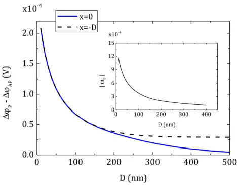
The signal amplitude Δ𝜑0°− Δ𝜑180° associated with a 180° full rotation of the magnetization of
the sense layer 5 was calculated as a function of the spin channel width. The calculation was carried out at both edges of layer 5 (x=0 and x=-D) and the results are shown in Fig. 7. It is clear that for narrow spin channels ( 𝐷 < 1.5 ⋅ 𝑙2), the curves at both edges coincide and the main contribution arises from
the zeroth order component of the Fourier expansion for 𝑚2, which depends on 𝐷 as shown in the
inset of Fig. 7. For wider spin channel, these curves no longer coincide as the contribution of 1st
15 0 100 200 300 400 500 0.0 0.5 1.0 1.5 2.0 x10⁻⁴
P-
AP(V)
D (nm) x=0 x=-D 0 100 200 300 400 0 3 6 9 12 15 x10-4 | m 0 | D (nm)Fig. 7: Dependence of the effect 𝛥𝜑𝑃− 𝛥𝜑𝐴𝑃 on the width of paramagnetic layer 𝐷 at 𝑥 = 0 and
𝑥 = −𝐷 for 𝛽 = 0.7. Other parameters are the same as in Fig.3.
Besides the signal itself, an important characteristic to investigate for sensor application is the noise and the resulting signal to noise ratio. Different mechanisms of noise in mesoscopic systems with ferromagnetic electrodes were investigated in earlier studies [26–29]. We evaluate here the signal to noise ratio (SNR) in the present lateral structure. The SNR is defined as Δ𝜑0/√𝛿〈(Δ𝜑)2〉,
where 𝛿〈(Δ𝜑)2〉 is the mean quadratic deviation of the signal.
A first source of noise is the Johnson noise √4𝑘𝐵𝑇𝑅∆𝑓 . Assuming a bandwidth of 2GHz, a sheet
resistance (resistivity/thickness) of the element 50, the Johnson noise amplitude is estimated to be of the order of 20V. Considering that the expected signal is typically of the order of 100V (see Fig.7),
this means Δ𝜑
√𝛿〈(Δ𝜑)2〉𝐽𝑜ℎ𝑛𝑠𝑜𝑛~5
Another source of noise may be associated with fluctuations of the direction of magnetizations of the ferromagnetic sense electrode 5. It is easy to show following Ref. [30] that:
16 Δ𝜑 √𝛿〈(Δ𝜑)2〉 𝑚𝑎𝑔.𝑓𝑙𝑢𝑐𝑡. = 1 |sin 𝜃|√8 𝐾𝐹Ω 𝑘𝐵𝑇 , (8)
where 𝐾𝐹 is the uniaxial anisotropy constant, Ω – volume of the soft ferromagnetic electrode
(element 5 in Fig.1), 𝑇 – temperature, 𝜃 – the angle between the magnetization of ferromagnetic electrode 5 and x-axis. Assuming an anisotropy 𝐾𝐹= 5.103𝐽/𝑚3, a volume of the magnetic dot 5 of
3nm*100nm*100nm, (7) yields Δ𝜑
√𝛿〈(Δ𝜑)2〉𝑚𝑎𝑔.𝑓𝑙𝑢𝑐𝑡.~17 around 𝜃 = 90°.
Besides, another source of noise in the investigated lateral spin-valves may originate from the thermally induced fluctuations of the spin accumulation 𝑚2(0) in the paramagnetic layers 2 and 4. In
this case: Δ𝜑 √𝛿〈(Δ𝜑)2〉= 1 |sin 𝜃|√ |𝑚| 2𝑘𝐵𝑇𝜒′ , (9)
where 𝜒′ is the real part of the static susceptibility of the spin accumulation. The latter can be calculated by adding the term 𝛾[𝑚⃗⃗⃗ × 𝐻⃗⃗⃗] in equations (1), (2), where H – is a small fluctuating magnetic field in the 𝑧-direction.
Linearizing and solving this system of equations to first order in 𝐻0𝑧 yields the explicit expression
of the static susceptibility and finally the SNR expression:
Δ𝜑 √𝛿〈(Δ𝜑)2〉 𝑓𝑙𝑢𝑐𝑡 ∆𝜇 = |𝑚2 (0)| |sin 𝜃|[ 𝑘𝐵𝑇 ℏ𝑁eff𝔇𝐷 ∫ 𝑑𝑥 |𝐶1𝑒 𝑥 𝑙2+ 𝐶2𝑒−𝑥𝑙2| 0 −𝐷 ] −12 , (10)
where 𝑁eff= 𝑙2𝐷𝑡/𝑎03, 𝑡 is the thickness of the paramagnetic layer in 𝑦-direction, 𝑎0 - the lattice
17 𝑚2(0)= 1 𝐷 ∫ (𝑎2𝑒 −𝑥𝑙 2+ 𝑏2𝑒 𝑥 𝑙2) 𝑑𝑥 0 −𝐷 , 𝑎2 = 𝑒𝑉𝜈𝛽 4𝐿ℜ [ 1 𝑙2(1 + 𝑒 −𝐷𝑙 2) +𝜎(1 − 𝛽 2) 𝜎2𝑙 (1 − 𝑒 −𝐷𝑙 2)], 𝑏2=𝑒𝑉𝜈𝛽 4𝐿ℜ [ 1 𝑙2(1 + 𝑒 𝐷 𝑙2) +𝜎(1 − 𝛽 2) 𝜎2𝑙 (1 − 𝑒 𝐷 𝑙2)], ℜ = cosh𝐷 𝑙2 1 − 𝛽2 𝑙2𝑙 + sinh 𝐷 𝑙2( 𝜎2 𝜎 1 𝑙22+ 𝜎 𝜎2 (1 − 𝛽2)2 𝑙2 ), 𝐶1=1 2 Im 𝑘1𝑙22[𝑏 2𝑙2sinh𝐷𝑙 2+ 𝑎2𝐷𝑒 𝐷 𝑙2] 2𝑙2Re 𝑘1cosh𝑙𝐷 2+ (𝑙2 2|𝑘 1|2+𝜎𝜎 ) sinh2 𝐷𝑙 2 , 𝐶2= −1 2 Im 𝑘1𝑙22[𝑎 2𝑙2sinh𝐷𝑙 2+ 𝑏2𝐷𝑒 −𝐷𝑙 2] 2𝑙2Re 𝑘1cosh𝐷𝑙 2+ (𝑙2 2|𝑘 1|2𝜎𝜎 2+ 𝜎2 𝜎 ) sinh𝐷𝑙2 , 𝑘1= √𝑙1 2 2+ 𝑖
𝑙𝑝𝑟2 , where 𝑙𝑝𝑟 – spin-precession length in the ferromagnetic layer [31], 𝜎 = 𝜎1= 𝜎3, 𝑙1= 𝑙3= 𝑙 and 𝛽 = 𝛽1= −𝛽3 (antiparallel configuration between 1 and 3).
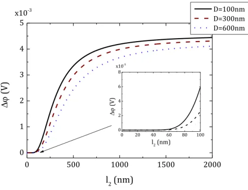
18 0 500 1000 1500 2000 0 1 2 3 4 5 x10⁻³ D=100nm D=300nm D=600nm
(V)
l
2(nm)
0 20 40 60 80 100 0 2 4 6 8 (V) l2 (nm) x10-5Fig. 8: Signal dependence versus 𝑙2 (spin diffusion length) for different values of 𝐷. Other parameters are the same as in Fig.3. The inset is a zoom on the more realistic region of low 𝑙2 values (Up to 100nm). 0 500 1000 1500 2000 0.0 0.4 0.8 1.2 1.6 0.0 0.6 1.2 1.8 2.5 x10⁻⁴
(
)|
t=8 0nm·|sin
| (V)
lpr=0.5 lpr=1 lpr=5(
)|
t=2 nm·|sin
| (V)
l
2(nm)
x10-5Fig.9: Dependence of noise due to fluctuations in spin accumulation versus 𝑙2 (spin diffusion length) for different values of 𝑙𝑝𝑟 and for two values of the thickness 𝑡 of the structure (t=2nm, left vertical scale and t=80nm, right vertical scale). Other parameters are the same as in Fig.3.
19
0
250
500
750
1000
0
20
40
60
0
125
250
375
SN
R|
t=8 0nm·|sin
|
lpr=0.5 lpr=1 lpr=5SN
R|
t=2 nm·|sin
|
l
2(nm)
0 2 4 6 8 10 2 4 6 8 12.5 25.0 37.5 50.0 SNR | t=8 0nm ·|s in | SNR |t=2 nm ·|s in | l2 (nm)Fig. 10: Ratio of Signal/Noise due to thermal fluctuations of spin accumulation (SNR) dependence versus 𝑙2 (spin diffusion length) for different values of 𝑙𝑝𝑟 and for two values of the thickness 𝑡 of the structure (t=2nm, left vertical scale and t=80nm, right vertical scale). Other parameters are the same as in Fig.3
Both signal and noise increase and saturate with increasing 𝑙2 due to exponential attenuation of
the spin accumulation travelling along the spin channel 4 (see Fig. 1). They saturate for values of 𝑙2
larger than the spin channel length. Meanwhile in the expression of the signal to noise ratio (SNR) associated with thermal fluctuations of spin accumulation, these exponents cancel so that for small values of 𝑙2 the dependence of SNR is of the form 𝐶0+ 𝐶1𝑙2 as shown in the inset of Fig. 10. Concerning
the dependence of noise and SNR versus 𝑙𝑝𝑟 (Fig.9 and 10), it is observed that shorter 𝑙𝑝𝑟 yields lower
noise and larger SNR. Shorter 𝑙𝑝𝑟 in the ferromagnetic layers actually means stronger exchange
interactions in the ferromagnetic electrodes which can reinforce the orientation and stiffness of the spin accumulation in the paramagnetic spacer, so reducing its fluctuations.
The comparison of the 3 sources of noise discussed above yields SNRJohnson~3 to 10 depending on
20 dot 5 (in particular its anisotropy energy), SNRfluct ~10-50 depending mostly on the properties of the
spin conducting channel (in particular the susceptibility of the spin accumulation), it seems that the dominant one is the Johnson noise due to the relative weakness of the non-local output signal. Adding the 3 sources of noise together yields a net SNR given by : 𝑆𝑁𝑅1 =𝑆𝑁𝑅 1
𝐽𝑜ℎ𝑛𝑠𝑜𝑛+
1 𝑆𝑁𝑅𝑀𝑎𝑔 𝑓𝑙𝑢𝑐𝑡+
1 𝑆𝑁𝑅fluct ∆μ. This means a net SNR in the range between ~2 and ~6. Using the convention SNR=20log10(signal
amplitude/noise amplitude), this yields SNR values in the range 6dB to 16dB.
This type of lateral spin-valve sensors could a priori be interesting to use as magnetic field sensors in hard disk drives. There, the magnetic dot 5 would serve as a sense layer and be inserted in the read gap of the head next to the air bearing surface (ABS). The advantage of using such lateral spin-valves as read-head rather than a magnetic tunnel junction (MTJ) is the total thickness of the device. This thickness has to be as small as possible since it determines the shield to shield spacing which directly influences the downtrack spatial resolution. Since 1991 where the first magnetoresistive heads were introduced based on anisotropic magnetoresistance (AMR) [32], several technologies of magnetoresistive heads have been developed [32] successively based on the current in-plane giant magnetoresistance (CIP-GMR) of spin-valves [33] and on tunnel magnetoresistance (TMR) [34]. Nowadays, a conventional MgO-based in-plane magnetized MTJ for hard disk drive has a typical thickness of the order of 22nm. In contrast, lateral spin-valves with additional insulating bottom and top layer could have a total thickness of about 14nm or even less compatible with the requirement for areal density of 5Tbit/in² [35]. However, at the moment, the SNR calculated above for the investigated lateral spin-valves (6dB-16db) is much lower than in conventional sensors based on tunnel magnetoresistance or current perpendicular to plane giant magnetoresistance (SNR in the range 30-40dB) [36]. It is therefore important to further increase the output signal in these lateral spin valves to fully exploit the advantage of their reduced thickness for read-heads used in hard disk drives.
21 Acknowledgements: This work was partially funded by the ERC Adv grant MAGICAL n°669204.
22
References
[1] T. Kimura and Y. Otani, Phys. Rev. Lett. 99, 196604 (2007).
[2] T. Kimura and Y. Otani, J. Phys. Condens. Matter 19, 165216 (2007). [3] T. Kimura, T. Sato, and Y. Otani, Phys. Rev. Lett. 100, (2008).
[4] E. Villamor, M. Isasa, L. E. Hueso, and F. Casanova, Phys. Rev. B 87, 94417 (2013). [5] H. Idzuchi, Y. Fukuma, and Y. Otani, Sci. Rep. 2, 628 (2012).
[6] E. Villamor, M. Isasa, L. E. Hueso, and F. Casanova, Phys. Rev. B 88, 184411 (2013). [7] P. Laczkowski, L. Vila, V.-D. Nguyen, A. Marty, J.-P. Attané, H. Jaffrès, J.-M. George, and A.
Fert, Phys. Rev. B 85, 220404 (2012).
[8] W. Savero Torres, P. Laczkowski, V. D. Nguyen, J. C. Rojas Sanchez, L. Vila, A. Marty, M. Jamet, and J. P. Attané, Nano Lett. 14, 4016 (2014).
[9] V. T. Pham, L. Vila, G. Zahnd, A. Marty, W. Savero-Torres, M. Jamet, and J.-P. Attané, Nano Lett. 16, 6755 (2016).
[10] G. Zahnd, L. Vila, V. T. Pham, A. Marty, C. Beigné, C. Vergnaud, and J. P. Attané, Sci. Rep. 7, 9553 (2017).
[11] L. Liu, C.-F. Pai, Y. Li, H. W. Tseng, D. C. Ralph, and R. A. Buhrman, Science (80-. ). 336, 555 (2012).
[12] T. Yang, T. Kimura, and Y. Otani, Nat. Phys. 4, 851 (2008).
[13] Y. Kajiwara, K. Harii, S. Takahashi, J. Ohe, K. Uchida, M. Mizuguchi, H. Umezawa, H. Kawai, K. Ando, K. Takanashi, S. Maekawa, and E. Saitoh, Nature 464, 262 (2010).
[14] L. Liu, T. Moriyama, D. C. Ralph, and R. A. Buhrman, Phys. Rev. Lett. 106, 36601 (2011). [15] Y. Fukuma, L. Wang, H. Idzuchi, and Y. Otani, Appl. Phys. Lett. 97, 12507 (2010). [16] T. Wakamura, K. Ohnishi, Y. Niimi, and Y. Otani, Appl. Phys. Express 4, 63002 (2011). [17] Y. Fukuma, L. Wang, H. Idzuchi, S. Takahashi, S. Maekawa, and Y. Otani, Nat Mater 10, 527
(2011).
[18] H. Jaffrès, J.-M. George, and A. Fert, Phys. Rev. B 82, 140408 (2010).
[19] T. Andrianov, A. Vedyaev, and B. Dieny, J. Phys. D Appl. Phys. 51, 205003 (2018). [20] S. Nonoguchi, T. Nomura, and T. Kimura, Appl. Phys. Lett. 100, (2012).
[21] Ikhtiar, S. Kasai, A. Itoh, Y. K. Takahashi, T. Ohkubo, S. Mitani, and K. Hono, J. Appl. Phys. 115, (2014).
[22] S. Takahashi and S. Maekawa, Phys. Rev. B 67, 52409 (2003).
[23] A. Vedyayev, C. Cowache, N. Ryzhanova, and B. Dieny, J. Phys. Condens. Matter 5, 8289 (1993).
23 [25] C. O. Pauyac, M. Chshiev, A. Manchon, and S. A. Nikolaev, Phys. Rev. Lett. 120, 176802
(2018).
[26] Y. Tserkovnyak and A. Brataas, Phys. Rev. B 64, 214402 (2001).
[27] J. Foros, A. Brataas, G. E. W. Bauer, and Y. Tserkovnyak, Phys. Rev. B 75, 92405 (2007). [28] T. Szczepański, V. K. Dugaev, J. Barnaś, J. P. Cascales, and F. G. Aliev, Phys. Rev. B 87, 155406
(2013).
[29] T. Arakawa, J. Shiogai, M. Ciorga, M. Utz, D. Schuh, M. Kohda, J. Nitta, D. Bougeard, D. Weiss, T. Ono, and K. Kobayashi, Phys. Rev. Lett. 114, 16601 (2015).
[30] A. A. Smits, Tunnel Junctions : Noise and Barrier Characterization (Eindhoven : Technische Universiteit Eindhoven, 2001).
[31] S. Zhang, P. M. Levy, and A. Fert, Phys. Rev. Lett. 88, 236601 (2002). [32] E. E. Fullerton and J. R. Childress, Proc. IEEE 104, 1787 (n.d.).
[33] B. Dieny, V. S. Speriosu, S. Metin, S. S. P. Parkin, B. A. Gurney, P. Baumgart, and D. R. Wilhoit, J. Appl. Phys. 69, 4774 (1991).
[34] J.-G. (Jimmy) Zhu and C. Park, Mater. Today 9, 36 (2006).
[35] Y. K. Takahashi, S. Kasai, S. Hirayama, S. Mitani, and K. Hono, Appl. Phys. Lett. 100, 52405 (2012).
[36] G. Mihajlović, J. C. Read, N. Smith, P. van der Heijden, C. H. Tsang, and J. R. Childress, IEEE Magn. Lett. 8, 1 (2017).