HAL Id: tel-03137598
https://tel.archives-ouvertes.fr/tel-03137598
Submitted on 10 Feb 2021
HAL is a multi-disciplinary open access
archive for the deposit and dissemination of
sci-entific research documents, whether they are
pub-lished or not. The documents may come from
teaching and research institutions in France or
abroad, or from public or private research centers.
L’archive ouverte pluridisciplinaire HAL, est
destinée au dépôt et à la diffusion de documents
scientifiques de niveau recherche, publiés ou non,
émanant des établissements d’enseignement et de
recherche français ou étrangers, des laboratoires
publics ou privés.
A theoretical study of correlation effects of N electrons
in semiconductor nanocrystals : applications to
optoelectronic properties of perovskite nanocrystals
Thi Phuc Tan Nguyen
To cite this version:
Thi Phuc Tan Nguyen. A theoretical study of correlation effects of N electrons in semiconductor
nanocrystals : applications to optoelectronic properties of perovskite nanocrystals. Materials Science
[cond-mat.mtrl-sci]. Université Grenoble Alpes [2020-..]; Nanyang Technological University, 2020.
English. �NNT : 2020GRALY022�. �tel-03137598�
THÈSE
Pour obtenir le grade de
DOCTORAT DE L’UNIVERSITE GRENOBLE ALPES
préparée dans le cadre d’une cotutelle entre la Communauté Université
Grenoble Alpes et Nanyang Technological University
Spécialité: Physique des matériaux
Arrêté ministériel: 25 Mai 2016
Présentée par
Thi Phuc Tan NGUYEN
Thèse dirigée par Steven BLUNDELL (CEA-UGA)
codirigée par Tze Chien SUM (NTU)
co-encadrée par Claude GUET (NTU)
préparée au sein du IRIG/SyMMES au CEA, Grenoble
dans l’École Doctorale de Physique
Une étude théorique des effets de corrélation à N-électron
dans nanocristaux semi-conducteurs: Application aux
propriétiés optoélectroniques des nanocristaux de matériaux
pérovskites.
Thèse soutenue publiquement le 03 juillet 2020,
devant le jury composé de:
M. Christophe DELERUE
Directeur de Recherche, IEMN, Villeneuve d’Ascq, Rapporteur
M. Laurent PEDESSEAU
Maître de Conférences (HDR), INSA - FOTON Institute - UMR/CNRS,
Rennes, Rapporteur
M. Alexandre SIMIONOVICI
Professeur, ISTerre, Univ. Grenoble Alpes, Grenoble, Président
M. Siew Ann CHEONG
A theoretical study of
correlation effects of N electrons
in semiconductor nanocrystals:
Applications to optoelectronic properties of
perovskite nanocrystals
NGUYEN Thi Phuc Tan
A thesis prepared for the degree of
Doctorat de l’Université Grenoble Alpes
A theoretical study of
correlation effects of N electrons
in semiconductor nanocrystals:
Applications to optoelectronic properties of
perovskite nanocrystals
Nguyen Thi Phuc Tan
Interdisciplinary Graduate School
Energy Research Institute @ NTU (ERI@N)
A thesis submitted to Nanyang Technological University
in partial fulfillment of the requirements for the degree of
Doctor of Philosophy
Résumé
Cette thèse doctorale fait appel à des concepts propres à la physique du solide et la physique atomique. La variété des structures cristallines, des constituants chimiques, des dimensionnalités rencontrées dans les matériaux offre une abondance de phénomènes fascinants qu’explore la physique du solide. De son côté, la physique atomique dont les données expérimentales sont d’une grande précision a permis le développement de méthodes théoriques possédant un haut niveau de rigueur et de contrôle systématique pour l’étude des systèmes finis composés de particules en interaction électromagnétique. L’objectif de cette thèse est d’étendre les méthodes théoriques de physique atomique à l’étude des nanoparticules faites de matériaux semi-conducteurs, un domaine de la physique du solide.
On distingue deux grandes catégories de méthodes théoriques pour l’étude de la structure électronique des nanocristaux semi-conducteurs. D’un part, les méth-odes ab initio fondées sur la théorie de la fonctionnelle de densité et l’usage de pseudo-potentiels traitent l’ensemble des atomes présents dans la nanoparticule. Ces méthodes ont l’avantage de pouvoir prendre en compte les impuretés, les dé-fauts, les états de surface, .. En revanche, ces méthodes ab initio sont rapidement limitées par les capacités des ordinateurs actuels les plus performants. Pour des nanocristaux contenant plusieurs milliers d’atomes, les calculs ab-initio deviennent vite prohibitifs. D’autre part, les modèles de type k · p permettent de réaliser des calculs beaucoup moins coûteux et bien adaptés à l’étude de phénomènes électron-iques au voisinage de la bande interdite, ceci au prix de disposer par les méthodes ab initio ou l’expérience des paramètres fondamentaux que sont les masses effec-tives (des électrons et des trous), la permittivité diélectrique et aussi le «gap» énergétique. Il est à noter que le modèle k · p produit parfois des états fallacieux n’ayant aucune signification physique, dans la bande interdite. Dans cette thèse, nous proposons une solution pour résoudre ce problème d’états fallacieux via un méthode de théorie des perturbations.
Jusqu’à récemment, les études ont été consacrées principalement aux semi-conducteurs de groupes II-VI et III-V, comme GaAs ou CdSe. Efros et al. et Ekimov et al. ont pour cela développé le modèle ‘non-interacting single-particle’ via la méthode k·p. Plus tard, l’interaction de Coulomb a été incluse avec les fonctions d’onde non-interactives. Pour les matériaux à base de perovskites, les structures de bandes ont été traitées par le théorie de la fonctionnelle de la dénsite (DFT). Becker et al. ont examiné le cas de l’exciton, une paire électron-trou corrélée. Longtemps, les travaux théoriques ont négligé les systèmes multi-excitoniques. Or, grâce à une puissance d’excitation croissante les mesures expérimentales ont permis d’obtenir plus d’une paire électron-trou. L’émission de trions et biexcitons a été observée, révélant une énergie de liaison quantifiable de lumière. Seule la prise en compte des corrélations N-corps, c.-à-d. de l’interaction entre les charges (les élec-trons et les trous) permet de prédire correctement ces énergies de liaison. La durée de vie de l’exciton dans son état fondamental est sub-nanoseconde pour les per-ovskites et beaucoup plus courte que celle de CdSe ou d’halogénures métalliques. L’émission rapide est peut-être responsable de la forte luminosité de nanocristaux de perovskites. Les sections efficaces d’absorption expérimentales sont aussi plus fortes que celles d’autres semi-conducteurs de même taille. Pour cette raison, les
perovskites sont des matériaux prometteurs pour les cellules solaires.
Dans cette thèse, nous avons construit une méthode théoretique adaptée a
l’étude de systèmes excitoniques avec Ne électrons et Nh trous confinés dans un
nanocristal sphérique. Au Chapitre 2, après avoir rappelé les principes des cal-culs de structure de bandes, nous présentons le Hamiltonien k · p pour modéliser l’énergie cinétique du semi-conducteur. En imposant la symétrie sphérique pour la structure de bandes et aussi le potentiel du confinement, le temps de calcul est réduit par environ 10000 fois. Si on permet au paramètre de Kane d’être nul, le modèle k · p devient l’approximation parabolique de masse effective.
Pour traiter l’interaction de Coulomb, nous nous plaçons dans l’approximation Hartree-Fock introduite dans le chapitre 3. Nous évaluons alors les énergies de l’exciton pour plusieurs tailles de nanocristaux.
Le chapitre 4 est consacré à la présentation de la théorie des perturbations à N-corps à partir de l’espace modèle Hartree-Fock. Nous calculons le «redshift» du biexciton et celui du trion au deuxième ordre des perturbations à N-corps. Cependant, il est nécessaire d’inclure tous les ordres pour obtenir des prédictions quantitatives. Au bout de ce chapitre, nous présentons la méthode de théorie à N-corps «dégénérée» pour calculer la différence énergétique entre les «dark» et «bright» excitons.
Dans le chapitre 5, one examine l’interaction entre un électron et un photon (processus à un photon). Le taux de recombinaison radiative d’un exciton dans son état fondamental et la section efficace d’absorption sont très mal décrits au niveau de l’approximation Hartree-Fock. La prise en compte de la corrélation électron-trou, ou autrement dit l’interaction dans l’état final, est essentielle pour obtenir un bon accord de la théorie avec les mesures expérimentales. Cet approche complexe à N-corps, qui couple tous les états excités de l’exciton à tous les ordres de corrélation, pour construire le spectre d’absorption, devrait être plus rigoureuse que la méthode se fondant sur un principe variationnel.
Acknowledgement
Here, I would like to express my gratitude towards all the relevant people during the three years of my PhD in Grenoble and Singapore.
First and foremost, I would like to send my deepest thanks to all of my three ad-visors for the scientific discussions and guidance that have propelled the PhD work forwards. Most of the technical knowledge and foundations related to this project, especially the many-body perturbation theory and relativistic quantum field the-ory, have been gained under the close supervision by Steven Blundell. Besides, the subroutines in Fortran provided by him have helped make the whole numerical development possible within three years. For these reasons, I am indebted to Steve. Without his instruction, proofreading and comments, the completion of this thesis would be impossible.
I would like to extend my wholehearted thanks to Claude Guet. He was the person who introduced me to this doctoral project and has played an important role in my career development. Claude’s ideas and suggestions, which often take quite a significant amount of effort and time for me to realize, have greatly shaped the direction of the thesis as well as influenced crucially the focuses of the PhD work. Again, I thank him for the PhD project having arrived at its current state. I also wish to thank Sum Tze Chien for the reading materials, the discussion involving numerous experiments as well as for his support, especially during 2018. I truly respect him for his leadership of the big experimental group working on a wide range of topics and for the fact that he has been always encouraging an open and collaborative atmosphere within the group amidst his busy schedule.
Furthermore, there have been always people who were willing to help with the various aspects of the project. The discussions with Le Si Dang, who has been very kind to me, together with the various papers that he recommended have taken the PhD project in an interesting and unexpected direction. Wang Zhe, whom I am impressed by his perseverance to pursue his interests, has been extremely helpful for calculating the dielectric screening factor of the electron-photon interaction for Chapter 5 of this thesis. I also thank Xu Qiang for giving me the materials regarding DFT as well as for being so kind to provide me with the essential instructions to get started with VASP. About the project, I also thank Rafael for much of his help with the numerical details and for correcting and “beautifying” the introduction of the thesis.
I also appreciate very much the fun discussions about the experimental and academic issues over dinners and, sometimes, lunches with Do Thi Thu Ha, one of my really good friends. I thank all the group members at CAMPE (CEA), especially Pascale Maldivi and Lionel Dubois, for their friendliness and keen sense of humour. The postdocs and students from Prof. Sum’s group at NTU have also been genuinely kind to me. Akanksha Kapoor and Romain Fons gave their considerable aid with the submission of my thesis during the total lockdown in France due to Covid-19, which is the historical event that the world is living through right now.
Lastly, I wish to mention that I am only able to reach this milestone with the love and emotional support from my family and Rafael. Thanks to them, I have become the person who I am today.
Contents
1 Introduction 12
1.1 The concept of a bulk exciton . . . 12
1.2 Why perovskite nanocrystals? . . . 15
1.3 Confinement and Coulomb interaction . . . 16
1.4 Motivation and objective . . . 18
1.5 Outline of the thesis . . . 20
2 Non-interacting particles 21 2.1 Band structure . . . 21
2.2 k · p model . . . 24
2.2.1 Eight-band k · p model . . . 25
2.2.2 Four-band k · p model . . . 33
2.3 Confinement: spherical approximation . . . 35
3 Hartree-Fock approximation 39 3.1 Hartree-Fock approximation . . . 39
3.2 Coulomb interaction: Dielectric screening . . . 42
3.2.1 Dielectric sphere . . . 43
3.2.2 Self-energy . . . 45
3.3 Radial Hartree-Fock equations . . . 46
3.3.1 Angular reduction for a general Coulomb matrix element . . 47
3.3.2 Angular reduction for Hartree-Fock equations . . . 49
3.4 Application to single exciton binding energy . . . 53
3.4.1 Input parameters for perovskites . . . 53
3.4.2 Single exciton binding energy . . . 57
3.4.3 Effect of surface polarization . . . 61
4 Many-body perturbation theory: Coulomb correlation 63 4.1 Many-body perturbation formalism . . . 64
4.1.1 Hartree-Fock basis set . . . 64
4.1.2 Perturbative Coulomb potential . . . 66
4.2 Correlation for open-shell systems . . . 67
4.2.1 Short-range and long-range Coulomb interaction . . . 67
4.2.2 Single exciton: dark versus bright states . . . 72
4.2.3 First-order correlation . . . 74
4.2.4 Second-order correlation . . . 80
4.3 Second-order correlation for closed-shell systems . . . 88
4.3.1 Closed-shell many-body perturbation theory . . . 89
4.3.2 Appliation to trion and biexciton shifts . . . 92
5 Electron-photon interaction 99 5.1 Electron-photon Hamiltonian . . . 99
5.2 Electron-photon matrix element . . . 101
5.2.1 Interband type transition . . . 103
5.2.2 Intraband type transition . . . 104
5.3 One-photon processes at Hartree-Fock level . . . 105
5.3.1 Spontaneous emission . . . 106
5.3.2 One-photon cross-section . . . 109
5.4 Correlation correction to electron-photon vertex . . . 114
5.4.1 Formalism . . . 114
5.4.2 Exciton lifetime . . . 117
5.4.3 Single-photon absorption . . . 121
6 Conclusion 131 6.1 Summary of basic findings . . . 131
6.2 Outlook . . . 133
Appendices 134 A Coulomb interaction in momentum space 136 B Angular algebra 139 B.1 Reduced matrix element of �∇ . . . 139
B.2 Reduced matrix element of�∇�∇� �2 . . . 140
B.3 Reduced matrix element of coupled angular momenta . . . 143
B.4 Matrix elements of the dot product of two spherical tensors . . . 144
C Configuration-averaged Hartree-Fock approximation: derivation 146 C.1 Direct interaction . . . 146
C.2 Exchange interaction . . . 147
C.3 Self-energy . . . 148
D Single exciton angular diagrams 149 D.1 First-order direct angular diagram . . . 149
D.2 First-order exchange angular diagram . . . 150
D.3 Second-order direct angular diagrams . . . 151
Chapter 1
Introduction
The research described in this doctoral thesis lies at the interface of two major fields of modern physics: solid-state physics and atomic physics. On the one hand, the former offers a rich playground replete with fascinating phenomena, thanks to the endless possibilities of variation in the lattice structure, chemical composi-tions, material dimension etc. On the other hand, the theoretical techniques from atomic physics, for dealing with finite systems of multiple interacting particles (i.e. finite many-body systems), have been developed to a high standard of rigour and methodology. The aim of this work is to apply the theoretical formulations from the latter field to solve certain outstanding issues in semiconductor nanoparticles, a branch of solid-state physics. These problems would be extremely time-consuming or even infeasible with the traditional techniques that are normally used in the study of semiconductor nanocrystals.
This chapter serves as an introduction to the later, technical parts of the thesis. We start out by recalling the concept of an exciton, including the Frenkel and Wannier types, in the bulk semiconductor. Subsequently, we explain the reasons for choosing lead halide perovksite nanocrystals as the applications in Section 1.2. In the study of semiconductor nanocrystals, it is important to understand the interplay between the confinement effect and the Coulomb interaction, to which Section 1.3 is devoted. The fundamental parameter here is the ratio between the effective Bohr radius and the nanocrystal size. The existing literature will be reviewed in Section 1.4, which provides the motivation and defines the scope of the current work. Section 1.5 contains an overview of the remaining chapters and is meant to guide the reader through the whole structure of the thesis.
1.1 The concept of a bulk exciton
In a metal, the highest occupied band is a partially filled conduction band and the electrons can freely move around in the crystal lattice. Any amount of excitation, no matter how little energy it carries, can transport an electron from the Fermi level to an unoccupied state. As a result, metals absorb light strongly over an extended frequency range subsuming the entire visible spectrum. Only more than several atomic layers successfully make a metal sheet opaque. On the contrary, a semiconductor stays almost transparent for excitation energy below the electronic
band gap. The band gap is defined as the energy difference between the highest occupied energy level, the valence band maximum, and the lowest unoccupied band (or the conduction band). All bands below the valence band maximum are commonly referred to as valence bands. For most electronic processes, the highest valence band and the lowest conduction band are the most relevant. With the right amount of a quantum of energy (e.g. photon frequency �ω), an electron is promoted from a valence band to a conduction band, leaving a hole, i.e. a missing electron, in the valence band. The Coulomb interaction between these two charge carriers leads to the formation of a correlated electron-hole pair that is called an exciton.
Depending on the semiconductor, an exciton can be classified into one of two types. When the electron and hole wave functions tend to localize around an atomic site, they form a Frenkel exciton [49, 50]. The spatial extent of the electron-hole pair is limited to just one unit cell. Their energy levels resemble those of an atom or a molecule staying at a particular point on the lattice. The Coulomb interaction between the electron and the hole remains largely unscreened. Materials with Frenkel excitons include halide salts and some organic materials, among others.
Early calculations for Cu2O and CuCl, for instance of their exciton and biexciton
binding energies, have been given in Ref. [42]. A Frenkel exciton moves around the lattice via the annihilation and recreation of the correlated electron-hole pair under Coulomb interaction of the charged particles at different points throughout the material. In other words, a Frenkel exciton is a coherent superposition of the electron-hole excitations that occupy various sites across the entire lattice.
Figure 1.1.1: A Wannier exciton, also referred to as ‘an exciton’ in the rest of the thesis, spreads over many lattice sites. The averaged electron-hole distance can be characterized by the effective Bohr radius aBgiven in (1.1.3).
For materials such as GaAs, CdSe as well as perovskites, the averaged distance between the electron and the hole spans over many unit cells. In this case, the correlated electron-hole pair is called a Wannier exciton [128]. Two factors that contribute to the size of a Wannier exciton are the light effective masses of the
carriers and the large dielectric constant. On the one hand, the electron and hole
effective masses m∗
e and m∗h at the band edge are an order of magnitude smaller
than the bare mass m0due to the interaction with other bands [98]. The smallness
of m∗
eor m∗halso leads to high carrier mobility [134], which is beneficial for charge
transport. On the other hand, the dielectric constants of these semiconductors turn out to be typically on the order of 10, see Table 1.1 and Table 3.1. They are the result of the many-body Coulomb interaction between the charged particles [28].
A Wannier exciton moves across the semiconductor in the center-of-mass motion of a ‘hydrogen-like’ system. In the 3D crystal, the translational symmetry implies
that the center-of-mass wave function is a plane wave with wave number �kCM. In
the bulk, a Wannier exciton can be described by the hydrogen-like states with the reduced mass µ, where
1 µ= 1 m∗ e + 1 m∗ h . (1.1.1)
Its bulk binding energy takes the form
Ebindbulk= µ
ε2
sc
EH, (1.1.2)
in which EH = 13.605693122994(26)eV is the Rydberg constant. The symbol εsc
represents the dielectric constant of the semiconductor. The spatial extent of a
Wannier exciton is captured in the effective Bohr radius aB.
aB=
εsc
µ a0, (1.1.3)
where a0= 5.2917721067(12)× 10−2nm stands for the Bohr radius of a hydrogen
atom. We note that the dielectric ‘constant’ εscgenerally depends on the frequency
[43] or on the sample size [125, 67] in the case of a confined system.
Considering the group III-V and II-VI semiconductors, the highest valence band consists of three subbands: the heavy hole band, the light hole and the spin-orbit split-off band. The separation into three subbands comes as a result of the coupling within the valence band and of the spin-orbit coupling. The basic parameters of the band structure as well as the dielectric constant of the three common semicon-ductors GaAs, CdSe and CdS are listed in Table 1.1. In the bulk, the heavy hole lies at the top of the valence band. Therefore, the effective hole mass that appears
in the formula (1.1.1) for the reduced mass µ is equal to m∗
hh, the heavy hole mass.
Using the value of m∗
hhin Table 1.1 for GaAs, we can estimate the binding energy
of a bulk exciton in GaAs to be Ebulk
bind = 4.7− 5.1 meV, which agrees with the
measured values in Ref. [87]. This implies that the hydrogen-like model provides a reasonable description of the Wannier exciton in the bulk. From now on, we use the word ‘exciton’ to simply denote the Wannier exciton in a semiconductor, which is the focus of the current thesis.
The hydrogen-like model with the binding energy Ebulk
bind and the effective Bohr
radius aB, given in (1.1.2) and (1.1.3), can be used in the study of a free exciton in
the bulk. The value of Ebulk
bindhelps to understand the process of thermal dissociation
of the exciton, which happens around 60K for GaAs [131]. The exciton Bohr radius is one way of determining the regime of confinement when the exciton was created
inside a nanocrystal. In this thesis, we are particularly interested in understanding the excitons in perovskite nanocrystals. We shall provide the reasons for our focus on these recent materials in the next section.
parameters GaAs CdSe CdS
m∗ e 0.0665 0.11 0.18 m∗ hh 0.502 1.000 2.128 m∗ lh 0.082 0.313 0.339 m∗ soc 0.141 0.476 0.585 εstatic 12.5− 13.1 9.56 8.28 ε∞ 10.9 6.23 5.23 Egap(eV) 1.519 1.84 2.56
Table 1.1: The basic band parameters and the dielectric constants for GaAs (zincblende lattice structure), CdSe and CdS (wurtzite lattice structure). The band parameters in-clude the electron effective mass m∗
e, the heavy hole mass m∗hh, the light hole mass m∗lh,
the spin split-off hole mass m∗
socand the bulk energy gap Egap. The hole effective masses
were derived from the Luttinger parameters taken from Ref. [98] (GaAs, CdS) and Ref. [41] (CdSe). εstatic and ε∞ are the static and high-frequency dielectric constants from
Ref. [115, 54] (GaAs), Ref. [94] (CdSe) and Ref. [92] (CdS).
1.2 Why perovskite nanocrystals?
Perovskites represent a wide class of materials with the perovskite structure, which
is named after the crystal structure of calcium titanium oxide (CaTiO3).
Nonethe-less, it was the class of lead halide perovskites APbX3 that has been recently
demonstrated to possess superior optoelectronic properties [24]. In APbX3, A
rep-resents some cation such as Cs, CH3NH3 or FA (formamidinium), while X stands
for a halide among Cl, Br or I. For the reason just stated, we focus in this thesis
on understanding the optical properties of APbX3. In the remainder of the thesis,
the word ‘perovskites’ refers specifically to APbX3.
As 3D crystals, perovskites show high carrier mobility [134] and long carrier lifetime [13, 141]. These materials also have rather good defect tolerance [65] and the defects generally stay quite close to the band edges [136]. These shallow defects do not severely affect the optical and transport properties of the perovskites. Besides, the solution processability allows for a cheap and economically viable route to the large-scale production of this class of semiconductors [129]. Lead halide perovskites absorb strongly in the optical range and prove to be some of the most promising candidates for photovoltaic applications [77, 116]. The perovskite-perovskite tandem solar cells that use a mixture of various perovskite-perovskites achieve an excellent efficiency over 20% [44, 56, 63]. These materials have been shown to be
very bright emitters, with potential implications for their usage in light emitting devices [117, 26].
Several years ago, arose the idea of making perovskite nanocrystals for the purpose of further exploiting their optoelectronic properties [111]. Generally, the emitting and absorbing characteristic frequency can be tuned by using the chemical technique of halide exchange [30]. However, nanocrystals can also offer the color tunability through the variation of the nanoparticle sizes, which can be achieved by varying numerous experimental conditions, such as the processing tempera-ture or the choice of ligands of the synthesis. The perovskite nanocrystals have been demonstrated to cover the whole visible range with very high color purity in their photoluminescence spectra [99, 73]. Recent efforts aimed at making highly monodisperse nanocrystals have achieved significant success [60, 35]. With an increasing level of control over the size and shape as well as the chemical com-position of the nanocrystals, researchers are getting closer and closer to making bright nanocrystals emitting at the desired frequency. This potentially open the way to creating single-photon sources [123] or even generating entangled photon pairs [22], which will continue to attract additional fundamental research interest in the future.
To study an excitonic system in a perovskite nanocrystal, it is important to un-derstand the quantum-mechanical effect that a nanocrystal creates via its confining potential.
1.3 Confinement and Coulomb interaction
material phase µ Ebindbulk(meV) aB(nm)
CsPbBr3 orthorhombic 0.126 33 3.07 CsPbI3 cubic 0.114 15 4.64 FAPbBr3 orthorhombic 0.115 25 3.87 FAPbBr3 tetragonal 0.13 24 3.50 FAPbI3 orthorhombic 0.09 14 5.50 FAPbI3 tetragonal 0.095 10 6.35 MAPbBr3 orthorhombic 0.117 25 3.39 MAPbI3 orthorhombic 0.104 16 4.78 MAPbI3 tetragonal 0.104 12 5.55
Table 1.2: The measured reduced mass µ, bulk binding energy Ebulk
bindand the estimated
Bohr radius from the formula (1.1.3) of the hydrogen-like model for various perovskites. The measurements for µ and Ebulk
bindcome from Ref. [132] and Ref. [53].
dots), the created electron and hole are confined inside the semiconducting material, which may be surrounded by an outer medium (a solvent or some ligand). The situation of the charged particles is similar to that of a standing wave in a box. The smaller the size of the box, the shorter the wavelength and the higher the wave energy. The confinement comes as a consequence of, for instance, the band misalignment between the semiconductor and the surrounding medium. When an electron-hole pair, or an exciton, lives within a nanocrystal, it experiences a quantization of the kinetic energy.
In the bulk, the translational symmetry guarantees that the particle momen-tum �p or the wave vector �k is a good quanmomen-tum number. Generally, the confining potential breaks this translational symmetry. Nonetheless, depending on the shape of the nanocrystal and on the properties of the band structure, there may still be some other symmetry exhibited by the excitonic system. For instance, an overall spherical symmetry exists if the band edge kinetic energy is isotropic [55, 8] and the nanocrystal turns out to be a sphere. In this case, the quantum states of the exciton can be classified by the total angular momentum, which is well-known to be a conserved quantity for a spherical system. If the nanocrystal comes out to be cuboidal, we shall show in Section 2.3 that an appropriately chosen spherical confining potential serves as a fair approximation to the cubic case. In brief, the edge length L of a cube can be related to the radius R of the equivalent sphere by
L =√3R. For this reason, we shall focus in the remainder thesis on the treatment
of spherical models.
Let R be the radius of the spherical nanocrystal. The ratio R/aBcharacterizes
the confinement regime. Table 1.2 provides the effective Bohr radii of a number of perovskites in different phases. Fig. 1.3.1 depicts the various limits for the confining potential. There is no clear threshold between them. Generally, we consider the
region where the ratio R/aB ≤ 1 to be the strong confinement regime. Here,
the wave functions of the charge carriers experience a forced overlap due to the confining potential. Consequently, the Coulomb attraction between the electron and the hole, which is proportional to 1/R, becomes stronger while, at the same
time, their kinetic energy increases much more rapidly as 1/R2. As a result, the
emission or absorption line shifts to higher energy as one enters more deeply into the strong confinement limit. Moreover, the electron and the hole exhibit more clearly their single-particle characteristics.
intermediate weak
strong
R/a
B1
Figure 1.3.1: The confinement regime depending on the ratio R/aB. The intermediate
confinement regime is understood to be the case in which R is equal to several times the Bohr radius aB. We consider the strong confinement regime to be where R/aB≤ 1. In
When the nanocrystal radius ranges from slightly above aBup to several times
aB, we consider the system to be in the intermediate confinement regime. As
R/aB increases, one enters further into the weak confinement. In these regimes,
Coulomb interaction becomes relatively more important compared to the kinetic energy. Furthermore, the strong electron-hole correlation also implies that the many-body effects are crucial for computing the long-range exchange interaction and the electron-photon interaction, see subsection 4.2.5 and section 5.4 respec-tively. Nonetheless, we have to remark that the effect of the confinement on the kinetic energy cannot be neglected. The hydrogen-like model for a bulk exciton does not suffice as a description of an exciton in the intermediate or even weak confinement limit. Here, the kinetic energy of the confined particles must be taken into account to yield the correct exciton energy as shown in Fig. 3.4.3.
1.4 Motivation and objective
Two main lines of theoretical studies exist for investigating the electronic structure of semiconductor nanocrystals. On the one hand, the first-principle calculations [137, 68] or the pseudopotential methods [125, 144] describe the nanoparticles with the full atomistic details. Their advantages remain at providing answers to many issues that would otherwise be intractable if one uses, for instance, the k · p ap-proach. These issues include impurities, small and irregular systems, surface bonds etc. Nonetheless, the ab initio methods are limited by the computational capabil-ity. When the nanocrystal becomes very large with several thousands of atoms or more, an ab initio approach becomes extremely expensive or even impractical com-putationally. On the other hand, the k · p model has been employed to study the physics around the band edge. This is possible only when the basic parameters of the bulk band structure, such as the effective masses and the band gap, are known via another method. Then, the k · p approach offers a simple and computationally efficient route that can treat nanocrystals of any size in principle. However, there are still issues with the k · p model for certain semiconductors, as discussed in Ref. [124]. The k · p model in these cases produces spurious, unphysical solution(s) that stay inside the energy gap of the semiconductors. This thesis takes the k · p model as the starting point and will deal with the issue that we have just mentioned in the later parts. We shall show in chapters 4 and 5 a way of avoiding the problem of the spurious (or intra-gap) solutions by following the philosophy of perturbation theory.
Past studies have mostly treated the case of nanocrystals from group III-V and II-VI semiconductors. With the k · p approach, the non-interacting single-particle picture has been discussed [39, 41]. Later on, the Coulomb interaction was treated by using the non-interacting particle wave functions [72, 7]. Regarding perovskites, the band structure in the bulk has been investigated via the use of density functional theory [45, 46, 10]. Less work was done on the calculations of perovskite nanocrystals [99, 10]. A discussion of the correlated single exciton in nanocrystals can be found in Ref. [10]. So far, all of the theoretical studies on perovskite nanocrystals have not focused on the properties of any electron-hole system other than a single exciton. However, with increasing excitation power,
more than one pair of electron and hole can be created inside a nanocrystal [71, 126]. Many interesting experimental results are available on the emission of the trions (a neutral exciton with an additional charge) [52, 100, 80] as well as the biexciton (two electrons and two holes) [21, 80, 135]. The trion and biexciton emission peaks differ from that of a single exciton due to the correlation between the charge carriers.
negative trion
positive
trion biexciton
Figure 1.4.1: From left to right: depiction of the negative trion, position trion and biex-citon in their respective ground states.
Further motivation for this research comes from the measured lifetime and absorption cross-section of the electron-photon interaction involving one photon. The radiative lifetime of an exciton in its ground state falls in the sub-nanosecond range for perovskites [10, 100, 20], which seems to be similar to that of GaAs [11] and is notably shorter than in many other semiconductors such as CdSe or CuCl [71, 61]. The fast radiative decay might be linked to the brightness of these perovskite nanocrystals. The recorded one-photon absorption cross-section is also quite good compared to the nanocrystals of other materials of the same size [23, 85]. This fact partially explains why perovskites are generally good light absorbers for solar cells [24].
In this thesis, we aim at providing a computationally efficient theoretical method
for the study of an excitonic system with Neelectrons and Nhholes in a
semicon-ductor nanocrystal. The main applications of the theory that will be developed in the thesis are
(i) the single exciton binding energy for nanocrystals,
(ii) the long-range exchange contribution to single exciton fine structure, (iii) the emission energies of trions and biexciton from their ground states, (iv) the spontaneous radiative decay rate and the one-photon absorption
cross-section.
The study of the quantities listed above can be accomplished by using the approach of many-body perturbation theory. Our theoretical formulation will be constructed in stages. They correspond to the various chapters of the thesis. An overview is also given below.
1.5 Outline of the thesis
In Chapter 2, we start the technical discussion with a quick recapitulation of the band structure calculations. The k · p Hamiltonian is viewed as a way to model the kinetic energy at the band edge of the semiconductor. To further boost the computational efficiency, we make the assumption of spherical symmetry for the band structure as well as the confining potential. Both the 8 × 8 and 4 × 4 models
will be discussed. By setting the Kane parameter Ep= 0in the k · p model, we
recover the effective mass model (parabolic approximation).
Only in a nanocrystal with a high dielectric constant in the strong confinement regime such as PbSe or PbS [64], the non-interacting single-particle picture for charge carriers (electrons and holes) adequately describes the exciton binding en-ergy. However, this is no longer true for perovskite nanocrystals: one has to take the Coulomb interaction into account. In Chapter 3, we present the Hartree-Fock formulation as a mean-field level approximation to the exact intercarrier Coulomb interaction. As an application, the calculated single exciton energy will be com-pared to experimental figures at the end of this chapter. The Hartree-Fock approx-imation shows to be a reasonable description for a single exciton binding energy in perovskites, see the results of Section 3.4.
It turns out that at a mean-field level, including Hartree-Fock, the emission energy of a trion or a biexciton is basically identical to that of a single exciton. The small but measurable difference between their emission energies come almost purely from correlation effects [113]. Chapter 4 is concerned with the theoretical foundation for obtaining the trion and biexciton shifts. There, we use the second-order many-body perturbation theory approach to clearly demonstrate that some nonzero red-shifts are present for trions as well as the biexciton. The quantitative prediction is less than satisfactory at second-order level, which implies that an all-order method is needed for a better comparison with experiments. To complete the discussion of many-body perturbation theory, we shall apply the second-order degenerate version [75] to calculate the long-range exchange contribution to the dark-bright exciton energy splitting.
Chapter 5 deals with the electron-photon interaction. At Hartree-Fock level, the computed radiative decay rate and one-photon absorption cross-section turn out to be too small compared to the measured values. The electron-hole correlation in the many-body approach greatly improves the theoretical prediction of these quan-tities, bridging the gap between our theory and the experiments. We conclude that the Coulomb correlation also plays a very important role in the electron-photon interaction. Again, to have a good quantitative agreement with the measurements, this correlation must be included up to all orders. Even though the variational method, which was first given in Ref. [119], can take care of the Coulomb in-teraction nonperturbatively in principle, it becomes increasingly involved for the calculations of the higher exciton states [118]. We remark that our current ap-proach requires the same level of complexity when applied to these excited states, which is beneficial for correcting the whole absorption spectrum.
Finally, we conclude the thesis in Chapter 6 with a summary of the basic findings and a discussion of some future research directions.
Chapter 2
Non-interacting particles
At the beginning of this chapter, we rapidly recall the concept of an electronic band structure with rather minimal details. More thorough studies on the subject can be found in Ref. [4] and Ref. [70]. We then move on to the k · p theory, in combination with envelope function approximation, as a simple and canonical way of modelling the band edge kinetics in Section 2.2. Both the eight-band 8 × 8 and four-band 4×4 k·p models will be discussed. The former is known to work well for the case of group III-V and II-VI semiconductors [69, 78, 71] whereas the latter has been recently used to examine the properties of perovskites [10, 105, 106]. It should be stressed here that all the k · p models considered in this thesis are spherical. Regarding the non-spherical (or cubic) corrections in a more general k·p approach, the interested readers are directed to Ref. [114], for example. We dedicate the last section to how the spherical confinement, in conjunction with the k · p model, can be used to treat cubic-shape nanocrystals.
2.1 Band structure
The semiconductor nanocrystal system can be described by the total Hamiltonian
for a system with N0valence electrons
HN0 tot=− 1 2 N0 � i ∇2 i � �� � HkinN0 + N0 � i Vion(�ri) + N0 � �i,j� G(�ri, �rj) � �� � VCoulN0 . (2.1.1)
The N0 electrons build up the band structure of the semiconductor by filling
in the available bulk states up to the valence band maximum (VBM). Clearly,
HN0
kin =−12
�N0
i ∇2i describes the kinetic energy of these N0 electrons. The
peri-odic potential Vion(�ri)represents the interaction of the ith electron with the lattice
consisting of the positive ionic background and the non-valent electrons. Here, we assume a fix lattice structure, which results in a constant energy added for the ion-ion interaction-ion. Therefore, we shall remove this part from the total Hamiltonian. In principle, the dynamics of the ionic background and the resulting interaction with the valence electrons, in other words, the electron-phonon interaction, should
be also included [142]. By virtue of the Bloch theorem, the single-particle electronic wave function can be written as
ψ(�r) = η(�r) uλ,k(�r), (2.1.2)
where the bulk (3D) envelope function η(�r) equals to ei�k·�rfor the case of a
peri-odic potential and the Bloch function uλ,k(�r) of a band indexed λ has the same
periodicity as the underlying lattice.
The last term VN0
Coul=�N�i,j�0 G(�ri, �rj)of HtotN0 contains the Coulomb interaction
of the N0(N0− 1)/2 pairs �i, j� of electrons. When VCoulN0 or an external potential
is present, which is important for the case of semiconductor, the envelope function
η(�r)may no longer take the form ei�k·�r though the Bloch function u
λ,k(�r) is still
expected to be periodic. The exact solution of the ground state of the Hamiltonian in Eq. (2.1.1) proves a numerical challenge, due not only to the need for a sensible
description of Vion(�r) but also, more importantly, the many-body nature of the
Coulomb interaction VN0
Coul. For gaining a good understanding of the semiconductor
ground state, one must look for a way of approximating VN0
Coul, sometimes by trial
and error.
To use a mean-field potential UN0
mf is among the most conceptually simple
ap-proximations to the many-body Coulomb interaction. One choice of a mean-field
UN0
mf is UmfN0= UHFN0, where the HF potential UHFN0 is defined as follows
�i|UN0 HF|j� = N0 � a=1 �i|Ua |j� = N0 � a=1
�ia|G12|ja� − �ai|G12|ja�. (2.1.3)
In Eq. (2.1.3),�N0
a=1means summing over the N0states in the valence bands.
However, the mean-field methods are usually insufficient to predict the cor-rect band structure of most semiconductors. An approach, which somehow in-cludes exchange and correlation effects, must be used instead. In considering the system ground state, the density functional theory (DFT) often provides a reasonable approximation to the electron-electron correlation with a well-chosen effective single-particle exchange-correlation functional. The readers who are in-terested in knowing more about its theoretical foundation can look for a con-cise introduction from the book by R. G. Parr and W. Yang [96] or a more comprehensive study in the book of R. Martin [82]. Various software versions that implement DFT to calculate the electronic band structure are available ei-ther freely, for instance Quantum Espresso and Abinit, or commercially such as VASP. An exhaustive list of programs for DFT can be found at the following link “en.wikipedia.org/wiki/List_of_quantum_chemistry_and_solid-state_physics_
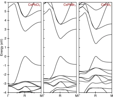
software”. Some example calculations of the band structure of CsPBX3, one of the
recent promising semiconductors for photovoltaics and light-emitting applications, are shown in Fig. 2.1.1.
There are a number of basic features of the band structures of semiconductors, as seen from Fig. 2.1.1. The lowest unoccupied band right above the VBM, called
the conduction band (CB), is separated from the VBM by an energy gap Egap. The
Figure 2.1.1: Example calculations using VASP of the band structures of CsPbX3, where
X=Cl, Br or I. The figure is taken from Supp. Info. of Ref. [99]. All N0valence electrons
fill the electronic levels up to the valence band maximum that is set to be at 0 eV.
an electron from a valence band to a conduction band, one needs to provide an
amount of energy of at least Egap. One common problem with DFT is the
underes-timation of Egap, as for the case of perovskites. In addition to this, around a high
symmetry point, for instance the R-point at the band gap of CsPBX3, the
cur-vatures of the electronic bands also incorrectly underestimate the reduced masses in the bulk [99] as compared to the measured values [132, 53, 84]. One way of attempting to deal with these problems is to employ the GW method. Using the wave functions and energy levels from the DFT calculations, the GW approxima-tion takes into account the electronic correlaapproxima-tion more properly by using the
many-body Green function method. Roughly speaking, a correlation functional ΣN0 will
be used, in place of UN0
HF or any other mean-field potential UmfN0, for treating the
Coulomb interaction. All the software listed above can be extended, in principle, to include GW approximation though at the price of much heavier computations. Example calculations of GW method can be found in [122, 1].
The calculations of the band structure based on DFT or GW methods are referred to as ab initio calculations in this thesis. They provide the useful inputs,
such as the band gap Egap and the effective masses of the band edge, for the k · p
2.2 k · p model
When an electron is promoted from the valence band to the conduction band, an ‘exciton’ is created where the electron stays in the conduction band and the ‘hole’, a missing electron, in the valence band. The curvatures of the conduction and
valence bands around the band gap are interpreted as the ‘effective masses’ m∗
eand
m∗
hof the electron and hole respectively. Note that VBM has a negative curvature,
which implies that m∗
his positive.
Figure 2.2.1: Calculated band structure of In0.5Ga0.5As, taken from Ref. [109], using
three different methods: the 8 × 8 k · p method (dotted lines), the tight-binding like effective bond-orbital method (solid lines) and the empirical sp3s∗tight-binding method
(dashed lines). The 8 × 8 k · p method works very well around the Γ point where the direct band gap occurs, as typical for GaAs, CdSe etc.
Fig. 2.2.1 shows an example band structure of In0.5Ga0.5As calculated using
three different methods. The k · p theory agrees very well with the other two numerical methods in reproducing the band edge structure around the Γ point (i.e. wave vector �k = 0), where there is the direct band gap. Moving away from �k = 0 at the Γ point, some deviations start to appear, which possibly are caused by insufficient number of included bands (since only 8×8 k·p model was used) and other atomistic effects. In an excitonic system, the electron(s) and hole(s) relax to CBm and VBM respectively, after the initial excitation, via phonon emission on the time scale of picoseconds. Therefore, only the valence and conduction band edges at �k = 0 are important and the k ·p theory renders a simple and adequate description for the electronic energy levels and relevant processes of the electron-hole system. Within the scope of the current thesis, we focus on describing the optical prop-erties of colloidal nanocrystals. Due to the confinement from the shape of nano-structure, the full wave function of a particle no longer belongs purely to the bulk conduction or valence band. In other words, the confining potential mixes the vari-ous bands at the band edge as well as discretizes the electronic energy levels, which
makes a nanocrystal look like an ‘artificial’ atom. The full wave function ψa(�r)of
a particle state |ψa� in 2n × 2n k · p model is
ψa(�r) =
n
�
α=1
ψaα(�r), where ψaα(�r) = ξaα(�r) uaα,0(�r). (2.2.1)
The wave function ψaα(�r)can be expressed as in (2.2.1) thanks to the separation
of length scale, for which the Bloch part uaα,0(�r) is periodic w.r.t. the unit cells
(microscopic, atomic length scale) while ξaα(�r) varies over the whole mesoscopic
nanocrystal. The information about symmetry and degeneracy of the bands at
�k = 0 is contained inside the Bloch functions uaα,0(�r). The envelope parts ξaα(�r)
of the full wave function ψa(�r)describe the particle at mesoscopic length scale.
The remaining part of this chapter is devoted to deriving the radial form for
the k · p Hamiltonian and the envelope functions ξaα(�r). This will provide a theory
for the mesoscopic length scale, which is much more computationally efficient than the atomistic approaches. We shall make the basic assumption that the same bulk parameters can be used for the confined nanocrystal systems. For the very small nanocrystals, especially those having less than 10 atomic layers in each dimension, the assumption about using the bulk parameters may not strictly hold true. This range of sizes may introduce certain atomistic effects, for example the distortions from the bulk lattice crystals, surface defects, etc. Hence, an ab initio approach might be desirable here. Nonetheless, for a sizable nanocrystal with more than several thousands of atoms, the band structure parameters get closer to the bulk values throughout the whole nanocrystal while the atomistic-level calculations be-come too expensive or even infeasible. In this case, the k · p model in combination with the envelope function approximation is extremely advantageous.
In Chapters 2 and 3, we treat both the 8 × 8 k · p model (for group III-V and II-VI semiconductors) and the 4×4 k·p model (PbS, PbSe and perovskites). After
obtaining the radial k·p Hamiltonian Hk·pin this chapter, we shall derive the radial
Hartree-Fock potential, which is a mean-field approximation, in Chapter 3. Then, the Hartree-Fock equations can be utilized to generate a single-particle (mean-field) basis for the many-body perturbation theory in Chapters 4 and 5. In those two chapters, the calculations of the correlation energy and the optical response focus on the 4 × 4 k · p model having perovskites as the materials for applications.
2.2.1 Eight-band k · p model
As a reminder, the band structure at �k = 0 (the band gap) of the common semi-conductors such as GaAs, InAs, CdSe, CdS etc. can be well described using the
8× 8 k · p model. The lowest conduction band has an approximate s-wave
symme-try, thus called an s-like band, with two-fold degeneracy from spin [41]. Meanwhile, the valence band is p-like and is split further into two subbands due to spin-orbit coupling of the constituent heavy metal (Ga, Cd, . . . ), see [40, 78] for more details. Let �L be the orbital angular momentum and �S be the electron spin associated with the Bloch functions. The spin-orbit coupling implies that only the Bloch
total angular momentum �J = �L + �S, also called the pseudospin �J, is the conserved
p3/2and p1/2 corresponding to J = 3/2 and J = 1/2. At �k = 0, their degeneracy
(2J + 1)equals 4 and 2 respectively. As the wave vector �k becomes non-zero, the
p3/2band splits into a light hole branch with more negative curvature and a heavy
hole branch that lies above the light hole. Figure 2.2.2 is a schematic of an 8×8 k·p model of the band structure at around the band edge.
SOC
Figure 2.2.2: The schematic of the 8 × 8 k · p. The s1/2conduction band and the (spin
split-off) p1/2 valence band are two-fold degenerate. At �k = 0, the p3/2 valence band
is four-fold degenerate. Away from |�k| = 0, the p3/2 band constitutes of two branches
with different curvatures. These are called the light and heavy holes. The p3/2and p1/2
bands are further coupled to s1/2 via (−�p · �∇), where (−�∇) is the momentum opertor
�k in position space representation. We have chosen the convention where a momentum operator is real and the complex unit i has been omitted.
The effective Hamiltonian for the kinetic energy of a hole can be described by the 8 × 8 k · p model as [39]
Hkin= Hk·p8×8=−(Ac∇2+ Egap)Ic− �p · �∇ + Hk·p6×6Iv+ Hsoc. (2.2.2)
In the above, Hsocrepresents the spin-orbit coupling in the p-like valence band.
Its effect is to put the p1/2band below the p3/2 band by an energy difference Δsoc.
The operator Ic/vacts on a conduction/valence state as the identity and equals to
0 otherwise. The block −(Ac∇2+ Egap) Ic captures a portion of the conduction
band kinetic energy. The 6 × 6 block H6×6
k·p describes the properties of the valence
band including the p3/2and p1/2subbands. One has that
H6×6 k·p = 1 2γ1∇ 2+ γ(� ∇ · �L)2, (2.2.3)
where �L acts on the Bloch function part of the total wave function. The idea be-hind Eq. 2.2.3 is a Hamiltonian that has quadratic dependence on the momentum operator, in other words quadratic in �∇, meanwhile possesses rotational
invari-ance. We note that the coefficients γ1and γ in (2.2.3) are precisely the Luttinger
The term (−�p · �∇) is the k · p coupling between the s1/2band and the p3/2and
p1/2bands. It will become clear later in this chapter that (−�p · �∇) is proportional
to �Ep, where Epis the Kane parameter. The operator �∇ acts on the envelope
parts ξaα(�r)of the total wave function while �p = �∇(L)acts only on the orbital parts
of the Bloch functions uaα,0(�r).
In the bulk, both the pseudospin �J and the wave vector �k are conserved
quan-tities. In a confined system, �Jand �k of the total wave function are no longer good
quantum numbers. Instead of �k, the envelope degree of freedom can be more conve-niently classified by its orbital angular momentum �l. The total angular momentum
�
F = �J +�l, of a single-particle state, is a good quantum number of the Hamiltonian
H8×8
k·p. In other words, the operator �F commutes with Hk·p8×8, for which we shall now
give a proof. For a system with an overall spherical symmetry, the total angular
momentum should be a good quantum number in principle. It is obvious that �F
commutes with −(Ac∇2+ Egap)Ic. The operator �l commutes with ∇2because the
eigen functions |lml� of the former are also eigen functions of the Laplacian ∇2. On
the other hand, ∇2contains no dependence on �J and, as a result, must commute
with �J.
Therefore, it remains to show that (−�p · �∇) and H6×6
k·p also commute with �F.
Next, we shall show that��p· �∇, �F�= 0.
Let �ijk be the Levi-Civita symbol. Note the following commutation identities
[pi, Lj] = i� � k �ijk pk, [∇i, lj] = i� � k �ijk∇k. (2.2.4)
By applying the identities in (2.2.4) to the commutator��p· �∇, Fj
� , where � �p· �∇, Fj � =� i (pi[∇i, Lj] + [pi, lj]∇i) , (2.2.5)
and recalling that �ijkis anti-symmetric upon exchanging any two indices, one has
� �p· �∇, Fj � =� ik i� (�ijk∇ipk+ �ijk∇kpi) = 0. (2.2.6)
Now, we prove that the commutator�Hk·p6×6, �F�is also zero.
In Eq. (2.2.3), the first term 1
2γ1∇2commutes with �F. Therefore, to show that
H6×6
k·p commutes with �F, one only needs that
� (�∇ · �L)2, �F�= 0. � (�∇ · �L)2 , Fj � =�(�∇ · �L)2 , lj � +�(�∇ · �L)2 , Jj � , (2.2.7)
where �∇ · �L =�k∇kLk and � (�∇ · �L)2, J j � =�(�∇ · �L)2, L j � . Therefore, � (�∇ · �L)2, F j � = i�� i1i2 � � k2 �i2jk2∇i1∇k2+ � k1 �i1jk1∇k1∇i2 � Li1Li2 + i�� i1i2 ∇i1∇i2 � � k2 �i2jk2Li1Lk2+ � k1 �i1jk1Lk1Li2 � . (2.2.8)
With a change of notation for the sum, � i1i2k2 �i2jk2∇i1∇k2Li1Li2= � i1k2i2 �k2ji2∇i1∇i2Li1Lk2=− � i1i2k2 �i2jk2∇i1∇i2Li1Lk2, � i1i2k1 �i1jk1∇k1∇i2Li1Li2= � k1i2i1 �k1ji1∇i1∇i2Lk1Li2=− � i1i2k1 �i1jk1∇i1∇i2Lk1Li2. (2.2.9) Substituting (2.2.9) to (2.2.8), we get �(�∇ · �L)2, F j �
= 0, which completes the
proof of �F being a good quantum number for H8×8
k·p . Thus, an eigenstates of Hk·p8×8
can be classified by the total angular momentum �F and takes the form |F M�.
It is also clear from the above derivation that (�∇ · �L)2does not commute with
either �l or �J. Thus, (�∇ · �L)2 generally mixes the Bloch states with J = 1/2 and
J = 3/2.
Consider the ∇1
q component of �∇ = ∇1, which is a rank-one spherical tensor.
∇1
q maps |lml� to |l ± 1 ml+ q�. As a consequence, (−�p · �∇) connects |lml� to
|l�m
l��, where l�= l± 1, and (�∇ · �L)2connects |lml� to |l�ml��, where l�= l, l± 2.
It means that within the valence band, the various states | (l, J) F M� for the same
(F, M )with different l and J are coupled to each other. These coupled states can
have both J = 1/2 and J = 3/2.
Let l be the smallest envelope angular momentum among these coupled states. From the triangle inequality (l, J, F ), there is a number of cases, depending on the relation between l and F :
• If l = F −3
2 for F ≥
3
2, there are four coupled states
|�l, p3 2 � F M�, |�l + 2, p3 2 � F M�, |�l + 2, p1 2 � F M� and |�l + 1, s1 2 � F M�. • If l = F −1 2 for F ≥ 3
2, the four coupled states are
|�l, p3 2 � F M�, |�l + 2, p3 2 � F M�, |�l, p1 2 � F M� and |�l + 1, s1 2 � F M�. • If F =1
2, there are two sets of three coupled states
|�l = 1, p3 2 � F =1 2M�, | � l = 1, p1 2 � F =1 2M� and | � l = 0, s1 2 � F =1 2M�, |�l = 0, p3 2 � F =1 2M�, | � l = 0, p1 2 � F =1 2M� and | � l = 1, s1 2 � F =1 2M�.
We would like to remind the readers again that each of the coupled states |(l, J)F M� contains information about the corresponding Bloch function and its
transformation properties. In what follows, the Bloch functions uaα,0(�r)in the full
wave function |ψa� (see Eq. (2.2.1)) will be implicit in the k · p components of the
We conclude that for F ≥ 3
2, the total wave function |a� of an eigenstate can
be written explicitly as a sum of four components
|a� = 1 r � Ra1(r)|(l + 1, s12)F M� + Ra2(r)|(l, p32)F M� +Ra3(r)|(l + 2, p32)F M� + Ra4(r)|(l + 2, p12)F M� � , if l = F −3 2, 1 r � Ra1(r)|(l + 1, s12)F M� + Ra2(r)|(l, p32)F M� +Ra3(r)|(l + 2, p32)F M� + Ra4(r)|(l, p12)F M� � , if l = F −1 2. (2.2.10)
For the special case F = 1
2, there are only three coupled components, as establish
above, and one has
|a� = 1 r � Ra1(r)|(l − 1, s12)F M� +Ra3(r)|(l, p32)F M� +Ra4(r)|(l, p12)F M� � , if l = F +1 2, 1 r � Ra1(r)|(l + 1, s12)F M� + Ra2(r)|(l, p32)F M� +Ra4(r)|(l, p12)F M��, if l = F −12. (2.2.11)
Any missing k · p component, which is understood to be zero, in Eq. (2.2.11) is due to the corresponding orbital angular momentum �l being negative or not satisfying the triangle inequality (l, J, F ). By using the convention that α, where
α = 1, . . . , 4, indexes the spin-angular basis vector |(lJ)F M�, one can write down
a vector containing only the radial components Ra,α.
The radial form of the total wave function |a� can be written as
|a� = 1r Ra1(r) Ra2(r) Ra3(r) Ra4(r) , (2.2.12)
where the associated angular momentum states are as given in Eqs. (2.2.10) and (2.2.11). For the case of F = 1/2, the missing component with either α = 2 or α = 3, see (2.2.11), is set to zero automatically.
In a confined system, the external potential Vextmixes the various k · p
compo-nents with angular states |(l, J)F M�. The total wave function |a� is an eigenstate of the following equation
�
Hk·p8×8+ Vext�|a� = Ea0|a�. (2.2.13)
When the external potential Vext is spherically symmetric, |a� takes the form
(2.2.10) or (2.2.11). Next, we aim to work out the radial form of H8×8
k·p matrix
of which the radial wave function (2.2.12) is an eigenvector. Roughly speaking,
one can do this by taking the projection �(l, J)F M|H8×8
k·p|a�, where the total wave
function |a� contains the |(l�, J�)F M� k · p components. To achieve this goal, we
The H6×6
k·p defined in Eq. (2.2.3) can be re-written as a sum of spherical tensors,
Hk·p6×6= A0∇2+ A2
� �
∇�∇�2· T2
. (2.2.14)
The rank-zero tensor operator ∇2 commutes with �l and does not act on the
Bloch part. Therefore, ∇2 does not mix any of the components in Eq. (2.2.12).
From the matrix element �l l|∇2
|l l�, see Eq. (B.2.10), the action of ∇2 on each
radial component takes the simple expression
�(l, J)F M|∇2 |(l, J)F M� =r12 ∂ ∂r(r 2 ∂ ∂r)− l(l + 1) 1 r2. (2.2.15)
About the second term, both�∇�∇� �2 and T2 are rank-two spherical tensors.
While�∇�∇� �2 acts on the envelope degree of freedom, T2 operates on the Bloch
part of the total wave function. From the results of Section B.2 in the appendix, one
easily sees that�∇�∇� �2·T2generally mixes the various k·p components |(l, J)F M�
of the total wave function. By applying the results (B.4.4) of the appendix Section
B.4, the action of�∇�∇� �2· T2is �(l, J) F M|�∇�∇� �2· T2 | (l�, J�) F M� =(−1)l+J+F l l� 2 J� J F × �J||T2 ||J�� �l||�∇�∇� �2||l��, (2.2.16) where l�= lor l ± 2.
A complete derivation of the reduced matrix element �l||�∇�∇� �2||l�� are given
in appendix Section B.2. It remains to evaluate �J||T2||J��. We must note that,
being a rank-two tensor, T2 connects only the p-like states, which have L = 1. We
define T2 such that, for L = 1,
�L||T2
||L� = 1. (2.2.17)
From the definition (2.2.17), one can deduce the reduced matrix element �J||T2||J��
by applying the formulas (B.3.2) and (B.3.3) to get
�J||T2 ||J�� = (−1)L+1/2+J� × [J]1/2[J�]1/2 × 2 J J� 1/2 1 1 . (2.2.18)
With this choice of T2, the coefficient A
0 and A2 in (2.2.14) are related to the
Luttinger parameters γ1and γ, see the expression (2.2.3) for Hk·p6×6, as follows
�
A0=12γ1,
A2=−3
√
The relations in (2.2.19) can be derived by relating the parameters A0 and A2 to
the effective masses m∗
lhand m∗hhof the light and heavy holes in the bulk limit at
�k = 0. One can obtain a similar relation between {m∗
lh, m∗hh} and {γ1, γ}.
The last remaining term of H8×8
k·p to be expressed in radial form is (−�p · �∇). We
need, in particular, the matrix element �(l,1
2)F M|�p· �∇|(l�, J)F M�, where l�= l±1.
Applying the results of the appendix B.4 leads to
�(l,1 2)F M|�p · �∇| (l �, J) F M� =(−1)l+3/2+F l l� 1 J 1/2 F × �(s,12)1 2||�p||(p, 1 2)J� �l||�∇||l ��, �(l�, J) F M|�p · �∇|(l,1 2)F M� =(−1) l+J+F l� l 1 1/2 J F × �(p,1 2)J||�p||(s, 1 2) 1 2� �l �||�∇||l�. (2.2.20)
The reduced matrix element �l||�∇||l�� (or �l�||�∇||l�) can be found in Eq. (B.1.6),
see the appendix Section B.1. Regarding �(s,1
2) 1
2||�p||(p,
1
2)J�, the spherical tensor
�pacts on the first angular momenta �L, where s and p stand for L = 0 and L = 1
respectively. Due to the parity selection rule, �p connects only between L = 0 and
L = 1but not among the L = 1 states themselves. By using the final result of
Section B.3, the explicit expressions for the reduced matrix elements of �p are given as �(s,12)1 2||�p||(p, 1 2)J� = (−1) 3 2+J�2[J] 1 1/2 J 1/2 1 0 �0||�p||1�, �(p,12)J||�p||(s,1 2) 1 2� = − � 2[J] 1 J 1/2 1/2 0 1 �1||�p||0� =−�2[J] 1 1/2 J 1/2 1 0 �0||�p||1�. (2.2.21)
Now, we introduce the following shorthand notations for three radial operators that will appear frequently later on.
Ll= d2 dr2− l(l + 1) 1 r2, (2.2.22) Ml= d2 dr2+ (2l + 3) 1 r d dr+ l(l + 2) 1 r2, (2.2.23) Dl= d dr − (l + 1) 1 r. (2.2.24)
With the above definitions for Ll, Mland Dl, one can write down the radial Hk·p8×8
Again, the radial H8×8
k·p takes two explicit forms depending on the exact relation
between l and F . In Eqs. (2.2.25) and (2.2.26), we provide the radial expressions
for H8×8
k·p when all four radial components are present, i.e. when F ≥ 32. When
(F = 1
2, l = 1)and (F =
1
2, l = 0), the rows and columns containing the index
α = 2or α = 3, see Eq. (2.2.11), are set to zero.
If l = F −3
2, the radial form of H
8×8 k·p can be found to be Hk·p8×8= −AcLl+1+ Egap −c 3 2 l+1,lDl −c 3 2 l+1,l+2Dl+1† −c 1 2 l+1,l+2Dl+1† −c32∗ l+1,lD†l (A0− A2δ 3 232 l )Ll A2σ 3 232 l,l+2Ml A2σ 3 212 l,l+2Ml −c32∗ l+1,l+2Dl+1 A2σ 3 2 3 2 l,l+2M†l (A0− A2δ 3 2 3 2 l+2)Ll+2 −A2δ 3 2 1 2 l+2Ll+2 −c12∗ l+1,l+2Dl+1 A2σ 1 232 l+2,lM†l −A2δ 1 232 l+2Ll+2 A0Ll+2− Δsoc . (2.2.25) Or else, if l = F −1 2, one has Hk·p8×8= −AcLl+1+ Egap −c 3 2 l+1,lDl −c 3 2 l+1,l+2Dl+1† −c 1 2 l+1,lDl −c32∗ l+1,lD†l (A0− A2δ 3 232 l )Ll A2σ 3 232 l,l+2Ml −A2δ 3 212 l Ll −c32∗ l+1,l+2Dl+1 A2σ 3 2 3 2 l,l+2M†l (A0− A2δ 3 2 3 2 l+2)Ll+2 A2σ 3 2 1 2 l+2,lM†l −c12∗ l+1,lD†l −A2δ 1 232 l Ll A2σ 1 232 l,l+2Ml A0Ll− Δsoc . (2.2.26)
The radial expressions of H8×8
k·p above are the ones describing a hole, where
the valence band consists of the light hole, heavy hole and p1/2 hole bands. The
Hk·p8×8 for an electron receives just an overall minus sign compared to (2.2.25) and
(2.2.26).
The coefficients δJJ�
l , σJJ
�
l,l� and cJl+1,l�, which result from (2.2.14)-(2.2.24), can
be given as δJJ� l = (−1)l+J+F � 2 3 l(l + 1)(2l + 1) (2l− 1)(2l + 3) l l 2 J� J F �J||T 2 ||J��, (2.2.27) σJJ� l,l� = (−1)l+J+F � (lmin+ 1)(lmin+ 2) 2lmin+ 3 l l� 2 J� J F �J||T 2 ||J��, (2.2.28)


![Figure 2.2.1: Calculated band structure of In 0.5 Ga 0.5 As, taken from Ref. [109], using three different methods: the 8 × 8 k · p method (dotted lines), the tight-binding like effective bond-orbital method (solid lines) and the empirical sp 3 s ∗ tight-bind](https://thumb-eu.123doks.com/thumbv2/123doknet/12692432.355055/25.739.168.533.255.511/figure-calculated-structure-different-methods-binding-effective-empirical.webp)