HAL Id: hal-03111203
https://hal.archives-ouvertes.fr/hal-03111203
Submitted on 15 Jan 2021
HAL is a multi-disciplinary open access
archive for the deposit and dissemination of
sci-entific research documents, whether they are
pub-lished or not. The documents may come from
teaching and research institutions in France or
abroad, or from public or private research centers.
L’archive ouverte pluridisciplinaire HAL, est
destinée au dépôt et à la diffusion de documents
scientifiques de niveau recherche, publiés ou non,
émanant des établissements d’enseignement et de
recherche français ou étrangers, des laboratoires
publics ou privés.
Technology
Apolline Puaud, Anne-Sophie Ozanne, Laurie-Lou Senaud, Delfina Munoz,
Charles Roux
To cite this version:
Apolline Puaud, Anne-Sophie Ozanne, Laurie-Lou Senaud, Delfina Munoz, Charles Roux.
Micro-crystalline Silicon Tunnel Junction for Monolithic Tandem Solar Cells Using Silicon
Heterojunc-tion Technology. IEEE Journal of Photovoltaics, IEEE, 2021, 11 (1), pp.58-64.
�10.1109/JPHO-TOV.2020.3038600�. �hal-03111203�
Microcrystalline Silicon Tunnel Junction for
Monolithic Tandem Solar Cells using Silicon
Heterojunction Technology
Apolline PUAUD
1, Anne-Sophie OZANNE
1,
Laurie-Lou SENAUD
2, Delfina MUNOZ
1and Charles ROUX
11. CEA-INES, 50 Avenue du lac Léman, Le Bourget-du-Lac, F-73375, France
2.
CSEM, PV-Center, Rue Jaquet-Droz, CH-2002 Neuchâtel, Switzerland
Abstract—In this study, we developed a microcrystalline silicon
tunnel junction to be used as a tunnel recombination junction between a large-gap top-cell and a silicon heterojunction bottom-cell, in a monolithic tandem integration. This junction is composed of a p-type layer on the top of an n-type layer, deposited by plasma-enhanced chemical vapor deposition at low temperature (200°C). Microcrystalline phase percentage was controlled with Raman spectroscopy and ellipsometry measurements. The total stack has a thickness of 40 nm and an average conductivity around 10 S/cm. Minority carrier lifetime measurements showed an improvement of the field effect and the passivation with the addition of this junction on top of silicon heterojunction solar cells. Moreover, implementation of microcrystalline layer on top of reference rear emitter silicon heterojunction solar cells improved the fill factor and did not induce parasitic absorption above 700 nm. Simple tests structures were fabricated in order to characterize the tunnel junction and optimize it. Then, we carried out dark temperature-dependent I-V measurements on those test structures and observed peaks and valleys, characteristic of the junction tunnel behavior. The developed tunnel junction shows low contact resistivity and activation energies these are promising results for the complete integration on the tandem device.
Index Terms—Microcrystalline Silicon, Silicon Heterojunction,
Tandem Solar Cells, Tunnel Recombination Junction
I.INTRODUCTION
Silicon based single-junction solar cells record efficiencies [1] are getting closer to their practical limit highlighted by K. Yoshikawa et al. [2]. In this context, tandem and multi-junction solar cells are a great solution to reach more than 30% efficiency. With their high power conversion efficiencies over 25%, silicon heterojunction solar cells (SHJ) are very promising candidates as bottom-cell for monolithic tandem solar cells [1]. In fact, the key of the SHJ technology is the very high open-circuit voltage (Voc) achieved by amorphous silicon passivation, over 740mV [3]. Their fabrication process has demonstrated to be cost effective (e.g. Panasonic, Hevel, Enel Green Power, REC…) and their architecture permits a rear or a front emitter and high bifaciality ratio [4]. Moreover, as a bottom-cell in monolithic tandems, SHJ cells only absorb in the infrared range, so the parasitic absorption in the near UV range of amorphous silicon layers (a-Si:H) do not generate short-circuit current losses. Such tandem solar cells with SHJ bottom-cell demonstrated efficiency of 20% with GaAsP
top-cell [5] and efficiencies up to 29.15% with perovskite based top-cell [6].
To obtain a good monolithic tandem, the junction between the two sub-cells is a key feature. This junction, usually named tunnel recombination junction (TRJ) should be thin, transparent and conductive to allow the charge carriers to recombine. In multijunction solar cells, tunnel junctions interconnect the sub-cells and prevent the formation of parasitic p-n junctions [7]. In the case of monolithic perovskite/silicon tandem solar cells, Mailoa et al. [8] first demonstrated the feasibility of this kind of silicon tunnel junction, in 2015, using hydrogenated amorphous silicon partially crystallized by an annealing at 680°C. Then, in 2019, two groups proposed a (n+)poly-Si/(p+)poly-Si tunnel junction for high-temperature passivated contact bottom-cells [9], [10]. In parallel, for the same type of bottom-cells, Nogay et al. made a tunnel junction using a silicon carbide layer [11]. With a SHJ bottom cell, tunnel junction layers should not degrade a-Si:H layers’ interfaces, which are sensitive to high temperature. In this context, nano- or microcrystalline silicon that could be processed at low-temperature seems to be a good choice. It also presents some advantages comparing to others recombination junctions, as transparent conductive oxides (TCOs), often used in tandem with a perovskite-based top-cell. In fact, nano- or microcrystalline silicon layers are more transparent in the infrared range and have optical indexes more adapted [12]. Moreover, this type of junction already performed well in several multijunction solar cells [13]–[16] and have all the required qualities. For example, Sahli et al. demonstrated a perovskite/silicon tandem solar cell with a nanocrystalline silicon tunnel junction at low temperature (<200°C) in both standard and rear emitter configurations [13], [17]. The same kind of junction was also used by Tomasi et al. in back-contacted silicon SHJ and performed well [18]. In this work, we choose to develop a tunnel junction in microcrystalline silicon deposited by plasma-enhanced chemical vapor deposition (PECVD) at low temperature (200°C) to preserve the SHJ bottom-cell. Furthermore, the PECVD process of microcrystalline silicon takes place in the same tool than amorphous silicon layers of SHJ cells so the bottom-cell and the TRJ can be produced on the same line. This study focuses on the characterization and the validation of this tunnel junction,, without building an entire tandem. Contrary to the previous presented work, the idea here is not
bottom-cell with a front-side TRJ, adapted for a tandem integration with a large-gap top-cell. In the same way that J. Yang et al. did for standard silicon-based solar cells [19] and Luderer et al. did for a TOPCon bottom-cell [10]. Therefore, we investigated the tunnel junction in three parties: the characterization of the microcrystalline silicon layers, its implementation on the top of an SHJ solar cell and the validation of a sufficient tunneling behavior and a low resistance junction.
II. MATERIALS AND METHODS
Microcrystalline silicon layers were deposited by plasma-enhanced chemical vapor deposition (PECVD) at 200°C. The deposition power was 1100 Watt and the pressure was 9 Torr. To obtain a 20 nm thickness, deposition times were 110 and 80 seconds, for (n+)µc-Si:H and (p+)µc-Si:H layers, respectively. Moreover, we used a H2/SiH4 ratio at 400 and dopants/SiH4 ratios at 1 and 1.2 for (n+)µc-Si:H and (p+)µc-Si:H, respectively.
Symmetrical test samples and SHJ cells are fabricated with industrial processes on n-type Cz commercial wafers, 180 µm, with a resistivity between 0.5 Ω.cm and 1.5 Ω.cm, M2 size. Wafers are received as-cut and are then cleaned and textured with classical chemical treatments (KOH solution and O3 based clean), for detailed information see [20], [21].
Amorphous silicon layers and ITO are deposited respectively by PECVD and PVD in Meyer Burger tools. The metallization is done by physical vapor deposition (PVD) for test samples and screen-printing 5 busbars bifacial design for SHJ cells. Sheet resistance (Rsheet)was measured by 4-wire sensing on 20 nm layers deposited on glass. Spectroscopic ellipsometry measurements were performed with a Horiba Jobin Yvon UVISEL ellipsometer under an incident angle of 70º. Raman spectroscopy was carried out using a 325 nm laser for the layer’s surface (δp ≈ 8 nm) and a 442 nm laser to look more deeply (δp ≈ 50 nm). Minority carrier lifetime and implied parameters were measured by photoconductance decay on a WCT-120 Sinton instrument using the transient mode, shown results are the average of ten measurements for each sample. Light I-V measurements of total cell area were performed
Dark I-V were done with probes on circular electrodes under vacuum. External quantum efficiencies were measured with a 150W Xe lamp spectrally filtered.
III. RESULTS AND DISCUSSION
Material characterization
In order to characterize the developed µc-Si:H layers, we performed electrical and optical measurements. We extracted conductivities from sheet resistances (Table I) and they are more than four orders of magnitude higher than doped amorphous silicon used in SHJ cells. To validate the crystallinity of the layers and determine their thickness, we did spectroscopic ellipsometry measurements on glass and on silicon substrates. Measured pseudodielectric functions (𝜺 = 𝜺𝒓+ 𝒊(𝜺𝒊)) and their fitting curves are shown in Fig.1. We
used a model assuming a mixture of µc-Si:H, a-Si:H and void and extracted layers’ thicknesses (Table I) and percentage of microcrystalline phase (Fig.2). Microcrystalline phase should be controlled not to impact the tandem’s Voc [22], [23]. The hump around 4 eV in 𝜺𝒊 curve is characteristic of the silicon
microcrystallites [24] and confirmed the microcrystalline phase of the developed layers. Moreover, we performed Raman spectroscopy measurements to confirm the percentage of microcrystalline phase obtained by ellipsometry. Raman spectrums were decorrelated in three peaks: 480 cm-1 for the amorphous phase, 520 cm-1 for crystalline silicon and 507 cm -1 for the mix-phase. The microcrystalline phase fraction,
F ig.2 Percentage of microcrystalline phase extracted by spectroscopic ellipsometry and Raman spectroscopy.
TABLEI
RSHEET, CONDUCTIVITY AND THICKNESS OF MICROCRYSTALLINE SILICON LAYERS
Average Rsheet (kΩ) Average Conductivity (S/cm) Best measured Conductivity (S/cm) Average Thickness (nm) (n+) µc-Si:H 25 20 33 21 (p+) µc-Si:H 250 1 2 19 (n+) µc-Si:H/ (p+) µc-Si:H 22 10 13 40
Rsheet and conductivity measured by 4-wire sensing.Thickness extracted by
spectroscopic ellipsometry. 0 20 40 60 80 100 (n+)µc-Si:H on glass (p+)µc-Si:H on glass (n+/p+)µc-Si:H on glass (n+)µc-Si:H on a-Si:H (p+)µc-Si:H on a-Si:H (n+/p+)µc-Si:H on a-Si:H
Average microcrystalline phase fraction, 𝑿(µ𝒄−𝑺𝒊) (%)
Ellipsometry Raman 325 nm Raman 442 nm
𝑿µ𝒄−𝑺𝒊, was calculated using the following equation (adapted
from [25]) :
𝑿µ𝒄−𝑺𝒊=
𝑰𝟓𝟐𝟎+ 𝑰𝟓𝟎𝟕
𝑰𝟓𝟐𝟎+ 𝑰𝟓𝟎𝟕+ 𝝈𝑰𝟒𝟖𝟎
where σ is the ratio of the integrated Raman cross-section for amorphous to microcrystalline silicon (σ≈1, [25]). 𝑰𝟓𝟐𝟎, 𝑰𝟓𝟎𝟕 and 𝑰𝟒𝟖𝟎 are the integrated intensities of the
previous cited Raman peaks. Fig.2 demonstrate that the percentages of microcrystalline phase extracted by Raman spectroscopy and ellipsometry are consistent. In fact, the small differences observed between the two techniques are mainly explained by the fact that ellipsometry affected the entire layer, no matter its thickness, contrary to Raman spectroscopy. Due to the wavelength of the lasers used for Raman spectroscopy, the results obtained with the 325 nm laser (penetration depth: δp ≈ 8 nm) are more related to the surface of the layers. This also explain why the microcrystalline phase percentage measured by Raman spectroscopy is almost the same for the p-type layer and the n+/p+ stack, because only the front p+ layer is measured. However, for the samples measured with the 442
nm laser (δp ≈ 50 nm), obtained results represent the entire stack. This explains why the microcrystalline phase fraction is a bit lower than with ellipsometry for samples on a-Si:H (structures presented Fig.1 (c) and (d)), because the amorphous layers (between 10 and 15 nm) are included. In fact, in the model used to fit ellipsometric data, the amorphous layers are included in one pure amorphous layer and not in the mixed layer referring to microcrystalline silicon. Table I shows that we achieved a forty nanometers PN junction. Microcrystalline silicon layers have very good conductivities, around 10 S/cm and a controlled microcrystalline phase percentage.
Microcrystalline silicon on the top of SHJ solar cells
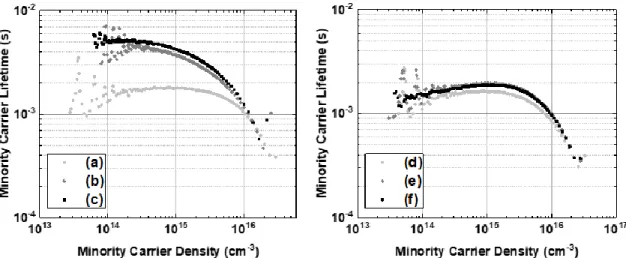
Minority carrier lifetime measurements were performed after the PECVD process. Fig. 3 and Table II illustrate the improvement of passivation for symmetric structure (a) (Fig.4) with the addition of the microcrystalline silicon layers (structures (b) and (c)). In fact, the lifetime is more than doubled with the tunnel junction. This improvement is induced by the high level of hydrogen during the deposition, which will Fig. 1 Plot of the pseudodielectric function (dotted lines) measured by spectroscopic ellipsometry and corresponding fitting curves (lines). A) microcrystalline
silicon n-type layer on glass; B) microcrystalline n-p junction on glass ; C) n-type microcrystalline layer on silicon substrate/(i) a-Si:H/(n) a-Si:H ; D) n-p microcrystalline junction on silicon substrate/(i) a-Si:H/(n) a-Si:H. The region characteristic of silicon microcrystallites is circled with dotted line for glass
passivate silicon dangling bonds. Moreover, the high conductivity of microcrystalline silicon layers compare to amorphous layers will increase the field effect. For rear emitter heterojunction samples, structure (d), the addition of microcrystalline silicon (structures (e) and (f)) is a bit beneficial and do not degrade the passivation. With the µc-Si:H layers on top of the cells (structure (f)), the gain in iFF cannot be as high as in structure (c) because of the limitation induced by the rear emitter (p-type a-Si:H layer). Furthermore, we observed an implied Voc improvement. As expected by using a PECVD process at low temperature, the deposition of µc-Si:H layers do not degrade SHJ solar cells. Contrariwise, adding the microcrystalline tunnel junction tends to improve them by a better chemical passivation and increased field effect.
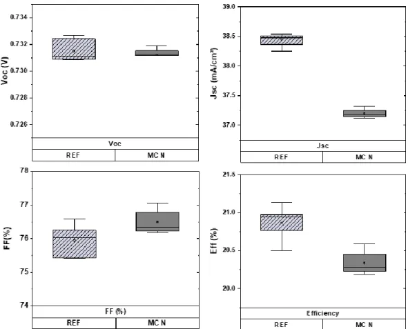
To validate this conclusion, we made two batches of 10 SHJ solar cells, one classical rear-emitter (REF batch) and one with the n-type microcrystalline silicon layer on the top of the
amorphous one (MC N batch), Fig.5. The two batches endured exactly the same fabrication and characterization processes, except the microcrystalline silicon layer deposition for the MC N batch. Post-PECVD minority carrier lifetime measurements presented Table III show better implied parameters (iFF and iVoc) and an increased lifetime for the batch MC N. This validates an improvement of the passivation with the addition of the microcrystalline layer ((n+)µc-Si:H)). Thus, this results in better fill factors, more than 0.5% in average, for the MC N batch (Fig. 6). However, there is a non-negligible but expected
TABLEIII
MINORITY CARRIER LIFETIME AT 1.0E+15Δn AND CORRESPONDING IFF AND IVOC
Average iVoc (mV) Average Lifetime at 1.0E+15 Δn (µs) Average iFF (%) REF 733 2600 84.1 MC N 734 2900 84.2
Measured by the Sinton Instruments tools. TABLEII
MINORITY CARRIER LIFETIME AT 1.0E+15Δn AND CORRESPONDING IFF AND IVOC
Structures iVoc (mV) Lifetime at 1.0E+15 Δn (µs) iFF (%) (a) / 1790 81.2 (b) / 3720 83.9 (c) / 4240 84.4 (d) 732 1630 84.3 (e) 735 1940 84.6 (f) 735 1880 84.5
Measured by the Sinton Instruments tools.
F ig.3 Minority carrier lifetime vs Minority carrier density (Δn) of the studied structures, presented in Fig.4, measured by the Sinton Instruments tools.
Symmetric structures are presented on the left sub-figure and rear emitter heterojunction structures on the right sub-figure.
Fig.5 Schema of the solar cells corresponding to the two batches. REF:
classical SHJ; MC N: SHJ with (n+) µc-Si:H on the top.
loss in current by the addition of the 20 nm (n+)µc-Si:H layer due to parasitic absorption in the visible range. In order to confirm this hypothesis, we made spectral response measurements (Fig. 7) and observed that the loss occurs between 300 and 700 nm. In this single-junction solar cell case, the current loss of 1.2 mA/cm² induces an average loss in efficiency of 0.5%. This will not be a problem in tandem application because the top-cell will fully absorb in the visible range.Furthermore, there is no significant difference between the two solar cells batches in term of Voc. However, series
resistance are lower in structures with the (n+)µc-Si:H layer. This tends to prove that the contact (n+)µc-Si:H/ITO has a lower contact resistivity than the contact (n)a-Si:H/ITO, as Nogay et al. already observed [26]. This study confirmed that adding microcrystalline silicon layers on the top of SHJ cells do not induce undesirable effect for tandem application.
Tunnel junction behaviour
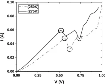
With the goal to validate the operation of the developed microcrystalline silicon tunnel junction, without building an entire monolithic tandem, we performed dark I-V measurements. We made a frontside circular plot of ITO/Ag deposed by masked PVD and a backside full surface ITO/Ag contact on structures (a), (b) and (c) (Fig.4). With this configuration, we observed the (n+)µc-Si:H/(p+)µc-Si:H tunnel junction as a tunnel diode associated in series with a resistance, forming by the others n-type layers. Fig. 8 shows the I-V curves measured at two temperatures, we observe peaks and valleys, characteristic of a tunnel diode. We noted a plateau region in the decrease from the peak current to the valley current minimum, this plateau is known as an indication of oscillation in the negative resistance region of the curve [27]. Moreover, peak currents are much higher than Jsc, which is required for a normal operation of the tunnel junction in multijunction solar cells, according to Yang et al. [19]. As expected, dark I-V curves demonstrate the tunnel effect in the developed (n+)µc-Si:H/(p+)µc-Si:H tunnel junction and validate its high recombination efficiency. In parallel, with the method presented by Luderer et al. [28], we extracted the Fig. 7 External quantum efficiency of the best cells of each batch.
Si:H/(n+)µc-Si:H/(p+)µc-Si:H/ITO/Ag (front-side of the structure (c), Fig.4) from ohmic (R² > 0.994) dark I-V curves, from -100 mV to 100 mV. We obtained values between 0.45 Ω.cm² and 0.55 Ω.cm² at 300K. Temperature-dependent contact resistivity values are in the same range and follow the same trend as the contact resistivity calculated by Nogay et al.
[26] for the (p+)µc-Si:H/ITO/Ag stack. This demonstrates that
the contact resistivity is dominated by the contact with the ITO layer and that the (n+)µc-Si:H/(p+)µc-Si:H junction presents a low contact resistivity. By plotting the contact resistivity in an Arrhenius plot –not shown here- between 250K and 350K we extracted low activations energies, from 75 meV to 150 meV, for both frontside stacks of the structures (b) and (c) (Fig.4). This demonstrates that the tunnel junction behavior is temperature-independent, as expected for a tunnel effect.
IV. CONCLUSIONS
To sum up, we have demonstrated a microcrystalline silicon tunnel junction easily integrated on the top of silicon heterojunction (SHJ) solar cells, for monolithic tandem applications. We controlled the microcrystalline phase percentage in order to maximize its recombination potential and obtained very good conductivities, around 10 S/cm for the entire junction. On top of that, we observed an increase of minority carrier lifetime which shows that the (n+)µc-Si:H/(p+)µc-Si:H layers improve the SHJ solar cells chemical passivation and field effect. Furthermore, those improvements induce a fill factor enhancement. Moreover, the current losses linked to the addition of microcrystalline silicon layers on top of SHJ cell will have no impact in tandem configuration. Finally, with a simple test structure and dark I-V measurements, we completed the tunnel junction characterization and validated its behavior as a low-resistive tunnel recombination junction.
Some supplementary studies are in progress to investigate more deeply the dark I-V measurements and reproduce this method to compare several n+/p+ TRJ for tandem solar cells.
Si:H/(p+)µc-Si:H tunnel junction and a perovskite based top-cell will be presented in future works.
ACKNOWLEDGMENTS
The authors would like to thank C. Ballif and The Photovoltaics-Laboratory (PV-Lab) of IMT for the access to the Raman equipment. This work was funded by the Agence Nationale de la Recherche (ANR) as part of the Carnot program in the Si Premium project.
REFERENCES
[1] M. A. Green, E. D. Dunlop, J. Hohl‐Ebinger, M. Yoshita, N. Kopidakis, and X. Hao, ‘Solar cell efficiency tables (version 56)’,
Prog. Photovolt. Res. Appl., vol. 28, no. 7, pp. 629–638, Jul. 2020, doi:
10.1002/pip.3303.
[2] K. Yoshikawa et al., ‘Silicon heterojunction solar cell with interdigitated back contacts for a photoconversion efficiency over 26%’, Nat. Energy, vol. 2, no. 5, p. 17032, May 2017, doi: 10.1038/nenergy.2017.32.
[3] D. Adachi, J. L. Hernández, and K. Yamamoto, ‘Impact of carrier recombination on fill factor for large area heterojunction crystalline silicon solar cell with 25.1% efficiency’, Appl. Phys. Lett., vol. 107, no. 23, p. 233506, Dec. 2015, doi: 10.1063/1.4937224.
[4] A. Danel, ‘Bifaciality Optimization of Silicon Heterojunction Solar Cells’, presented at the EU PVSEC 2019, Marseille, FRANCE, Sep. 2019, [Online]. Available:
https://www.eupvsec-planner.com/presentations/c48234/bifaciality_optimization_of_silicon_ heterojunction_solar_cells.htm.
[5] S. Fan et al., ‘20%-efficient epitaxial GaAsP/Si tandem solar cells’,
Sol. Energy Mater. Sol. Cells, vol. 202, p. 110144, Nov. 2019, doi:
10.1016/j.solmat.2019.110144.
[6] Helmholtz Zentrum Berlin HZB, ‘World Record: Efficiency of perovskite silicon tandem solar cell jumps to 29.15 per cent’, Jan. 29, 2020.
https://www.helmholtz-berlin.de/pubbin/news_seite?nid=21020;sprache=en;seitenid=1. [7] M. Fillali and B. Dennai, ‘Impact of tunnel heterojunction
(InGaP/GaA) doping concentration on the performance of InGaP/GaAs tandem solar cells using Silvaco-Atlas software’, p. 8.
[8] J. P. Mailoa et al., ‘A 2-terminal perovskite/silicon multijunction solar cell enabled by a silicon tunnel junction’, Appl. Phys. Lett., vol. 106, no. 12, p. 121105, Mar. 2015, doi: 10.1063/1.4914179.
[9] R. Peibst et al., ‘From PERC to Tandem: POLO- and p + /n + Poly-Si
Tunneling Junction as Interface Between Bottom and Top Cell’, IEEE
J. Photovolt., vol. 9, no. 1, pp. 49–54, Jan. 2019, doi:
10.1109/JPHOTOV.2018.2876999.
[10] C. Luderer, C. Reichel, F. Feldmann, M. Bivour, and M. Hermle, ‘Passivating and low-resistive poly-Si tunneling junction enabling high-efficiency monolithic perovskite/silicon tandem solar cells’, Appl.
Phys. Lett., vol. 115, no. 18, p. 182105, Oct. 2019, doi:
10.1063/1.5120552.
[11] G. Nogay et al., ‘25.1%-Efficient Monolithic Perovskite/Silicon Tandem Solar Cell Based on a p -type Monocrystalline Textured Silicon Wafer and High-Temperature Passivating Contacts’, ACS
Energy Lett., vol. 4, no. 4, pp. 844–845, Apr. 2019, doi:
10.1021/acsenergylett.9b00377.
[12] D. T. Grant, K. R. Catchpole, K. J. Weber, and T. P. White, ‘Design guidelines for perovskite/silicon 2-terminal tandem solar cells: an optical study’, Opt. Express, vol. 24, no. 22, p. A1454, Oct. 2016, doi: 10.1364/OE.24.0A1454.
[13] F. Sahli et al., ‘Fully textured monolithic perovskite/silicon tandem solar cells with 25.2% power conversion efficiency’, Nat. Mater., vol. 17, no. 9, pp. 820–826, Sep. 2018, doi: 10.1038/s41563-018-0115-4. [14] F. A. Rubinelli, J. K. Rath, and R. E. I. Schropp, ‘Microcrystalline
n-i-p tunnel junction in a-Si:HÕa-Si:H tandem cells’, J An-i-pn-i-pl Phys, vol. 89, no. 7, p. 10, 2001.
[15] R. E. I. Schropp, R. Carius, and G. Beaucarne, ‘Amorphous Silicon, Microcrystalline Silicon, and Thin-Film Polycrystalline Silicon Solar
0.00 0.25 0.50 0.75 1.00 0.00 0.02 0.04 0.06 0.08 0.10 I (A) V (V) (250K) (275K)
Fig. 8 I-V characteristic of structure (c) (Fig.4). Surface of circular front
Cells’, MRS Bull., vol. 32, no. 3, pp. 219–224, Mar. 2007, doi: 10.1557/mrs2007.25.
[16] M. N. Kateb, S. Tobbeche, and A. Merazga, ‘Influence of μc-Si:H tunnel recombination junction on the performance of a-Si:H/μc-Si:H tandem solar cell’, Optik, vol. 139, pp. 152–165, Jun. 2017, doi: 10.1016/j.ijleo.2017.03.099.
[17] F. Sahli et al., ‘Improved Optics in Monolithic Perovskite/Silicon Tandem Solar Cells with a Nanocrystalline Silicon Recombination Junction’, Adv. Energy Mater., vol. 8, no. 6, p. 1701609, Feb. 2018, doi: 10.1002/aenm.201701609.
[18] A. Tomasi et al., ‘Simple processing of back-contacted silicon heterojunction solar cells using selective-area crystalline growth’, Nat.
Energy, vol. 2, no. 5, p. 17062, May 2017, doi:
10.1038/nenergy.2017.62.
[19] J. Yang, J. Goguen, and R. Kleiman, ‘Silicon Solar Cell With Integrated Tunnel Junction for Multijunction Photovoltaic Applications’, IEEE Electron Device Lett., vol. 33, no. 12, pp. 1732– 1734, Dec. 2012, doi: 10.1109/LED.2012.2217391.
[20] A. Danel, P. E. Hickel, F. Souche, and T. Salvetat, ‘CONTROL OF TEXTURED SILICON SUBSTRATES SURFACE PASSIVATION FOR A-SI:H/C-SI HETEROJUNCTION SOLAR CELLS’, p. 4, 2010. [21] A. Danel et al., ‘SURFACE PASSIVATION OF C-SI TEXTURED
WAFERS FOR A-SI:H/C-SI HETEROJUNCTION SOLAR CELLS: CORRELATION BETWEEN LIFETIME TESTS AND CELL PERFORMANCE OF A PILOT LINE’, p. 4, 2011.
[22] J. A. Willemen, ‘Modelling of amorphous silicon single- and multi-junction solar cells’, s.n.], S.l., 1998.
[23] N. Pellaton Vaucher et al., ‘Controlled nucleation of thin
microcrystalline layers for the recombination junction in a-Si stacked cells’, Sol. Energy Mater. Sol. Cells, vol. 49, no. 1–4, pp. 27–33, Dec. 1997, doi: 10.1016/S0927-0248(97)00172-4.
[24] T. D. Kang, H. Lee, S. J. Park, J. Jang, and S. Lee, ‘Microcrystalline silicon thin films studied using spectroscopic ellipsometry’, J. Appl.
Phys., vol. 92, no. 5, pp. 2467–2474, Sep. 2002, doi:
10.1063/1.1499980.
[25] S. Kim et al., ‘The recorded open-circuit voltage and fill factor achievement of a-Si:H p-i-n/HIT-type tandem solar cells by tuning up the crystalline in tunneling recombination junction layer’, Semicond.
Sci. Technol., vol. 34, no. 6, p. 065004, Jun. 2019, doi:
10.1088/1361-6641/ab118a.
[26] G. Nogay et al., ‘Nanocrystalline Silicon Carrier Collectors for Silicon Heterojunction Solar Cells and Impact on Low-Temperature Device Characteristics’, IEEE J. Photovolt., vol. 6, no. 6, pp. 1654–1662, Nov. 2016, doi: 10.1109/JPHOTOV.2016.2604574.
[27] Jinli Wang, D. Wheeler, Y. Yan, Jialin Zhao, S. Howard, and A. Seabaugh, ‘Silicon tunnel diodes formed by proximity rapid thermal diffusion’, IEEE Electron Device Lett., vol. 24, no. 2, pp. 93–95, Feb. 2003, doi: 10.1109/LED.2002.807706.
[28] C. Luderer, C. Messmer, M. Hermle, and M. Bivour, ‘Transport Losses at the TCO/a-Si:H/c-Si Heterojunction: Influence of Different Layers and Annealing’, IEEE J. Photovolt., vol. 10, no. 4, pp. 952–958, Jul. 2020, doi: 10.1109/JPHOTOV.2020.2983989.
Apolline Puaud received her M. Sc. Degree in
Electronic, Electrical Engineering and Automatic from Université des Sciences et Techniques de Nantes, Nantes, France, in 2017. She worked on characterization of interfacial and structural defects in Perovskite solar cells for her Master thesis at Institut des Matériaux de Nantes (IMN), Nantes, France. In 2017 she joined the French Alternative Energies and Atomic Energy Commission (CEA) at the National Solar Energy Institute (INES), France, as a Ph.D. student. Her current research focuses on perovskite-silicon tandem solar cells.
Anne-Sophie Ozanne received an Engineering degree
from Polytech Nantes, specialised in materials and thin films technologies. She has over 20 years of experience on PECVD layers development. She started with an industrial PECVD equipment supplier as process engineer, and then joined the CEA-INES, France, in 2008, as an R&D specialist for PECVD layers development applied to heterojunction cells. Her scope of work goes from lab tool scale to industrial equipment’s dedicated to production.
Laurie-Lou Senaud received her M.Sc. degree in
Applied Physics from École Polytechnique Fédérale de Lausanne (EPFL), Lausanne, Switzerland, in 2016. Her curriculum was oriented towards theoretical physics with an additional specialization in renewable energies. Her Master thesis was carried out on advanced architectures for competitive high performance crystalline silicon photovoltaics at PV-Center, Centre Suisse d’Électronique et de Microtechnique (CSEM), Neuchâtel, Switzerland. Since 2017 she has been working toward the Ph.D. degree with the PV-Center at CSEM. Her current research interests revolve around electrical transport losses mitigation including contact characterization and improvements for high efficiency crystalline silicon solar cells.
Delfina Muñoz finished her studies in industrial
engineering in Barcelona, Spain, in 2003. She started the heterojunction solar cell adventure in her PhD at Universidad Politécnica de Cataluña, Cataluña, Spain. In 2008, she joined CEA-INES, France, as a postdoc and since then, she has been improving heterojunction technology form the lab to the fab. She obtain her permanent position at CEA-INES in 2010. She has been involved in several European (FP7, H2020) and French research projects (ANR). She is also involved in industrial-related projects (Meyerburger, EGP, H2020 AMPERE). She is in the steering committee of the nPV and tandemPV workshops. She still combines her project activity with the laboratory, directing PhD students and developing heterojunction solar cells for the next tandem photovoltaic technology.
Charles Roux received a PhD in Science at University
of Science from Grenoble, France, on II-VI semiconductors light emission. Since then, he has performed various audit missions of industrial PV manufacturing sites. He is the Head of the Silicon Heterojunction Cell Laboratory at CEA-INES and joined CEA INES, France, in 2009. He contributed to the start-up of the CEA Heterojunction Labfab pilot line. He has built his expertise in industrial processes and technology transfer for the PV and semiconductor industries at Applied Materials in France and in Spain from 2000 to 2009 building expertise on several technologies PECVD, PVD, dry etching, laser scribing.