Direct observation of spin-polarized surface states in the parent
compound of a topological insulator using spin- and
angle-resolved photoemission spectroscopy in a Mott-polarimetry mode
The MIT Faculty has made this article openly available. Please share
how this access benefits you. Your story matters.
Citation Hsieh, D et al. “Direct Observation of Spin-polarized Surface States in the Parent Compound of a Topological Insulator Using Spin- and Angle-resolved Photoemission Spectroscopy in a Mott-polarimetry Mode.” New Journal of Physics 12.12 (2010): 125001. Web.
As Published http://dx.doi.org/10.1088/1367-2630/12/12/125001 Publisher Institute of Physics Publishing
Version Final published version
Citable link http://hdl.handle.net/1721.1/70601 Terms of Use Creative Commons Attribution 3.0
Direct observation of spin-polarized surface states in the parent compound of a topological insulator using spin- and angle-resolved photoemission spectroscopy in a Mott-polarimetry mode
This article has been downloaded from IOPscience. Please scroll down to see the full text article. 2010 New J. Phys. 12 125001
(http://iopscience.iop.org/1367-2630/12/12/125001)
Download details: IP Address: 18.51.1.228
The article was downloaded on 15/03/2012 at 15:28
Please note that terms and conditions apply.
View the table of contents for this issue, or go to the journal homepage for more
T h e o p e n – a c c e s s j o u r n a l f o r p h y s i c s
New Journal of Physics
Direct observation of spin-polarized surface states in
the parent compound of a topological insulator using
spin- and angle-resolved photoemission
spectroscopy in a Mott-polarimetry mode
D Hsieh1,7, L Wray1, D Qian1, Y Xia1, J H Dil2,3, F Meier2,3, L Patthey3, J Osterwalder2, G Bihlmayer4, Y S Hor5, R J Cava5 and M Z Hasan1,6,8
1Joseph Henry Laboratories of Physics, Princeton University, Princeton,
NJ 08544, USA
2Physik-Institut, Universität Zürich-Irchel, 8057 Zürich, Switzerland
3Swiss Light Source, Paul Scherrer Institute, CH-5232, Villigen, Switzerland 4Institut für Festkörperforschung, Forschungszentrum Jülich, D-52425 Jülich,
Germany
5Department of Chemistry, Princeton University, Princeton, NJ 08544, USA 6Princeton Center for Complex Materials, Princeton University, Princeton,
NJ 08544, USA
E-mail:mzhasan@princeton.edu
New Journal of Physics12 (2010) 125001 (9pp) Received 22 January 2010
Published 1 December 2010 Online athttp://www.njp.org/ doi:10.1088/1367-2630/12/12/125001
Abstract. We report high-resolution spin-resolved photoemission spec-troscopy (spin-ARPES) measurements on the parent compound Sb of the recently discovered three-dimensional topological insulator Bi1−xSbx (Hsieh
et al 2008 Nature 452 970, Hsieh et al 2009 Science 323 919). By mod-ulating the incident photon energy, we are able to map both the bulk and the (111) surface band structure, from which we directly demonstrate that the surface bands are spin polarized by the spin–orbit interaction and con-nect the bulk valence and conduction bands in a topologically non-trivial way. A unique asymmetric Dirac surface state gives rise to a k-splitting of its spin-polarized electronic channels. These results complement our previously 7Present address: Department of Physics, Massachusetts Institute of Technology, Cambridge MA 02139, USA 8Author to whom any correspondence should be addressed.
New Journal of Physics12 (2010) 125001
2
published works on this class of materials and re-confirm our discovery of topo-logical insulator states in the Bi1−xSbx series.
Topological insulators are a new phase of quantum matter that are theoretically distinguished from ordinary insulators by a Z2 topological number that describes its bulk band
structure [1]–[3]. They are characterized by a bulk electronic excitation gap that is opened by spin–orbit coupling, and unusual metallic states that are localized at the boundary of the crystal. The two-dimensional (2D) version, known as the quantum spin Hall insulator [4]–[6], is commonly understood as two copies of the integer quantum Hall effect [7] where the spin–orbit coupling acts as a magnetic field that points in a spin-dependent direction, giving rise to counterpropagating spin-polarized states [8] on the 1D crystal edge. 3D topological insulators, on the other hand, have no quantum Hall analogue. Its surface states, which are necessarily spin polarized, realize a novel 2D metal that remains delocalized even in the presence of disorder [2, 3], [9]–[11]. For these reasons, they have also been proposed as a route to dissipationless spin currents that, unlike current semiconductor heterostructure-based spintronics devices, do not require an externally applied electric field.
Recent photoemission [12] and theoretical results [2, 10] suggest that single crystals of insulating Bi1−xSbx (0.07 6 x 6 0.22) alloys realize a 3D topological insulator. The non-trivial
Z2 invariant that characterizes Bi1−xSbx is inherited from the bulk band structure of pure Sb
[2,10]; therefore, although Sb is a bulk semimetal, its non-trivial bulk band topology should be manifest in its surface state spectrum. Such a study requires a separation of the Fermi surface of the surface states of Sb from that of its bulk states over the entire surface Brillouin zone (BZ), as well as a direct measurement of the spin degeneracy of the surface states. To date, angle-resolved photoemission spectroscopy (ARPES) experiments on low-lying states have only been performed on single-crystal Sb with fixed He Iα radiation, which does not allow for separation of bulk and surface states [13]. Moreover, the aforementioned study, as well as ARPES experiments on Sb thin films [14], only maps the band dispersion near ¯0, missing the band structure near ¯M that is critical for determining the Z2 invariant [12]. In this paper, we
have performed spin- and angle-resolved photoemission experiments on single-crystal Sb(111). Using variable photon energies, we successfully isolate the surface from bulk electronic bands over the entire BZ and map them with spin sensitivity. We show directly that the surface states are gapless and spin split and that they connect the bulk valence and conduction bands in a topologically non-trivial way.
Spin-integrated ARPES measurements were carried out with 14–30 eV photons on beamline 5-4 at the SSRL. Spin-resolved ARPES (spin-ARPES) measurements were carried out at the SIS beamline at the SLS using the COPHEE spectrometer [15] with a single 40 kV classical Mott detector and a photon energy of 20 eV. The typical energy and momentum resolution was 15 meV and 1% of the surface BZ, respectively, at beamline 5-4, and 80 meV and 3% of the surface BZ, respectively, at SIS using a pass energy of 3 eV. High-quality single crystals of Sb and Sb0.9Bi0.1 were grown by methods detailed in [12]. Cleaving these samples in situ between 10 and 55 K at chamber pressures less than 5 × 10⁻¹¹torr resulted
in shiny flat surfaces, characterized by low-energy electron diffraction to be clean and well ordered with the same symmetry as the bulk (figures 1(a) and (b)). This is consistent with photoelectron diffraction measurements that show no substantial structural relaxation of the Sb(111) surface [16]. Band calculation was performed using the full potential linearized
3 T K Γ M L X X (111) L U U k k k x y z (a) (c) Intensity (arb. units) -0.4 -0.2 0.0 0.2 0.4 k (Å )x -1 E = 0 eVB h = 26 eV h = 14 eV L U H T (d) 3.2 3.0 2.8 2.6 k (Å )x -1 0.0 -0.2 -0.4 -0.6 -0.8 -1.0 0.2 k( Å) z -1 h = 26 eV 18 eV 14 eV H (b)
Figure 1.Experimental separation of the bulk from surface electron states in Sb using ARPES. (a) Schematic diagram of the bulk BZ of Sb and its (111) surface BZ. The shaded region denotes the momentum plane in which the following ARPES spectra were measured. (b) LEED image of the in situ cleaved (111) surface exhibiting a clear hexagonal symmetry. (c) Select MDCs at the Fermi level taken with photon energies from 14 to 26 eV in steps of 2 eV, taken in the T X LU momentum plane. Peak positions in the MDCs were determined by fitting to Lorentzians (red curves). (d) The experimental 3D bulk Fermi surface near H (red circles) and the 2D surface Fermi surface near ¯0 (open circles) determined by matching the fitted peak positions from panel (c) to calculated constant hν contours (black curves). Theoretical hole Fermi surface based on calculations in [23].
augmented plane wave method in film geometry as implemented in FLEUR program and local density approximation for a description of the exchange correlation potential [17].
Figure 1(c) shows momentum distribution curves (MDCs) of electrons emitted at EF
as a function of kx (k ¯0– ¯M) for Sb(111). The out-of-plane component of the momentum kz
was calculated for different incident photon energies (hν) using the free electron final state approximation with an experimentally determined inner potential of 14.5 eV [14]. There are four peaks in the MDCs centered about ¯0 that show no dispersion along kz and have narrow
widths of 1kx ≈ 0.03 Å−1. These are attributed to surface states and are similar to those that
appear in Sb(111) thin films [14]. As hν is increased beyond 20 eV, a broad peak appears
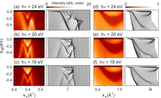
4 -0.4 1.0 -0.5 -0.4 -0.3 -0.2 -0.1 0.0 -0.5 -0.4 -0.3 -0.2 -0.1 0.0 -0.5 -0.4 -0.3 -0.2 -0.1 0.0 (a) h = 24 eV (b) h = 20 eV (c) h = 18 eV (d) h = 24 eV (e) h = 20 eV (f) h = 18 eV 0.4 0.0 0.4 k (Å )x -1 M E (eV) B 0.0 -0.2 -0.4 0.0 -0.2 -0.4 0.0 -0.2 -0.4
Intensity (arb. units)
0 20 0 1
k (Å )x -1
Figure 2.Surface and bulk band dispersion. ARPES intensity maps as a function of kx near ¯0 (a-c) and ¯M (d–f) and their corresponding EDCs, taken using
hν = 24, 20 and 18 eV photons. The intensity scale of (d–f) is a factor of about 20 smaller than that of (a–c) due to the intrinsic weakness of the ARPES signal near ¯M.
at kx ≈ −0.2 Å−1, outside the k range of the surface states near ¯0, and eventually splits into
two peaks. Such a strong kzdispersion, together with a broadened linewidth (1kx ≈ 0.12 Å−1),
is indicative of bulk band behavior, and indeed these MDC peaks trace out a Fermi surface (figure 1(d)) that is similar in shape to the hole pocket calculated for bulk Sb near H [23]. Therefore, by choosing an appropriate photon energy (e.g. 620 eV), the ARPES spectrum along ¯0– ¯M will have contributions only from the surface states. The small bulk electron pocket centered at L is not accessed using the photon energy range we employed (figure1(d)).
ARPES spectra along ¯0– ¯M taken at three different photon energies are shown in figure2. Near ¯0 there are two rather linearly dispersive electron-like bands that meet exactly at ¯0 at a binding energy EB∼ −0.2 eV. This behavior is consistent with previous ARPES measurements
along the ¯0– ¯K direction [13] and is thought to come from a pair of spin-split surface bands that becomes degenerate at the time reversal invariant momentum (TRIM) ¯0 due to Kramers degeneracy. The Fermi velocities of the inner and outer V-shaped bands are 4.4 ± 0.1 and 2.2 ± 0.1 eV Å, respectively, as found by fitting straight lines to their MDC peak positions. The surface origin of this pair of bands is established by their lack of dependence on hν (figures 2(a)–(c)). A strongly photon energy dispersive hole-like band is clearly seen on the negative kx side of the surface Kramers pair, which crosses EF for hν = 24 eV and gives rise
to the bulk hole Fermi surface near H (figure1(d)). For hν 6 20 eV, this band shows clear back folding near EB≈ −0.2 eV, indicating that it has completely sunk below EF. Further evidence
for its bulk origin comes from its close match to band calculations (figure2(a)). Interestingly, at photon energies such as 18 eV where the bulk bands are far below EF, there remains a uniform
envelope of weak spectral intensity near the Fermi level in the shape of the bulk hole pocket
5
seen with hν = 24 eV photons, which is symmetric about ¯0. This envelope does not change shape with hν, suggesting that it is of surface origin. Due to its weak intensity relative to states at higher binding energy, these features cannot be easily seen in the energy distribution curves (EDCs) in figures 2(a)–(c), but can be clearly observed in the MDCs shown in figure 1(c), especially on the positive kx side. Centered about the ¯M point, we also observe a
crescent-shaped envelope of weak intensity that does not disperse with kz (figures2(d)–(f)), pointing to
its surface origin. Unlike the sharp surface states near ¯0, the peaks in the EDCs of the feature near ¯M are much broader (1E ∼80 meV) than the spectrometer resolution (15 meV). The origin of this diffuse ARPES signal is not due to surface structural disorder because if that were the case, electrons at ¯0 should be even more severely scattered from defects than those at ¯M. In fact, the occurrence of both sharp and diffuse surface states originates from a k-dependent coupling to the bulk, as discussed later.
To extract the spin polarization vector of each of the surface bands near ¯0, we carried out spin-resolved MDC measurements along the ¯M0– ¯0– ¯M cut at E
B= −30 meV for maximal
intensity and used the two-step fitting routine developed in [24]. The Mott detector in the COPHEE instrument is mounted so that at normal emission it is sensitive to a purely out-of-plane spin component (z0) and a purely in-plane (y0) spin component that is rotated by 45◦ from the sample ¯0– ¯M direction (figure 3(a)). Each of these two directions represents a normal to a scattering plane, defined by the electron incidence direction on a gold foil and two detectors mounted on either side that measure the left–right asymmetry Ay0,z0= [(I
y0,z0
L −
IRy0,z0)/(ILy0,z0+ IRy0,z0)] of electrons backscattered off the gold foil [15]. Figure 3(d) shows the spin polarization for both components given by P = (1/Seff) × Ay
0,z0
, where Seff= 0.085 is the
Sherman function. Following the procedure described in [24], we take the spins to be fully polarized, assign a spin-resolved spectra for each of the fitted peaks Ii shown in figure 3(c) and fit the calculated polarization spectrum to the measurement. The spin-resolved spectra for the y-component derived from the polarization fit are shown in figure 3(e), given by Iy↑,↓=P4i =1Ii(1 ± Pyi)/6 + B/6, where B is a background and Pyi is the fitted y-component of polarization. There is a clear difference in Iy↑and Iy↓ at each of the four MDC peaks, indicating that the surface state bands are spin polarized. Each of the pairs l2/l1 and r1/r2 has opposite spin, consistent with the behavior of a spin-split Kramers pair, and the spin polarization of these bands is reversed on either side of ¯0 in accordance with time reversal symmetry (figure3(f)). Similar to Au(111) [21] and W(110)-(1×1)H [18], the spin polarization of each band is largely in-plane consistent with a predominantly out-of-plane electric field at the surface. However, unlike the case in Au(111), where the surface band dispersion is free electron like and the magnitude of the Rashba coupling can be quantified by the momentum displacement between the spin-up and spin-down band minima [21], the surface band dispersion of Sb(111) is highly non-parabolic. A comparison of the k-separation between spin-split band minima near ¯0 of Sb(111) (figure 3(b)) with those of Bi(111) [17], which are 0.03 and 0.08 Å−1, respectively,
nevertheless is consistent with the magnitude of the atomic p level splitting of Sb (0.6 eV) and Bi (1.5 eV) [25].
Figure4(a) shows the full ARPES intensity map from ¯0 to ¯M together with the calculated bulk bands of Sb projected onto the (111) surface. Although the sixfold rotational symmetry of the surface band dispersion is not known a pr i or i due to the threefold symmetry of the bulk, we measured an identical surface band dispersion along ¯0– ¯M’. The spin-split Kramers pair near ¯0 lies completely within the gap of the projected bulk bands near EF attesting
to their purely surface character. In contrast, the weak diffuse hole-like band centered near
6 0 -1 1 0 1 -1 0 1 -1 0 1 Px Py Pz Pin plane -0.2 -0.1 0.0 0.1 0.2 0.0 -0.1 -0.2 ’ E (eV) B (b) (a) || <111> 45 y’ x’ z’ x y z l2 l1 r1 r2 Intensity (arb. units) Polarizatio n (f) 0.0 -0.2 -0.4 0.2 0.4 P P y ’ z ’ -0.2 -0.1 0.0 0.1 0.2 Intensity (arb. units) 0.3 E = -30 meVB r2 r1 l1 l2 0 10 20 k (Å )x Intensity (arb. units) -0.2 -0.1 0.0 0.1 0.2 -1 E = -30 meVB 0 2 4 I I y y (e) (d) k (Å )x -1 -1 k (Å )x (c)
Figure 3. Large spin splitting of surface states on Sb(111). (a) Experimental geometry of the spin-ARPES study. At normal emission (θ = 0◦), the sensitive
y0-axis of the Mott detector is rotated by 45◦ from the sample ¯0– ¯M (k x)
direction, and the sensitive z0-axis of the Mott detector is parallel to the sample
normal. Spin up and down are measured with respect to these two quantization axes. (b) Spin-integrated ARPES spectra along the ¯M0– ¯0– ¯M direction taken
using a photon energy hν = 22 eV. The momentum splitting between the band minima is indicated by the black bar and is approximately 0.03 Å−1. (c) MDC
of the spin-integrated spectra at EB= −30 meV (shown in (b) by white line)
using a photon energy hν = 20 eV, together with the Lorentzian peaks of the fit. (d) Measured spin polarization curves (symbols) for the y0- and z0-components together with the fitted lines using the two-step fitting routine. Even though the measured polarization only reaches a magnitude of around ±0.4, similar to what is observed in thin film Bi(111) [20], this is due to a non-polarized background and overlap of adjacent peaks with different spin polarization. The fitted parameters are in fact consistent with 100% polarized spins. (e) Spin-resolved spectra for the y-component based on the fitted spin polarization curves shown in (d). (f) The in-plane and out-of-plane spin polarization components in the sample coordinate frame obtained from the spin polarization fit. The symbols refer to those in (c).
7 -0.6 -0.4 -0.2 0.0 0.2 Γ M M’ 0.2 0.0 -0.2 .0 0.0 0.2 0.0 -0.2 -0.4 -0.6 0.2 0.0 -0.2 -0.5 0.0 0.5 1.0 k (Å )x -1 k( Å) y -1 E (eV) B (a) (b) (d) Surface state FS Surface resonance FS Γ M Γ M (c) M
Figure 4. Topologically non-trivial surface states of Sb(111). (a) Calculated surface state band structure for freestanding 20 bilayer Sb(111) slabs together with an ARPES intensity map of Sb(111) along the ¯0– ¯M direction taken with hν = 22 eV photons. Green curves show the calculated bulk bands along the kx-direction projected onto the (111) plane. (b) ARPES intensity map at EF in
the kx–ky plane taken with hν = 20 eV photons. (c) Schematic picture showing
that the gapless spin-polarized surface bands (red and blue lines) connect the projected bulk valence and conduction bands (shaded regions) and are thus topologically non-trivial. The surface resonances (dashed green lines) do not connect the bulk valence and conduction bands and are thus topologically trivial. (d) Schematic diagram of the surface Fermi surface topology of Sb(111) showing the pockets formed by the pure surface states (unfilled) and the surface resonances (filled green). The purely surface state Fermi contours enclose only the single surface TRIM located at ¯0.
kx = 0.3 Å−1 and the electron-like band centered near kx = 0.8 Å−1 lie completely within the
projected bulk valence and conduction bands, respectively. Thus, their ARPES spectra exhibit the expected lifetime broadening due to hybridization with the underlying bulk continuum [26], a characteristic of surface resonance states. Figure4(b) shows the ARPES intensity plot at EFof
Sb(111) taken at a photon energy of 20 eV, where the bulk band near H is completely below EF
(figure2(b)). Therefore, this intensity map depicts the topology of the Fermi surface due solely to the surface states. By comparing figures4(a) and (b), we see that the innermost spin-polarized V-shaped band produces the circular electron Fermi surface enclosing ¯0, while the outer spin-polarized V-shaped band produces the inner segment (0.1 Å−16 k
x 6 0.15 Å−1) of the six-hole
Fermi surfaces away from ¯0. Previous ARPES experiments along the ¯0– ¯K direction [13] show that this outer V-shaped band merges with the bulk valence band; however, the exact value of kx
where this occurs along the ¯0– ¯M direction is unclear since only occupied states are imaged by ARPES. The outer segment of the six-hole pockets is formed by the hole-like surface resonance state for 0.15 Å−16 kx 6 0.4 Å−1. In addition, there are electron Fermi surfaces enclosing ¯M
and ¯M0 produced by surface resonance states at the BZ boundaries. Altogether, these results show that in a single surface BZ, the bulk valence and conduction bands are connected by a lone Kramers pair of surface states (figure4(c)).
8 Sb Bi0.9 0.1(111) 0.0 -0.2 k( Å) y -1 0.0 -0.2 -0.4 E (eV) B (b) k (Å )x -1 -0.6 k (Å )x -1 0.2 (a) 0.0 -0.4 0.4 0.0 0.4 0.8 M
Figure 5. Spin-split surface states survive alloying disorder in Sb0.9Bi0.1.
(a) ARPES intensity map at EF of single-crystal Sb0.9Bi0.1 (111) in the kx–ky
plane taken using 20 eV photons. (b) ARPES intensity map of Sb0.9Bi0.1 (111)
along the ¯0– ¯M direction taken with hν = 22 eV photons.
In general, the spin degeneracy of surface bands on spin–orbit coupled insulators can be lifted due to the breaking of space inversion symmetry. However, the Kramers theorem requires that they remain degenerate at four special TRIM on the 2D surface BZ, which for Sb(111) are located at ¯0 and three ¯M points rotated by 60◦ from one another. According to recent theory, there are a total of four Z2 topological numbersν0;(ν1ν2ν3) that characterize a 3D
spin–orbit-coupled insulator’s bulk band structure [3, 9, 11]. One in particular (ν0) determines whether
the spin-polarized surface bands cross EF an even or odd number of times between any pair of
surface TRIM and consequently whether the insulator is trivial (ν0= 0) or topological (ν0= 1).
An experimental signature of topologically non-trivial surface states in insulating Bi1−xSbx is
that the spin-polarized surface bands traverse EF an odd number of times between ¯0 and ¯M
[2,12,19]. Although this method of counting cannot be applied to Sb because it is a semimetal, since there is a direct gap at every bulk k-point, it is meaningful to assume some perturbation, such as alloying with Bi [27] that does not significantly alter the spin splitting (figure 5), that pushes the bulk valence H and conduction L bands completely below and above EF, respectively,
without changing its Z2class. Under such an operation, it is clear that the spin-polarized surface
bands must traverse EFan odd number of times between ¯0 and ¯M, consistent with the 1;(111)
topological classification of Sb. This conclusion can also be reached by noting that the spin-split pair of surface bands that emerge from ¯0 does not recombine at ¯M, indicative of a ‘partner switching’ [9] characteristic of topological insulators.
In conclusion, we have mapped the spin structure of the surface bands of Sb(111) and shown that the purely surface bands located in the projected bulk gap are spin split by a combination of spin–orbit coupling and loss of inversion symmetry at the crystal surface. The spin-polarized surface states have an asymmetric Dirac-like dispersion that gives rise to its k-splitting between spin-up and spin-down bands at EF. This property of Sb, in
combination with its small density of spin degenerate bulk states at the Fermi level due to its semimetallic nature, makes it a promising candidate for high-temperature spin current sources. Moreover, its topologically non-trivial surface band structure makes Sb(111) an especially appealing candidate for an unusual 2D Dirac protected free fermion system that exhibits antilocalization [9].
9
Acknowledgments
We thank C L Kane for theoretical discussions. References
[1] Kane C L and Mele E J 2005 Phys. Rev. Lett.95 146802
[2] Hasan M Z and Kane C L 2010 Rev. Mod. Phys.82 3045
[3] Moore J E and Balents L 2007 Phys. Rev. B75 121306
[4] Kane C L and Mele E J 2005 Phys. Rev. Lett.95 226801
[5] Bernevig B A et al 2006 Science314 1757
[6] König M et al 2008 J. Phys. Soc. Jpn.77 031007
[7] Haldane F D M 1988 Phys. Rev. Lett.61 2015
[8] Wu C et al 2006 Phys. Rev. Lett.96 106401
[9] Fu L et al 2007 Phys. Rev. Lett.98 106803
[10] Murakami S 2007 New J. Phys.9 356
[11] Roy R 2009 Phys. Rev. B79 195321
[12] Hsieh D et al 2008 Nature452 970
[13] Sugawara K et al 2006 Phys. Rev. Lett.96 046411
[14] Höchst H and Ast C R 2004 J. Electron Spectrosc. Relat. Phenom.137 441
[15] Hoesch M et al 2002 J. Electron Spectrosc. Relat. Phenom.124 263
[16] Bengió S et al 2007 Surf. Sci.601 2908
[17] Koroteev Y M et al 2004 Phys. Rev. Lett.93 046403
[18] Hochstrasser M et al 2002 Phys. Rev. Lett.89 216802
[19] Teo J, Fu L and Kane C L 2008 Phys. Rev. B78 045426
[20] Hirahara T et al 2007 Phys. Rev. B76 153305
[21] Hoesch M et al 2004 Phys. Rev. B69 241401
[22] Gonze X et al 1991 Phys. Rev. B44 11023
[23] Falicov L M and Lin P J 1965 Phys. Rev.141 562
[24] Meier F et al 2008 Phys. Rev. B77 165431
[25] Liu Y and Allen E 1995 Phys. Rev. B52 1566
[26] Kneedler E, Smith K E, Skelton D and Kevan S D 1991 Phys. Rev. B44 8233
[27] Lenoir B et al 1996 15th Int. Conf. on Thermoelectrics (Pasadena, CA) (New York: IEEE) p 113