HAL Id: cea-01803825
https://hal-cea.archives-ouvertes.fr/cea-01803825
Submitted on 10 Jan 2019
HAL is a multi-disciplinary open access archive for the deposit and dissemination of sci-entific research documents, whether they are pub-lished or not. The documents may come from teaching and research institutions in France or abroad, or from public or private research centers.
L’archive ouverte pluridisciplinaire HAL, est destinée au dépôt et à la diffusion de documents scientifiques de niveau recherche, publiés ou non, émanant des établissements d’enseignement et de recherche français ou étrangers, des laboratoires publics ou privés.
Transient current induced in thin film diamonds by swift
heavy ions
Shin-Ichiro Sato, Takahiro Makino, Takeshi Ohshima, Tomihiro Kamiya,
Wataru Kada, Osamu Hanaizumi, Veljko Grilj, Natko Skukan, Michal
Pomorski, Gyorgy Vizkelethy
To cite this version:
Shin-Ichiro Sato, Takahiro Makino, Takeshi Ohshima, Tomihiro Kamiya, Wataru Kada, et al.. Tran-sient current induced in thin film diamonds by swift heavy ions. Diamond and Related Materials, Elsevier, 2017, 75, pp.161-168. �10.1016/j.diamond.2017.04.005�. �cea-01803825�
Title:
Transient Current Induced in Thin Film Diamonds by Swift Heavy Ions
Authors:
Shin-ichiro Satoa,*, Takahiro Makinoa, Takeshi Ohshimaa, Tomihiro Kamiyaa, Wataru Kadab, Osamu Hanaizumib, Veljko Griljc, Natko Skukanc, Ivan Sudićc, Milko Jakšićc, Michal Pomorskid, Gyorgy Vizkelethye*
Affiliation:
a
Quantum Beam Science Research Directorate (QuBS), National Institutes for Quantum
and Radiological Science and Technology (QST), Takasaki, Gunma 370-1292, 370-1292
b
Division of Electronics and Informatics, Faculty of Science and Technology, Gunma
University, Kiryu, Gunma 376-8515, Japan
c
Division for Experimental Physics, Ruđer Bošković Institute (RBI), 10000 Zagreb,
Croatia
d
CEA-LIST, Diamond Sensors Laboratory, Gif-sur-Yvette F-091191, France
e
Sandia National Laboratories (SNL), P.O. Box 5800, Albuquerque, NM 87185-1056,
USA
Corresponding Author: Shin-ichiro Sato (S-I. Sato)
Tel: +81-27-346-9378; E-mail: sato.shinichiro2@qst.go.jp
*
Sandia National Laboratories is a multi-program laboratory managed and operated by Sandia Corporation, a wholly owned subsidiary of Lockheed Martin Corporation, for the U.S. Department of Energy’s National Nuclear Security Administration under contract DE-AC04-94AL85000.
Key Words:
Diamond crystal, radiation induced effects, detectors, membranes
Abstract
Single crystal diamond is a suitable material for the next generation particle detectors
because of the superior electrical properties and the high radiation tolerance. In order to
clarify fundamental characteristics of diamond particle detectors, transient currents
generated in diamonds by single swift heavy ions (26 MeV O5+ and 45 MeV Si7+) were investigated. Two dimensional mappings of transient currents by single ion hits were also
measured. In the case of 50 µm-thick diamond, both the signal height and the collected
charge were reduced by the subsequent of ion hits and the charge collection time was
extended. Strong signals appeared occasionally when most of the signals were fully
degraded. These results were thought to be attributable to the polarization effect in
diamond and it appeared only at the positive bias. In the case of 6 µm-thick diamond
membrane, an “island” structure was found in the 2D mapping of transient currents.
Signals in the islands showed different applied bias dependence from signals in other
regions, indicating different crystal quality. The instability of signals resulting from the
polarization effect was also observed in the 6 µm-thick diamond membrane. Simulation
study of transient currents based on the Shockley-Ramo theorem clarifies that the
polarization appears only in the irradiated region and both the electric field and the hole
1. Introduction
Diamond is an attractive material for radiation detectors to be used in harsh environments
because of its superior electronic properties, such as high carrier mobility, wide bandgap,
high radiation tolerance, and high breakdown voltage. Although the study for diamond
radiation detectors started in the 1940s [1, 2], many problems about the sample
preparation, such as availability, crystal quality, and control of impurity, made the
development difficult because natural diamonds were used in the earliest years. Since
significant improvement has been recently achieved in the crystal growth technology of
diamond, research and development for single-crystal diamond radiation detectors has
been extensively carried out in recent years and their superior characteristics has been
demonstrated [3]. For instance, it has been recently reported that single-crystal diamonds
grown by chemical vapor deposition (CVD) showed almost 100 % charge collection
efficiency and high energy resolution (less than 1 %) in the detection of 5.486 MeV alpha
particles from 241Am [4].
With the development of research on diamond particle detectors, however, some issues
has also come out. One of the critical issues on diamond particle detectors is the
polarization effect: temporal degradation of signal amplitude during ion irradiation. Being
generally known to occur in insulator crystals [5], the polarization effect has been one of
disappears by changing the polarity of applied bias and occasionally mitigated during ion
irradiation [9]. This is more pronounced for short range ions, which produce high
ionization in a small volume [10]. When charge carriers generated by radiation are trapped
in deep levels in diamond, they cannot be released in a short time and give rise to a space
charge (internal electric field). The external electric field is screened by the space charge
and as a result, the collected charge signal amplitude decreases. This is a brief explanation
of the polarization effect, and the detail mechanism is still less well understood. The origin
of these deep levels is completely unidentified. It is also still unclear how the charge
collection process of generated carriers are affected by the polarization effect.
In this study, transient currents in diamond generated by swift heavy ions were measured
using Time Resolved Ion-Beam Induced Current (TRIBIC) technique [11] in order to
investigate the charge collection process in diamonds. The TRIBIC technique is a
powerful tool for investigating the collection process of generated charge by incident ions.
Two dimensional distribution of transient currents was also investigated.
2. Experimental
Two samples were used in this study: a single-crystal CVD (sc-CVD) diamond with the
thickness of 50 µm and a thin sc-CVD diamond membrane with the thickness of 6 µm.
The fabrication method of diamond membrane was reported elsewhere [12]. The
detectors were of electrical grade (substitutional nitrogen content [N] < 5 ppb) and optical
grade ([N] < 5 ppm), respectively, which were commercially available from Element Six
generated by incident ions (26 MeV O5+ and 45 MeV Si7+). Current-voltage (IV) and capacitance-voltage (CV) characteristics were investigated prior to TRIBIC
measurements.
The experimental setup of TRIBIC measurement is illustrated in Fig. 1. Comparing to
conventional Ion Beam Induced Charge (IBIC) technique [13], the TRIBIC measurement
gives information on time variation of charge collection, i.e. transient current, in addition
to generated charge by a single ion incidence. The detail of TRIBIC measurement system
was reported elsewhere [11]. The samples were irradiated at normal incidence with a
focused microbeam of 26 MeV O5+ and 45 MeV Si7+ ions at the Sandia National Laboratories (SNL), USA. Ion-induced transient currents generated by single ion hits
were measured from the top electrode of sample by the 20 GHz oscilloscope (Tektronix,
DPO 72004) via a linear amplifier (Picosecond Pulse Labs, 5840B) and a bias tee. The
transient currents and their positional information were measured, and the two
dimensional (2D) mapping of the transient currents was recorded. The spot size of the
microbeam was about 1 µm in diameter. The microbeam was scanned from left to right
and from bottom to top, and the scan area was 50×50 µm2. A bias voltage ranging from -50 V to +-50 V was applied to the top electrode of sample (the same side as ion incidence)
and the bottom electrode was grounded. The variation of transient currents due to applied
bias voltages was also investigated.
Energy depositions and creation of number of electron-hole pairs by incident ions were
calculated by SRIM [14]. The calculation results are shown in Fig. 2. The projected ranges
respectively. Therefore, 45 MeV-Si ions completely pass through the 6 µm-thick diamond
membrane and 38.9 MeV (86.4%) of the energy was estimated to be deposited by
electronic excitation. The diamond density of 3.515 g/cm3 and the average ionization (electron-hole pair creation) energy of 13.2 eV [15] were used in these calculations.
Fig. 1. Experimental setup of TRIBIC measurement.
0 2 4 6 8 10 0 2 4 6 8 10 Ionization (keV/ µ m) Depth (µm) 26 MeV-O 45 MeV-Si Implanted Ion Distribution
Fig. 2. Implanted ion distributions and deposited energy profiles of 26 MeV Oxygen and 45 MeV
Silicon into diamond.
3. Results and Discussion
3.1. TRIBIC signals of 50 µm-thick diamond
Figure 3 shows the IV characteristics of the 50 µm-thick diamond. Although the IV
characteristics indicates that the Ohmic contacts were incompletely formed, the
capacitance was 5.35 pF independent of the bias voltage. Therefore, a uniform external
electric field by the bias supply was formed throughout the diamond between the top and
bottom electrodes.
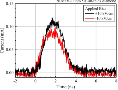
Figure 4 shows typical transient currents (TRIBIC signals) at the biases of ±50 V (±10
kV/cm) when a single 26 MeV-O ion hit to the 50 µm-thick diamond. The linear amplifier
was not used for this measurement. The signals at the positive bias were larger than the
signals at the negative bias and no significant difference was observed in the width of
signal. Collected charge was obtained by integrating transient current with respect to time
and charge collection efficiency (CCE) was also obtained from the collected charge, the
deposited ion energy, and the average ionization energy. Thecharge generated in 50
µm-thick diamond by 26 MeV Oxygen was estimated to be 0.318 pC. Figure 5 shows
variations of the peak heights and CCEs of TRIBIC signals as a function of applied
electric field. Both the peak height and the CCE increased with increasing absolute value
86.2 % at +10 kV/cm and 60.4 % at -10 kV/cm. This trend corresponds to the results
reported elsewhere [4, 10]. According to the Shockley-Ramo theorem [16], in the case of
charge generation near one electrode, CCE as a function of applied electric field can be
explained by a single-carrier Hecht equation:
CCE = $% &
' 1 − exp −
'
$% & (1).
Where W, E, and µτ are the thickness, the electric field, and the mobility-lifetime product,
respectively. A uniform electric field in the diamond is assumed in Eq. (1). The fitting
result is shown as the red line in Fig. 5. The values of µt product were (1.8±0.2)×10-6 cm2/V for holes and (6.4±0.8)×10-7 cm2/V for electrons. These values are substantially lower than the values reported elsewhere [4, 10, 17, 18] which can be explained as follows.
Firstly, since density of electron-hole pairs generated by swift heavy ions is much higher
than that of light ions like protons and alpha particles, some carriers recombine promptly
after generation, the value of CCE for swift heavy ions are generally lower than that for
light ions [19]. As a result, the lower value of µτ product was obtained from the CCE for
heavy ions than the reported values. Also, since we performed irradiation experiments
using this sample prior to this study, significant radiation degradation might have been
Fig. 3. Current-voltage characteristics of the 50 µm-thick diamond. Negative values in current were
converted to the positive values in order to show in the semi-logarithmic scale.
-2 0 2 4 6 8 0.00 0.05 0.10 0.15 Current (mA) Time (ns) Applied Bias +10 kV/cm -10 kV/cm 26 MeV-O into 50 µm-thick diamond
Fig. 4. Typical TRIBIC signals of the 50 µm-thick diamond generated by a single 26 MeV O5+ ion hit. The applied electric fields were +10 kV/cm (black) and -10 kV/cm (red). The linear amplifier was not used for this measurement.
-10 -5 0 5 10 0.00 0.03 0.06 0.09 0.12 0.15
Peak Height (mA)
Electric Field (kV/cm) Peak height
26 MeV-O into 50 µm-thick diamond
0 20 40 60 80 100 CCE
Fit for CCE
CCE (%)
Fig. 5. Variations of peak height of TRIBIC signal (closed squares) and charge collection efficiency
(CCE, red open circuits) of the 50 µm-thick diamond due to 26 MeV O5+ ion hits as a function of electric field. The line in red are the fitting curve of CCE by Eq. (1).
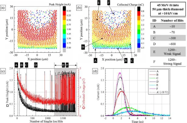
Fig. 6. (a) Two dimensional maps of peak height of TRIBIC signals and (b) collected charge induced
µm2. (c) Variations of the peak height (black) and the collected charge (red) as a function of number of single ion hits. (d) TRIBIC signals at the positions of A to F shown in (b). The number of hits at A to F are listed in the right table. A typical TRIBIC signal at the bias of -50 V (-10 kV/cm) is also shown in (d).
The TRIBIC measurement results of the 50 µm-thick diamond by 45 MeV Si7+ ion hits at +10 kV/cm are summarized in Fig. 6. Since the linear amplifier was used, the signal
heights were much larger than the signals by 26 MeV O5+ ions in Fig. 4. Figs. 6(a) and (b) show the 2D maps of signal heights and collected charges of TRIBIC signals,
respectively. Fig. 6(c) shows the variation of peak heights and collected charge as function
of number of single ion hits. Fig. 6(d) shows typical TRIBIC signals at different XY
positions and also the typical TRIBIC signal at -10 kV/cm (dashed line in black). These
signals are identified by the letters of A to F and A’, and their XY positions and the number
of hits are shown in Figs. 6(b) and (c), respectively. These data were obtained by taking
the average of ten TRIBIC signals around the number of hits shown in the table in the
upper right of Fig. 6.
It was found from Fig. 6(c) that both the signal height and the collected charge decreased
gradually with increasing number of hits. The increase in the width of the transient current
in addition to the decrease in peak height appeared (see the signals A, B, C, and D in (d)).
The microbeam was scanned from left to right, and from bottom to top, and the transient
current was recorded only when the signal height was higher than a trigger level of the
oscilloscope. Therefore, the signal amplitude was reduced gradually from the bottom left
to the top right in the 2D maps and eventually the signal height fell below the trigger level.
the upper region of 2D maps. Since a saturation tendency of decrease in TRIBIC signal
which was observed after ~1000 hits was just due to the trigger level, the actual signal
amplitude would continue to decrease after ~1000 hits. However, interestingly, strong
signals appeared sparsely at the upper region of 2D mapping (after ~1200 hits, see the
shaded zone in (c)). The typical weak and strong TRIBIC signals were shown as the
signals E and F in (d). The shape of signals E and F was unchanged from signals D and
A, respectively.
These results are obviously attributable to the polarization effect. When ion induced
carriers (electrons and holes) are trapped in deep levels in diamond, the trapped carriers
interfere with the external electric field and the charge collection is interrupted. The detail
of polarization effect is discussed in section 3.3. We therefore conclude that the
inhomogeneous 2D maps in Figs. 6(a) and (b) do not indicate the inhomogeneity of crystal
quality, but are simply caused by enhancing the polarization effect with increasing
number of ion hits. The results of Fig. 6 also indicate that the polarization effect induced
by previous ion hits are widely spread bidimensionally and the degradation of signal
amplitude occurs even if the position of subsequent ion hits is different from that of
precedent ion hits. The spatial distribution of the polarization effect could be estimated to
be over the range of microns, although it is difficult to estimate the exact value in this
study.
The strong signal F occasionally observed after 1200 hits were comparable to the signal
before the polarization occurred (the signal A), and the weak signals (the signal E)
polarization effect was temporarily cleared out by excess accumulation of carriers due to
the repetition of ion hits [9]. On the other hand, the polarization effect is
polarity-dependent and the inhomogeneous mapping was never observed when the negative bias
was applied. Also, the signal height at -10 kV/cm, which is shown as the signal A’ in Fig.
6(d), was about 60% compared to the signal at +10 kV/cm.
3.2. TRIBIC signals of 6µm-thick diamond membrane
The TRIBIC signals of the 6 µm-thick diamond membrane by 45 MeV Si7+ ion hits are summarized in Fig. 7. Figures 7(a) and (b) show the 2D maps of peak height of TRIBIC
signals at the biases of -3 V (-5 kV/cm) and +3 V (+5 kV/cm), respectively. The 2D maps
of collected charges are not shown here since they were qualitatively no different from
that of peak heights. The ion irradiation at a strong positive bias (+50 kV/cm) was
performed just before the TRIBIC measurements and “island” structure appeared in the
2D map. Examples of TRIBIC signals at ±5 kV/cm are shown in (c) and (d), respectively.
These signals are identified by the letters of G to K and their locations are listed in the
table in Fig. 7. Figures 7(d) and (e) show the histograms of peak height and collected
charge, respectively.
At the negative bias condition (Fig. 7(c)), the signals at the islands (the signal G) were
stronger than the signals at the other region (the signal H). Meanwhile, at the positive bias
condition (Fig. 7(d)), the signals at the other region (the signal K) were stronger than that
at the islands (the signal I). In addition, the weaker signals were found at the coast of
islands (the signal J). The signals at the other region appeared sparsely, indicating most
and could not be detected by the oscilloscope. The signal height at the other region at -5
kV/cm (the signal H) was about 60% compared to +5 kV/cm (the signal K).
The trend observed at the other region is very similar to the result of Fig. 6, indicating the
polarization effect could also appear in the 6 µm-thick diamond membrane. Although the
polarization effect has been often observed in diamond whose thickness is considerably
longer than projected range of ions, swift heavy ions which have high electronic energy
deposition can induce the polarization effect even if diamond is thin enough for ions to
penetrate. On the other hand, the signals at the islands showed a different trend from the
other region, suggesting the existence of dislocation, inclusion, or grain boundary. The
difference of bias polarity dependence is thought to be due to the difference of crystal
quality in the islands. It is unclear at the present stage whether the island structure was
formed during crystal growth or during the RIE etching for the fabrication of membrane
Fig. 7. Summary of TRIBIC data in the 6 µm-thick diamond membrane due to 45 MeV Si7+ ion hits at ±5 kV/cm. (a) and (b) show the 2D maps of the peak heights at -5 kV/cm and +5 kV/cm, (c) and (d) show typical transient currents at -5 kV/cm and +5 kV/cm, respectively. (e) and (f) are histograms of the peak height and the collected charge, respectively.
3.3. Analysis of the polarization effect based on the Shockley-Ramo theorem
In order to analyze the signal degradation due to the polarization effect shown in Fig. 6(d),
a simulation of transient currents based on the Shockley-Ramo theorem developed by Li
et al. [20] was performed. A one-dimensional model of charge collection in
semiconductors can be obtained from the Shockley-Ramo theorem and this is suitable to
clarify how the polarization effect affects the charge collection process. Figure 8(a) shows
the conceptual diagram of the model proposed in this study. It was assumed that an electric
field was formed uniformly in diamond and the polarization occurred only in the
irradiated region. In this case, the transient current, i(t), is represented by the following
equations: 𝑖 𝑡 = 𝑖/ 𝑡 + 𝑖1 𝑡 (2) 𝑖/ 𝑡 = 2 3'exp − 5 %6 Λ 𝑥, 𝑡 ∙ 𝑣/ 𝑥 ' < 𝑑𝑥 (3) 𝑖1 𝑡 = 2 3' Λ 𝑥, 𝑡 ∙ 𝑣1 𝑥 ∙ exp − 5 %>? @ < 𝑑𝑥 + Λ 𝑥, 𝑡 ∙ 𝑣1 𝑥 ∙ exp − 5 %>A ' @ 𝑑𝑥 (4).
Where ie(t), ih(t), and t denote the electron current, the hole current, and the time,
respectively. q, Λ, G, R, and W are the electron charge, the electronic energy deposition
by incident ions, the average ionization energy (13.2 eV [15]), projected range of incident
ions, and the sample thickness. The data of Λ(x, t = 0) was obtained from Fig. 2. The
hand, it was assumed that the hole lifetime in the irradiated region (0 ≤ 𝑥 ≤ 𝑅), τh1 was
reduced by the polarization effect and the hole lifetime in the other region (R< 𝑥 ≤ 𝑊),
τh2 was unchanged. The drift velocity, v is represented by the Canali model [21]:
𝑣H = $I& J
KLMIN O
PQI
𝑖 = 𝑒, ℎ (5).
Where µ, vs, and E are the drift mobility, the saturation velocity, and the electric field. The
subscripts, e and h denote electron and hole, respectively Constant values were used for
both the electron and the hole mobilities, and the drift velocity was changed only by the
change in electric field. Values of 1.5×107 cm/s and 1.05×107 cm/s were used for electron and hole saturation velocity [2]. Finally, the calculated current was convolved with a
Gaussian that included all terms of the system resolution, such as stray capacitance, etc.
The typical response time was 6.5×10⁻¹⁰ s for the 50 µm-thick diamond and 3.0×10⁻¹⁰ s for the 6 µm-thick diamond membrane.
Initial values of mobility and lifetime were determined from fittings of the signals A and
A’ in Fig. 6(d), which were the transient currents without polarization. The obtained
values are summarized in Table 1 and the fitting results are shown in Fig. 8(b). The
products of mobility and lifetime for electrons and holes in Table 1 were slightly smaller
than the µτ products which were obtained in Fig. 5. This is attributed to the difference of
incident ions [19].
Table 1. Parameters used for the simulation of transient currents in Fig. 6(d).
Electron mobility, µe (cm 2 /Vs) 2.2×10² Hole mobility, µh (cm 2 /Vs) 3.1×10²
Electron lifetime, τe (ns) 2.4
Hole lifetime, τh1 (ns) 5.45
Hole lifetime after polarization, τh2 (ns) 1.1 Electric field after polarization, Ep (V/cm) 5.0×10
2
Although the polarization effect simply induces the reduction of electric field in diamond
according to the general understanding, it was shown from the simulation study that the
decrease in hole lifetime should also be taken into account to fit degraded transient
currents after the polarization. Assuming both the electric field and the hole lifetime are
reduced by the polarization effect only in the irradiated region (0 ≤ 𝑥 ≤ 𝑅), transient
currents were calculated and the results for the 50-µm thick diamond are illustrated in Fig.
8(b). In Fig. 8(b), the experimental transient currents as well as the calculated results are
shown. The signal D, which is the transient current after the polarization, could be
simulated by considering both the decrease in hole lifetime and electric field in the
irradiated region. The results showed the hole lifetime and the electric field were reduced
from 5.45 ns and +10 kV/cm and to 1.1 ns and +0.50 kV/cm, respectively.
This model also explains well the transient currents in the 6-µm thick diamond membrane.
45 MeV-Si ions completely penetrate the 6-µm diamond membrane and induce the
polarization, i.e. the decrease in both electric field and hole lifetime, throughout the depth
direction. In this case, however, the electron current is comparable with the hole current
and we were unable to determine individual parameters for electrons and holes. Therefore
the same parameters were used for electrons and holes to simulate the signal K. The
agreement with the signal J when the electric field and hole lifetime were reduced from
+5.0 kV/cm and 5.0 ns to +2.0 kV/cm and 3.0 ns, respectively. Further discussion should
be conducted for the change in electron lifetime in the irradiated region, although no
variation of electron lifetime was assumed in this study. Since the polarization effect is
observed at the condition of positive bias only, it is difficult to discuss the existence of
Fig. 8. (a) One-dimensional model of the polarization effect based on the Shockley-Ramo theorem.
(b) and (c) are calculation results of the 50 µm-thick diamond (red lines) and the 6 µm-thick diamond membrane (blue lines), respectively. Electron and hole currents are drawn as the dashed and dashed-dotted lines, respectively.
4. Conclusion
Transient currents (TRIBIC signals) of diamonds induced by single swift heavy ion hits
and their 2D mappings were investigated in this study. Variations of TRIBIC signals and
CCEs due to different diamond thicknesses, applied biases, and bias polarities were
clarified. Change in the TRIBIC signals by subsequent of ion hits was also investigated.
From the results of TRIBIC measurements in the 50 µm-thick diamond by irradiated by
45 MeV-Si ions, the signal degradation and instability originating from the polarization
effect were observed. At positive bias, signals were drastically degraded by the
subsequent ion hits and became unstable with increasing number of ion hits. An increase
in the charge collection time in addition to the decrease in signal height were observed.
After 1200 ion hits, non-degraded signals appeared occasionally with fully degraded
signals. The spatial distribution of the polarization effect could be estimated to be in the
range of microns. At negative bias, on the other hand, neither signal degradation nor
instability of TRIBIC signals appeared with the subsequent of ion hits. The signal height
at negative bias was about 60% compared to the signal height at positive bias.
The similar trend was found in the TRIBIC results of the 6 µm-thick diamond membrane
by 45 MeV-Si ion hits. This fact strongly indicates that the polarization effect could occur
in diamond membranes by swift heavy ions. Island structure was found in the 2D maps
and signals in the islands showed different trend from the other regions. The
inhomogeneity is thought to be caused by the presence of dislocation, inclusion or grain
Also, simulation study based on the Shockley-Ramo theorem was performed to
understand the observed polarization effect. The proposed model explains well transient
currents in both thick and thin diamond. It was shown from the simulation study that the
polarization occurred only in the irradiated region and induced significant reduction of
hole lifetime in addition to electric field.
Acknowledgement
This work was supported by JSPS KAKENHI Grant Number 26249149. Sandia National
Laboratories is a multi-program laboratory managed and operated by Sandia Corporation,
a wholly owned subsidiary of Lockheed Martin Corporation, for the U.S. Department of
Energy’s National Nuclear Security Administration under contract
DE-AC04-94AL85000.
References
[1] S. F. Kozlov, E. Belcarz, M. Hage-Ali, R. Stuck, and P. Siffert, Nucl. Instr. Meth. 117
(1974) 277-283.
[2] F. Nava, C. Canali, M. Artuso, E. Gatti, P. F Manfredi, and S. F. Kozlov, IEEE Trans.
Nucl. Sci. NS-26 (1979) 308-315.
[3] For example: V. Grilj, N. Skukan, M. Pomorski, W. Kada, N. Iwamoto, T. Kamiya, T.
Ohshima, and M. Jakšić, Appl. Phys. Lett. 103 (2013) 243106-1-4.
[4] M. Tsubota, J. H. Kaneko, D. Miyazaki, T. Shimaoka, K. Ueno, T. Tadokoro, A.
(2015) 50-56.
[5] S. F. Kozlov, R. Stuck, M. Hage-Ali, and P. Siffert, IEEE Trans. Nucl. Sci. NS-22
(1975) 160-170.
[6] W. Kada, N. Iwamoto, T. Satoh, S. Onoda, V. Grilj, N. Skukan, M. Koka, T. Ohshima,
M. Jakšić, and T. Kamiya, Nucl. Instr. Meth. B 331 (2014) 113-116.
[7] Y. Sato and H. Murakami, Jpn. J. Appl. Phys. 4 (2015) 096401-1-5.
[8] G. Gervino, S. Bizzaro, C. Palmisano, and L. Periale, Nucl. Instr. Meth. A 718 (2013)
325-326.
[9] Y. Sato, T. Shimaoka, J. H. Kaneko, H. Murakami, M. Isobe, M. Osakabe, M. Tsubota,
K. Ochiai, A. Chayahara, H. Umezawa, and S. Shikata, Nucl. Instr. Meth. A 784 (2015)
147-150.
[10] V. Grilj, N. Skukan, M. Jakšić, W. Kada, and T. Kamiya, Nucl. Instr. Meth. B 306
(2013) 191-194.
[11] H. Schone, D. S. Walsh, F. W. Sexton, B. L. Doyle, P. E. Dodd, J. F. Aurand, R. S.
Flores, and N. Wing, IEEE Trans. Nucl. Sci. 45 (1998) 2544-2549.
[12] M. Pomorski, B. Caylar, and P. Bergonzo, Appl. Phys. Lett. 103 (2013) 112106-1-4.
[13] M. B. H. Breese, E. Vittone, G. Vizkelethy, and P. J. Sellin, Nucl. Instr. Meth. B 264
(2007) 345-360.
[14] Available at: <http://www.srim.org>
[15] C. Canali, E. Gatti, S. F. Kozlov, P. F. Manfredi, C. Manfredotti, F. Nava, and A.
Quirini, Nucl. Instr. Meth. 160 (1979) 73-77.
[16] E. Vittone, F. Fizzotti, A. Lo Giudice, C. Paolini, C. Manfredotti, Nuc. Instr. Meth.
B 161 (2000) 446-451.
R. Edwards, Appl. Phys. Lett. 90 (2007) 102111-1-3.
[18] A. Galbiati, S. Lynn, K. Oliver, F. Schirru, T. Nowak, B. Marczewska, J. A. Dueñas,
R. Berjillos, I. Martel, and L. Lavergne, IEE Trans. Nucl. Sci. 56 (2009) 1863-1874.
[19] T. Ohshima, N. Iwamoto, S. Onoda, G. Wagner, H. Itoh, and K. Kawano, Surf. Coat.
Tech. 206 (2011) 864-868.
[20] Z. Li and H. W. Kraner, Nuclear Physics B (Proc. Suppl.) 32 (1993) 398-409.
[21] C. Canali, G. Majini, R. Minder, and G. Ottaviani, IEEE Trans. Electron Dev. 22