HAL Id: hal-01986656
https://hal.archives-ouvertes.fr/hal-01986656
Submitted on 14 Mar 2019
HAL is a multi-disciplinary open access
archive for the deposit and dissemination of
sci-entific research documents, whether they are
pub-lished or not. The documents may come from
teaching and research institutions in France or
abroad, or from public or private research centers.
L’archive ouverte pluridisciplinaire HAL, est
destinée au dépôt et à la diffusion de documents
scientifiques de niveau recherche, publiés ou non,
émanant des établissements d’enseignement et de
recherche français ou étrangers, des laboratoires
publics ou privés.
Towards simulation at picometer-scale resolution:
Revisiting inversion domain boundaries in GaN
Frédéric Lançon, Luigi Genovese, J. Eymery
To cite this version:
Frédéric Lançon, Luigi Genovese, J. Eymery.
Towards simulation at picometer-scale resolution:
Revisiting inversion domain boundaries in GaN. Physical Review B: Condensed Matter and
Ma-terials Physics (1998-2015), American Physical Society, 2018, 98 (16), pp.165306.
�10.1103/Phys-RevB.98.165306�. �hal-01986656�
Towards simulation at picometer-scale resolution:
revisiting inversion domain boundaries in GaN
Fr´ed´eric Lan¸con,1, ∗ Luigi Genovese,1 and Jo¨el Eymery1
1
Univ. Grenoble Alpes (UGA), INAC-MEM, F-38000 Grenoble, France CEA, INAC-MEM, L Sim, F-38054 Grenoble, France
(Dated: March 1, 2019)
Motivated by recent high resolution results on the inversion domain boundaries (IDB) in gallium nitride, we refine by ab initio DFT calculations the well established atomic model IDB∗ derived by Northrup et al. This allows us to recover these experimental results obtained by coherent x-ray diffraction and showing small additional shifts of the polarity domains, in particular 8 pm shift along the hexagonal direction. The influence of boundary conditions and electrostatic fields (IDB-IDB and IDB-surface interactions) on the results and the existence of metastable solutions is carefully discussed to stress the accuracy of the method. These results demonstrate a cross-talk between advanced characterization tools and state-of-the-art ab initio calculations that opens perspectives for the structural analysis of defects in the picometer range.
Introduction — Precision in DFT calculations for solid-state physics has been recently studied1 and a very good reproducibility of the results has been reported among several current codes. For instance, a repro-ducibility of 1 pm has been found on the different cal-culated lattice parameters of silicon. Yet, this precision obtained in the calculation corresponds to an accuracy of 6 pm with respect to the experimental value1. We intend
here to get a better agreement in the accuracy of geo-metrical characteristics of gallium nitride, a widely stud-ied compound of technological importance. Challenged by recent experimental results2 on very common planar defects in GaN material, we have conducted a detailed analysis of them. Gallium-nitride crystal is a wurtzite-like structure, i.e. a hexagonal lattice with one fourth of the Ga–N bonds oriented along the hexagonal-symmetry axis. Inversion domain boundaries (IDB) are interfaces between crystalline polarity domains, which can be noted −c and +c. These domains have their hexagonal axis in common, but have opposite orientations for their Ga– N bonds parallel to it. By convention, in +c domains these Ga → N bonds are oriented along [0 0 0 1] of the material, while it is [0 0 0 ¯1] for −c domains. Depend-ing on the experimental conditions, a given type of do-main is usually preferably produced during the crystal growth. The growing surface perpendicular to [0 0 0 1] is either Ga terminated for +c domains or N terminated for −c. However, both domain types separated by IDB frequently coexist in thin films3–7and in wires8,9. It usu-ally corresponds to detrimental defects in the materials, but periodic alternation of domains is garnering interest in a wide range of devices such as those for non linear frequency conversion10–12.
IDB structures are usually studied by electron microscopy3–5,7,9,13. These studies confirm the
pioneer-ing model for IDB∗ introduced by Northrup et al14, who
determined its structure and stability with ab initio DFT
calculations. This model gets the lowest energy of possi-ble structures by keeping hetero first-neighbor bonds at the cost of some bond-angle distortions at the boundary. It provides a characteristic shift of the Ga atomic lay-ers by c/8 along the [0 0 0 1] direction, which is measured by high resolution transmission electron microscopy4,7.
Indeed, electron microscopy enhances the contrast of the heavier Ga-atoms with respect to the lighter N-atoms. The IDB have been shown to emit light15,16 and the emission properties of the IDB∗ structure have been cal-culated, again by DFT calculation17, confirming its
the-oretical basis.
However, experimental advances are now pushing the structure characterizations of boundaries toward the “picoscopic”-scale description of condensed matter2,18
and this can challenge the actual IDB∗model. In particu-lar, by considering IDB buried in large and long GaN rods obtained by MOVPE (metal-organic vapor phase epi-taxy), Labat et al.2found an extra shift of 8 pm ± 1 pm
to the c/8 shift of the Ga atomic layers crossing the IDB∗ from the −c domain to the +c one. The authors sug-gested a segregation of silicon atoms at the interface as a possible explanation of this apparent discrepancy with respect to the usual model of the IDB. Thus it is worth checking in details this model to exclude such possible ex-ternal explanations of discrepancies. Previous DFT cal-culation of the GaN IDB∗in Ref. 17 gives a hint that this accuracy is achievable, since the deviations of the calcu-lated lattice parameters are there ∆a = -2.8 pm (-0.9 %) and ∆c = -4.7 pm (-0.9 %) compared to the experimen-tal results of Ref. 19. In this paper, we revisit the IDB* model by new ab initio calculations with a larger num-ber of atoms and high energy precision. It will provide a special focus on these new accurate experimental results and allow discussing the intrinsic effect of the IDB with respect to doping distorsions.
2 Setup — Taking into account the electronic density
in its ground-state, DFT codes are now well established tools to calculate atomic properties for an increasing number of materials1,20
. We have used bigdft code21,22,
which has the particularity of expressing the electronic wave functions with a basis set of localized wavelet func-tions. This type of basis enables a strong compression of the data, a systematic control of the precision, and an excellent efficiency for parallel calculations. Besides, the code can take into account a variety of boundary conditions23, from isolated molecules to periodic crystals. In particular here, this feature allows us to explore sys-tems with either full periodic boundary conditions or free boundary conditions at the surfaces parallel to the IDB. The first case is usual for such calculations and was in-deed the case for the previous calculations with 32 atoms in the supercell14or 48 atoms17. However in this case, an even number of IDB has to be introduced in the supercell, usally two IDB and two crystalline grains. In the second case, studies with free surfaces parallel to an interface are usually done with full periodic conditions while inserting a vacuum layer between the surfaces20,24. The width of the vacuum must minimize as much as possible the in-teraction through the empty space of the atoms at the surfaces. Instead here, we have used real free boundary conditions perpendicular to the IDB, while keeping peri-odic conditions in the two other directions. This feature is possible with the Poisson solver included in bigdft code23. For both types of calculations, fully periodic or
with free boundary conditions, 32 to 256 atoms have been considered. A higher focus has been given to the 80 and 128 atom systems to explore their properties.
Hartwigsen-Goedecker-Hutter pseudopotentials25,26
(HGH) are used to simulate the interaction of the nucleus and the core electrons with the valence electrons (respectively, three and five electrons per Ga and N atom here). Calculations are done with Perdew-Burke-Ernzerhof (PBE) exchange correlation functional27,
which is a standard choice for solid-state studies and in particular is suitable for the GaN compounds28. The description of the wave functions, and thus the calculation precision, can be systematically improved by decreasing hgrid, the real-space grid spacing between
the wavelet-function centers. Reasonable values of hgrid
must be lower than twice the length parameters of the HGH pseudopotentials29. To go further, we have tested
the convergence versus hgrid of the energy difference,
∆Ezb−w, between the zinc-blende and the wurtzite
gallium-nitride crystals. The calculated limit at low hgrid of this quantity is ∆Ezb−w = 6.73 meV per atom
(see figure S2 in Supporting Information30). In this
work, a value hgrid = 0.02 nm has been chosen (or
lower to be commensurate with the supercell box). It corresponds to a deviation of 0.5 meV/atom on ∆Ezb−w.
To study the convergence of the calculations with the k-point grid, the energy of the orthogonal cell of the GaN wurtzite crystal has been calculated with an increasing number of k-points up to 17 × 10 × 10 (see figure S1 in
Supporting Information30). The internal parameter u of the unit cell has been determined for each calculation. Compared to the thinnest 17 × 10 × 10 mesh, a 9Ö5Ö5 Monkhorst Pack mesh gives a discrepancy better than 3 × 10⁻⁵ eV/atom. This k-point grid is taken as the
reference in this article.
The computed cell parameters are:
a = 317.9 pm, c = 518.0 pm, and u = 0.377, i.e. 195.3 pm for the Ga–N bonds parallel to [0 0 0 1] (see details in figure S3 in Supporting Information30). The agreement is excellent with the experimental determination of Ref. 19 with deviations ∆a = -0.9 pm and ∆c = -0.6 pm. This confirms the validity of the approach to get IDB geometry at a picometer resolution.
The IDB∗are perpendicular to the b axis. In the calcu-lations a number of unit cells are packed along b on each side of the interface, and a 9Ö1Ö5 mesh of k-points is then sufficient. The crystalline grains are thus spanning the b-direction, which is taken as our x-axis and is equal to [1 ¯1 0 0] in hexagonal notation. The y-axis corresponds to [1 1 ¯2 0] (a-axis) and the z-axis to [0 0 0 1] (c-axis).
Results — Two atomic configurations have been con-sidered as starting structures for minimizing the system energy. First, the structure as described by Northrup et al14 where the Ga layers perpendicular to the [0 0 0 1]
direction in one grain are aligned with nitrogen layers in the second grain. Second, a similar configuration except that an extra shift δz = 8 pm is added between the +c and −c domains. This particular value of δz corresponds to the experimental results of Ref. 2. These setups have been used for systems with increasing grain sizes along x up to a total of 256 atoms, i.e. 64 (1 ¯1 0 0)-layers in each grain. For all grain sizes and after energy min-imization, the lowest energy has always been obtained when the initial shift is 8 pm. The final optimum shift is δz = 8.2 ± 0.1 pm in agreement with the Bragg imag-ing results2 obtained by coherent X-ray diffraction (see figures 4 and 5 in the appendix). A metastable state is reached by the configurations without initial shift. Its final grain shift corresponds actually to a negative shift δz = −1.0 ± 0.1 pm. Other configurations with interme-diate initial grain shifts have also been tested and all of them have fallen in one or the other of these two minima. Figure 1 shows the structure and electron density of the IDB for both states in an overlay mode to appreciate the very small change between them (see also figure S6 to S8 in Supporting Information30). It evidences how big the challenge is to measure it experimentally. Interfero-metric approaches, such as coherent x-ray diffraction and electron holography, seem indeed well suited to get these small variations in atomic structures.
Each calculation has been performed at constant su-percell sizes and, in particular along y and z, the a and c lattice parameters have been set to the perfect crys-tal parameters to mimic infinitely-separated interfaces. However, fixed size along x forbids free grain shifts per-pendicular to the interface. Therefore, the grain separa-tion at the interface may not be the optimum distance.
[1 -1 0 0] c x z [1 -1 0 0] c 5000 500 50 5 nm-3
FIG. 1. Density plot of the valence-electron density at the inversion domain boundary between +c and −c domains (re-spectively at left and right). In Supporting Information30,
figure S7 shows the plane location of the density cross-section (available at [URL will be inserted by publisher]). White and black represent respectively the highest and the lowest elec-tron density. Valence electrons are mostly located around nitrogen atoms. Top: Density of the ground state. Low and high density regions are separated by the red curves that are the isovalue lines corresponding to the average density Ne/V = 353 nm−3, where Neis the total number of valence
electrons in the supercell of volume V . Bottom: The stable and the metastable structures are both shown, respectively as red and cyan images added together. Where densities are similar, added red and cyan give white, gray or black. The difference of density distributions and the shift of the +c do-mains are therefore highlighted by the red color coming from the stable configuration and the cyan color coming from the metastable one. For the overlaying, the two −c domains co-incide far from the interface, giving them a common origin. The lattice parameter c is indicated and its modulus equal to 518 pm gives the scale.
Thus different configurations have been constructed with different shifts δL by adding or removing space between the domains (δL = 0 corresponding to the direct inver-sion of half of the bulk structure when creating the IDB). These configurations have been relaxed with the above protocol. Figure 2 shows the interface energy Ei versus
δL. For both stable and metastable states, and for all grain sizes studied, we found that the optimal values are δL < 2 pm. However, because of long range interactions between the two interfaces of the periodic configurations, the bulk part of the crystals may be strained. At the en-ergy minimum, a careful analysis of this strain gives a value of εxx = +4 × 10⁻⁴ for the 80 atom configuration
1.9 1.95 2 2.05 -4 -2 0 2 4 -1 0 1 2 3 4 5 6 7 8 9 10 1.888 eV/nm2 1.920 eV/nm2 2.024 eV/nm2 3.1 pm E i , int er face ener gy ( e V/nm 2 ) δz , gr ain-shif t par allel t o t he int er face ( pm )
δL , space added perpendicularly to the interface ( pm ) barrier: E i metastable state: E i ground state: E i δz δz δz
FIG. 2. Interface energy Ei (dashed lines and left axis) and
domain shift δz along [0 0 0 1] (solid lines and right axis) ver-sus spacing δL perpendicular to the interfaces. δL is the initial deviation at the interface of the interplanar distance d1 ¯1 0 0. Periodic boundary conditions have been used and
data correspond to a 80 atom configuration. In such a peri-odic system with 2 IDB, the interface energy Eiis, per surface
unit, half the difference between the total potential energy of the configuration and the energy of a crystalline configuration with the same number of atoms. Domain shifts δz = zGa− zN
are calculated as coordinate differences between central Ga atoms of the +c domain and central nitrogen atoms of the facing layer in the −c domain (see figure 4 in the appendix). Filled circle and triangle correspond respectively to Ei and
∆z for the barrier between the two minima.
whose distance between interfaces is 2.75 nm. Thus the IDB-IDB interaction is repulsive and its effect on the lat-tice deformation is small for this size. Nevertheless, for the grain shift perpendicular to the IDB, the uncertainty is mainly due to this strain effect. In the value of δL, the share of the elastic expansion εxxon one hand, and that
of the optimal shift δx at the IDB on the other hand, are discussed below in the analysis of the boundary-condition effects.
The formation energy Eiof the most stable IDB
struc-ture is 1.89 eV/nm2, while for the metastable state
it is 1.92 eV/nm2. Considering the differences in the
DFT methods, this last value is close to the Ei value
2.0 eV/nm2 in Ref. 17, where the metastable state has presumably been obtained since no initial shift δz was considered. Even if the energy difference per nm2is small
4 between the metastable state and the ground state, it has
to be integrated on the total area of the interface to ap-preciate the respective stability.
Equally important is the energy barrier between the two states and, more precisely, the saddle point of the surface energy in configuration space. First, eight inter-mediate configurations have been constructed by linear interpolation between the two minima and thus corre-sponding to intermediate grain shifts δz = n pm of the two crystalline grains. Second, DIIS calculations (direct inversion of iterative subspace31) have been performed
with bigdft code for a geometry optimization32 of each of these initial configurations. Here, DIIS calculations correspond to structures relaxations toward close sta-tionary points of the energy surface, usually minima but also saddle points. Indeed, all configurations have con-verged toward one or the other previous minima, except for the initial δz = 3 pm, which has led to a saddle point at 0.14 eV/nm2 above the lowest minimum and a final
shift δz = 3.1 ± 0.1 pm. See in Figure S14 (Supporting Information30) the atomic configuration and its
unsta-ble direction along which the energy second derivative is negative. The energy and the final shift δz of the saddle-point configuration are also plotted in Fig. 2.
LDA exchange-correlation functional — We test here the strength of our results with respect to the choice of the exchange-correlation functional, which is the key ap-proximation in any DFT calculations. Like PBE, the local density approximation (LDA) is also a standard choice for compound calculations. It usually results in an underestimation of the experimental lattice parame-ters by a few percent. The lattice parameparame-ters calculated with LDA are also lower than those obtained with PBE, and somehow LDA and PBE give the extreme values of the DFT results28. For this reason, we have also tested
the characteristics of the IDB, when calculated with the LDA functional.
Except for the functional change, the GaN wurtzite lattice parameters have been determined with the same calculation parameters as above and we find: aLDA= 306.4 pm, cLDA= 499.8 pm, and uLDA= 0.377
(see also table S1 in Supporting Information30).
Parame-ters aLDAand cLDAare indeed a few percent lower than
both the PBE and the experimental results.
Starting now with the lattice structure corresponding to LDA and repeating the above protocol to build and re-lax the configurations containing the IDB defects, we ob-tain again two minima and one barrier. The shifts δzLDA
equal 8.2 ± 0.1 pm, -0.8 ± 0.1 pm, and 3.0 ± 0.1 pm, re-spectively for the ground state, the metastable state and the barrier (compare figure 4 and figure S9 in Supporting Information30). Similarly to the PBE result, we found an
energy barrier above the ground state of 0.14 eV/nm2.
However we found higher defect energies at the minima than for PBE: 3.38 eV/nm2 and 3.43 eV/nm2.
The fact that two different and well established exchange-correlation functionals both lead to double minima for the IDB, and especially a ground state with
4
2
0
2
4
180
185
x m
od
ulo
b
/2
(p
m
)
x = 0.3 pm
periodic case
linear fit :
xx= 3.5×10
44
2
0
2
4
x (nm)
165
170
175
180
185
190
x m
od
ulo
b
/2
(p
m
)
x = 4.6 pm
free-surface condition
linear fit :
xx= 1.0×10
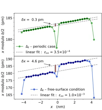
3FIG. 3. Atomic shift ∆`associated with the interplane
dis-tance b/2 in the direction x, i.e. [1 ¯1 0 0]. The atomic config-urations have 128 atoms. Top: two IDB with periodic bound-ary conditions. Bottom: one IDB and two free surfaces. The plots are centered on a IDB and the vertical origins are ar-bitrary. The grain shift δx and the strain εxx are extracted
from the linear interpolations through the data of each do-main (darker disks). One Ga xy-layer is used in the calcu-lation. The deviating values of ∆` in the middle and at the
extremities correspond to the atomic relaxations at the IDB and at the free surfaces.
a shift δz in agreement with the experiment, reinforces our conclusions.
Boundary conditions – Electrostatic effects — To as-sess the role of the boundary conditions on our results, calculations with free boundary conditions have also been carried out with the PBE functional. Instead of the two interacting IDB – due to the artificial periodicity per-pendicular to the interfaces – there are now possible in-teractions between one IDB and the free surfaces par-allel to it (configurations shown in figures S12 and S13 in Supporting Information30). The initial surfaces has been obtained by truncating the lattice perpendicularly to the [1 ¯1 0 0] direction and are therefore non polar24
(see figure S10 in Supporting Information30). No
exter-nal atoms have been added at these (1 ¯1 0 0)-surfaces to passivate them, in order to get the clean-surface effects. All the atoms have been allowed to relax. The calcu-lated relaxations of these bare surfaces are in agreement with those of previous studies20,33–36, with a contraction
and a rotation of the Ga-N bonds at the surface, the Ga atoms being displaced inward (see also table S2 and figure S11 in Supporting Information30). For all configu-rations studied from 32 atoms up to 128 atoms, the IDB has two stable configurations. The domains are shifted
by δz = 8 pm in those with the lowest energy and by -1 pm in the metastable ones. These results are in agree-ment with those obtained above with periodic boundary conditions, and thus with the experimental results.
Because of the IDB interactions and the resulting strain, we have seen above that the ideal domain sep-aration at the IDB, or equivalently the shift δx to the crystalline interplanar distance d1 ¯1 0 0, is more difficult
to precisely determine37 than the shift δz. Moreover,
with free surfaces parallel to the IDB, we don’t have the computer box periodicity to fix the total length of the configuration along x, and we can’t plot energy curves like in Fig. 2. Thus, to carefully measure δx, we in-troduce a phase method where the atomic positions are compared to a reference crystal. This method is analog to the calculation of the hull function describing atomic displacements when two incommensurate structures are interacting18. It is also similar to the geometrical phase
analysis38–40, used in high resolution electron microscopy
to measure displacement and strain fields in materials. In this last method however, inputs are images and the vari-ation from a lattice reference is processed through Fourier space. When data are atomic coordinates given by com-putations, an atomic phase can be simply calculated for each atom ` as Φ` = 2π(r` · q mod 1), where q is a
chosen reciprocal vector of the reference lattice and r` is
the position of atom `. Here, to get the atomic displace-ments in length unit along direction q, we plot ∆`= u`
mod (1/kqk) versus u`= r`· q/kqk. Note that 1/kqk is
the interplanar distance corresponding to q. Thus, the atomic phases and the atomic shifts associated with q are related by Φ`= ∆`2π/kqk.
In our particular case, the value δx as well as the elas-tic strain in the crystal grains can be extracted from the plot associated with kqk = 2/b in the x-direction. This is shown in figure 3 for the periodic system and for the system with free-surfaces. In both cases the crystalline grains are in tension. However, the strain εxx is 3 times
larger in the free-surface case, and thus the mixed in-teractions between surfaces and IDB are larger than the interactions between the IDB themselves. We have not enough results to deduce the variations of εxxversus
dis-tances, but we have indeed checked the logical result that it decreases with the system sizes. With surfaces, we found a larger grain shift δx than with periodic conditions (see also figure S5 in Supporting Information30). Taking into account that these systems are under a larger stress, the periodic boundary conditions give a more reliable re-sult. We can conclude that the domain shift δx is close to zero. This is indeed in agreement with the experimen-tal results of Ref. 2 where it is concluded from the value of their error bar that δx < 4 pm. Note however that the value δx obtained with free surfaces is due to electro-static interactions between the IDB and the free surfaces and thus, could be present in thin nanowires where IDB can be close to the surface8,9.
Conclusion — Several experimental techniques are under development to reach the picometer resolution and
to study extended defects, especially in semiconductors where they play an important role on the physical prop-erties of electronic and optoelectronic devices. These techniques are mostly based on the interference of co-herent x-ray2,41 and electron diffraction42 beams, or on
the scanning of transmitted electron beam by correct-ing both spherical aberrations and distortions7,43. As in the calculation, they require a portion of good crystal to provide a reference in order to estimate the lattice dis-placements induced by the presence of extended defects. In parallel to these experimental works, ab initio cal-culations should now attempt to reach a similar goal to enable cross-talks between experiment and theory. Along this line, we have revisited here the theoretical basis of IDB∗, focusing on the detail of its structure, and this resolution can indeed be reached in gallium nitride. To achieve this accuracy, which is validated by experimental results, we have taken advantage of the high precision achieved by the DFT code22and by a favorable behavior
of simulations for the GaN compound. The high precision of the calculations comes from different characteristics of the program, in particular the type of wavelet basis and their implementation21. The mark of these ingredients is
the regularity of the energy and phase curves (Fig 2 and 3) with sub-picometer input variations (see also figure S5 in Supporting Information30).
For the well-established IDB∗structure, we found that the GaN inversion domains are subjected to a positive or a negative extra lattice shift parallel to the hexagonal axis leading to two states, respectively IDB+ and IDB−.
The positive shift δz leads to the ground state and its value of 8 pm is in agreement with the reported experi-mental results2. We have carefully checked the effects of
the boundary conditions. Like the size of the configura-tions, they do not change the ground state status of the two minima, neither their respective values of δz. Note that in simulations with Tersoff-Brenner potentials for GaN, i.e. without electronic density taken into account, only one minimum had been found2. GaN wurtzite is a strongly polarized compound and we could expect a sim-ilar behavior for IDB in wurtzite ZnO, which has very similar physical properties.
While our various calculations of δz converge, the do-main shift δx, perpendicular to the interface, is more dependent on the boundary conditions. The interactions between surface and IDB are strong for the configuration sizes studied here, and periodic conditions are recom-mended, as usual, for this determination. Nevertheless, for thin wires grown by molecular beam epitaxy where IDB can be located very close to the surface, our results with free-surface conditions can be pertinent and predict larger values of δx than in the bulk. Determined with pe-riodic conditions, the shift δx for the bulk is lower than half a picometer. Experimentally, this value is difficult to measure too, but the interval given2 of δx < 4 pm is
in agreement with our result. Supplemental Material —
6 following information:
(1) k-point grid and h-grid parameter convergences; (2) lattice parameter determinations; (3) grain-shift δx con-vergence; (4) plots of the atomic configuration and the electron density of IDB+; (5) grain-shift δz with LDA;
(6) surface relaxation; (7) collection of ball-and-stick models; (8) Hessian matrix calculation; (9) list and de-scription of the atomic-configuration files that are also available as Supplemental Material.
Appendix: Grain shift δz
The grain shift δz is the main quantity of the system that indicates a discrepancy between the original IDB∗ model14 and our calculation, as well as with the exper-imental results2. It is therefore crucial to calculate it
carefully. This could be done by using the phase method introduced above. Indeed, in the same way as the shift δx has been calculated, we could calculate δz using the c-lattice parameter instead of the b one, i.e. with ∆`= z`
mod c/2. However in an atomic row perpendicular to
the IDB, the coordinate z varies by a much lower quan-tity than c/2. Thus plotting z` versus x is enough to
determine δz.
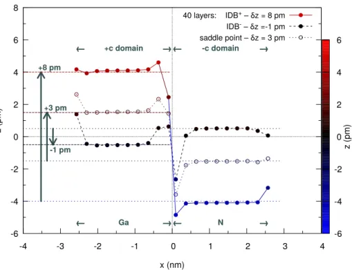
Figure 4 shows the atomic coordinates z`, as well as the
global shifts δz found for three states: the ground-state IDB+, the metastable state IDB−, and the saddle-point
state separating IDB+ and IDB−. This figure and
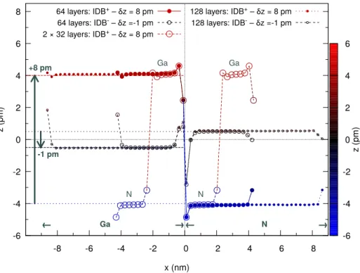
fig-ure 5 show the precision achieved by the calculations and the consistency of the results with the system size. More generally, figures 3 and 4 show the atomic relaxations at the interface respectively along x and z. No relaxation occurs along y.
ACKNOWLEDGMENTS
The authors thank Damien Caliste for his open soft-ware V Sim, which has allowed us to visualize the atomic configurations and the electronic densities. They also thank Thierry Deutsch for useful discussions and sugges-tions. -6 -4 -2 0 2 4 6 8 -4 -3 -2 -1 0 1 2 3 4 → Ga ← ← N → → +c domain ← ← -c domain → +8 pm +3 pm -1 pm z (pm) x (nm) 40 layers: IDB+ – δz = 8 pm IDB- – δz =-1 pm saddle point – δz = 3 pm -6 -4 -2 0 2 4 6 z (pm)
FIG. 4. Atomic coordinate z along the hexagonal axis [0 0 0 1] versus the position x along [1 ¯1 0 0], i.e. perpendicular to the interface. One atomic layer crossing orthogonally the interface is considered for this graph. It consists of Ga atoms on one side (+c domain) and N atoms on the other side (-c domain). The results are for three 80-atom configurations (i.e. with 40 layers parallel to the IDB): the ground state IDB+, the metastable state IDB−, and the saddle-point state. They correspond respectively to domain shifts δz equal to +8.2 pm, -1.0 pm, and +3.1 pm.
-6 -4 -2 0 2 4 6 8 -8 -6 -4 -2 0 2 4 6 8 → Ga ← Ga N Ga N ← N → +8 pm -1 pm z (pm) x (nm) 64 layers: IDB+ – δz = 8 pm 64 layers: IDB- – δz =-1 pm 2 × 32 layers: IDB+ – δz = 8 pm 128 layers: IDB+ – δz = 8 pm 128 layers: IDB- – δz =-1 pm -6 -4 -2 0 2 4 6 z (pm)
FIG. 5. Summary of the results for 128-atom and 256-atom configurations (64 and 128 layers respectively) showing the atomic coordinate z along the hexagonal axis versus the position x perpendicular to the interface. One special configuration contains four instead of two IDB (2×32 layers), and thus four domains. The coherence of the results among different system sizes is thus validated.
∗
1 Kurt Lejaeghere, Gustav Bihlmayer, Torbjoern
Bjo-erkman, Peter Blaha, Stefan Bluegel, Volker Blum, Damien Caliste, Ivano E. Castelli, Stewart J. Clark, An-drea Dal Corso, Stefano de Gironcoli, Thierry Deutsch, John Kay Dewhurst, Igor Di Marco, Claudia Draxl, Marcin Dulak, Olle Eriksson, Jose A. Flores-Livas, Kevin F. Garrity, Luigi Genovese, Paolo Giannozzi, Mat-teo Giantomassi, Stefan Goedecker, Xavier Gonze, Oscar Granaes, E. K. U. Gross, Andris Gulans, Fran¸cois Gygi, D. R. Hamann, Phil J. Hasnip, N. A. W. Holzwarth, Diana Iusan, Dominik B. Jochym, Fran¸cois Jollet, Daniel Jones, Georg Kresse, Klaus Koepernik, Emine Kuecuekbenli, Yaroslav O. Kvashnin, Inka L. M. Locht, Sven Lubeck, Martijn Marsman, Nicola Marzari, Ulrike Nitzsche, Lars Nordstrom, Taisuke Ozaki, Lorenzo Paulatto, Chris J. Pickard, Ward Poelmans, Matt I. J. Probert, Keith Refson, Manuel Richter, Gian-Marco Rignanese, Santanu Saha, Matthias Scheffler, Martin Schlipf, Karlheinz Schwarz, Sangeeta Sharma, Francesca Tavazza, Patrik Thunstroem, Alexandre Tkatchenko, Marc Torrent, David Vanderbilt, Michiel J. van Setten, Veronique Van Speybroeck, John M. Wills, Jonathan R. Yates, Guo-Xu Zhang, and Stefaan Cottenier, “Reproducibility in density functional theory calculations of solids,” Science 351, 1415–U81 (2016).
2
St´ephane Labat, Marie-Ingrid Richard, Maxime Dupraz,
Marc Gailhanou, Guillaume Beutier, Marc Verdier, Francesca Mastropietro, Thomas W. Cornelius, Tobias U. Sch¨ulli, Jo¨el Eymery, and Olivier Thomas, “Inversion domain boundaries in GaN wires revealed by coher-ent bragg imaging,” ACS Nano 9, 9210–9216 (2015), http://dx.doi.org/10.1021/acsnano.5b03857.
3
L. T. Romano, J. E. Northrup, and M. A. O’Keefe, “Inver-sion domains in GaN grown on sapphire,” Applied Physics Letters 69, 2394–2396 (1996).
4
J.L. Rouvi`ere, M. Arlery, B. Daudin, G. Feuillet, and O. Briot, “Transmission electron microscopy structural characterisation of GaN layers grown on (0001) sapphire,” Materials Science and Engineering: B 50, 61 – 71 (1997).
5
Jean-Luc Rouvi`ere, M. Arlery, and Alain Bourret, “Struc-tural characterisation of GaN layers : influence of polarity and strain release,” Institute of Physics Conference Series 157, 173–182 (1997), presented at the Royal Microscopi-cal Society Conference on Microscopy of Semiconducting Materials, 7-10 April 1997. Article reprint from Jean-Luc.
6
A. M. Sanchez, G. Nouet, P. Ruterana, F. J. Pacheco, S. I. Molina, and R. Garcia, “A mechanism for the multiple atomic configurations of inversion domain boundaries in GaN layers grown on Si(111),” Applied Physics Letters 79, 3588–3590 (2001).
7 Fude Liu, Ramon Collazo, Seiji Mita, Zlatko Sitar,
ob-8
servation of inversion domain boundaries of GaN on c-sapphire at sub-˚Angstrom resolution,” Advanced Materials 20, 2162–2165 (2008).
8
X. J. Chen, G. Perillat-Merceroz, D. Sam-Giao, C. Durand, and J. Eymery, “Homoepitaxial growth of catalyst-free GaN wires on N-polar substrates,” Applied Physics Letters 97, 151909 (2010), https://doi.org/10.1063/1.3497078.
9
Thomas Auzelle, Benedikt Haas, Martien Den Hertog, Jean-Luc Rouvi`ere, Bruno Daudin, and Bruno Gayral, “Attribution of the 3.45 eV GaN nanowires luminescence to inversion domain boundaries,” Applied Physics Letters 107, 051904 (2015).
10
Aref Chowdhury, Hock M. Ng, Manish Bhardwaj, and Nils G. Weimann, “Second-harmonic generation in period-ically poled GaN,” Applied Physics Letters 83, 1077–1079 (2003), http://dx.doi.org/10.1063/1.1599044.
11
Jennifer Hite, Mark Twigg, Michael Mastro, Jaime Fre-itas, Jerry Meyer, Igor Vurgaftman, Shawn O’Connor, Nicholas Condon, Fritz Kub, Steven Bowman, and Charles Eddy, “Development of periodically oriented gallium ni-tride for non-linear optics,” Opt. Mater. Express 2, 1203– 1208 (2012).
12
Jennifer K. Hite, Nelson Y. Garces, Ramasis Goswami, Michael A. Mastro, Fritz J. Kub, and Charles R. Eddy Jr., “Selective switching of GaN polarity on Ga-polar GaN using atomic layer deposited Al2O3,” Applied Physics
Ex-press 7, 025502 (2014).
13 J.L. Rouvi`ere, M. Arlery, R. Niebuhr, K.H. Bachem, and
O. Briot, “Transmission electron microscopy characteriza-tion of GaN layers grown by MOCVD on sapphire,” Ma-terials Science and Engineering: B 43, 161 – 166 (1997), e-MRS 1996 Spring Meeting, Symposium C: UV, Blue and Green Light Emission from Semi-conductor Materials.
14
John E. Northrup, J¨org Neugebauer, and L. T. Romano, “Inversion domain and stacking mismatch boundaries in GaN,” Phys. Rev. Lett. 77, 103–106 (1996).
15
P. J. Schuck, M. D. Mason, R. D. Grober, O. Ambacher, A. P. Lima, C. Miskys, R. Dimitrov, and M. Stutz-mann, “Spatially resolved photoluminescence of inver-sion domain boundaries in GaN-based lateral polarity heterostructures,” Applied Physics Letters 79, 952–954 (2001).
16
Ronny Kirste, Ram´on Collazo, Gordon Callsen, Markus R. Wagner, Thomas Kure, Juan Sebastian Reparaz, Seji Mita, Jinqiao Xie, Anthony Rice, James Tweedie, Zlatko Sitar, and Axel Hoffmann, “Temperature dependent photolu-minescence of lateral polarity junctions of metal organic chemical vapor deposition grown GaN,” Journal of Applied Physics 110, 093503 (2011).
17
Vincenzo Fiorentini, “Origin of the efficient light emis-sion from inveremis-sion domain boundaries in GaN,” Applied Physics Letters 82, 1182–1184 (2003).
18
A. Gautam, C. Ophus, F. Lan¸con, V. Radmilovic, and U. Dahmen, “Atomic structure characterization of an in-commensurate grain boundary,” Acta Materialia 61, 5078 – 5086 (2013).
19 M. Leszczynski, H. Teisseyre, T. Suski, I. Grzegory,
M. Bockowski, J. Jun, S. Porowski, K. Pakula, J. M. Bara-nowski, C. T. Foxon, and T. S. Cheng, “Lattice parame-ters of gallium nitride,” Applied Physics Letparame-ters 69, 73–75 (1996).
20
Jes´us Z´u˜niga P´erez, Vincent Consonni, Liverios Lymper-akis, Xiang Kong, Achim Trampert, Sergio Fern´ andez-Garrido, Oliver Brandt, Hubert Renevier, Stacia Keller,
Karine Hestroffer, Markus R. Wagner, Juan Sebasti´an Reparaz, Fatih Akyol, Siddharth Rajan, St´ephanie Ren-nesson, Tom´as Palacios, and Guy Feuillet, “Polarity in gan and zno: Theory, measurement, growth, and devices,” Applied Physics Reviews 3, 041303 (2016), https://doi.org/10.1063/1.4963919.
21
Luigi Genovese, Alexey Neelov, Stefan Goedecker, Thierry Deutsch, Seyed Alireza Ghasemi, Alexander Willand, Damien Caliste, Oded Zilberberg, Mark Rayson, Anders Bergman, and Reinhold Schneider, “Daubechies wavelets as a basis set for density functional pseudopotential cal-culations,” The Journal of Chemical Physics 129, 014109 (2008).
22
BigDFT, “version 1.8,” (2016).
23 Alessandro Cerioni, Luigi Genovese, Alessandro Mirone,
and Vicente Armando Sole, “Efficient and accurate solver of the three-dimensional screened and unscreened poisson’s equation with generic boundary conditions,” The Journal of Chemical Physics 137, 134108 (2012).
24
V.M. Bermudez, “The fundamental surface science of wurtzite gallium nitride,” Surface Science Reports 72, 147 – 315 (2017).
25
S. Goedecker, M. Teter, and J. Hutter, “Separable dual-space gaussian pseudopotentials,” Phys. Rev. B 54, 1703– 1710 (1996).
26
C. Hartwigsen, S. Goedecker, and J. Hutter, “Relativistic separable dual-space Gaussian pseudopotentials from H to Rn,” Phys. Rev. B 58, 3641–3662 (1998).
27
John P. Perdew, Kieron Burke, and Matthias Ernzerhof, “Generalized gradient approximation made simple,” Phys. Rev. Lett. 77, 3865–3868 (1996).
28 Philipp Haas, Fabien Tran, and Peter Blaha, “Calculation
of the lattice constant of solids with semilocal functionals,” Phys. Rev. B 79, 085104 (2009).
29 Luigi Genovese and Thierry Deutsch,
“Multipole-preserving quadratures for the discretization of functions in real-space electronic structure calculations,” Phys. Chem. Chem. Phys. 17, 31582–31591 (2015).
30
See Supplemental Material at [URL will be inserted by publisher] for the supporting pdf document.
31 Frank Eckert, Peter Pulay, and Hans-Joachim Werner,
“Ab initio geometry optimization for large molecules,” Journal of Computational Chemistry 18, 1473–1483 (1997).
32 Eduardo Machado-Charry, Laurent Karim B´eland,
Damien Caliste, Luigi Genovese, Thierry Deutsch, Nor-mand Mousseau, and Pascal Pochet, “Optimized energy landscape exploration using the ab initio based activation-relaxation technique,” The Journal of Chemical Physics 135, 034102 (2011).
33 John E. Northrup and J. Neugebauer, “Theory of
GaN(1010) and (1120) surfaces,” Phys. Rev. B 53, R10477–R10480 (1996).
34 Alessio Filippetti, Vincenzo Fiorentini, Giancarlo
Cap-pellini, and Andrea Bosin, “Anomalous relaxations and chemical trends at iii-v semiconductor nitride nonpolar surfaces,” Phys. Rev. B 59, 8026–8031 (1999).
35 M.-H Tsai, O.F Sankey, K.E Schmidt, and I.S.T Tsong,
“Electronic structures of polar and nonpolar GaN sur-faces,” Materials Science and Engineering: B 88, 40 – 46 (2002).
36
David Segev and Chris G. Van de Walle, “Surface recon-structions on InN and GaN polar and nonpolar surfaces,” Surface Science 601, L15 – L18 (2007).
37
Stefan Goedecker, Fr´ed´eric Lan¸con, and Thierry Deutsch, “Linear scaling relaxation of the atomic positions in nanos-tructures,” Phys. Rev. B 64, 161102 (2001).
38
Mitsuo Takeda and Jun Suzuki, “Crystallographic hetero-dyne phase detection for highly sensitive lattice-distortion measurements,” J. Opt. Soc. Am. A 13, 1495–1500 (1996).
39
M.J. H¨ytch, E. Snoeck, and R. Kilaas, “Quantitative mea-surement of displacement and strain fields from hrem mi-crographs,” Ultramicroscopy 74, 131 – 146 (1998).
40
J.L. Rouvi`ere and E. Sarigiannidou, “Theoretical discus-sions on the geometrical phase analysis,” Ultramicroscopy 106, 1 – 17 (2005).
41
S.J. Leake, V. Favre-Nicolin, E. Zatterin, M-I. Richard, S. Fernandez, G. Chahine, T. Zhou, P. Boesecke, H. Dja-zouli, and T.U. Sch¨ulli, “Coherent nanoscale X-ray probe for crystal interrogation at ID01, ESRF – the European Synchrotron,” Materials & Design 119, 470–471 (2017).
42 Lijun Wu, Yimei Zhu, and J. Tafto, “Picometer accuracy
in measuring lattice displacements across planar faults by interferometry in coherent electron diffraction,” Phys. Rev. Lett. 85, 5126–5129 (2000).
43
Shoucong Ning, Takeshi Fujita, Anmin Nie, Ziqian Wang, Xiandong Xu, Jianghua Chen, Mingwei Chen, Shuhuai Yao, and Tong-Yi Zhang, “Scanning distortion correction in STEM images,” Ultramicroscopy 184, 274–283 (2018).