A bio-inspired active radio-frequency silicon cochlea
The MIT Faculty has made this article openly available.
Please share
how this access benefits you. Your story matters.
Citation
Mandal, S., S.M. Zhak, and R. Sarpeshkar. “A Bio-Inspired Active
Radio-Frequency Silicon Cochlea.” Solid-State Circuits, IEEE
Journal of 44.6 (2009): 1814-1828. © 2009 IEEE.
As Published
http://dx.doi.org/10.1109/JSSC.2009.2020465
Publisher
Institute of Electrical and Electronics Engineers
Version
Final published version
Citable link
http://hdl.handle.net/1721.1/59982
Terms of Use
Article is made available in accordance with the publisher's
policy and may be subject to US copyright law. Please refer to the
publisher's site for terms of use.
A Bio-Inspired Active Radio-Frequency
Silicon Cochlea
Soumyajit Mandal, Student Member, IEEE, Serhii M. Zhak, and Rahul Sarpeshkar, Senior Member, IEEE
Abstract—Fast wideband spectrum analysis is expensive in
power and hardware resources. We show that the spectrum-anal-ysis architecture used by the biological cochlea is extremely efficient: analysis time, power and hardware usage all scale linearly with , the number of output frequency bins, versus log( ) for the Fast Fourier Transform. We also demonstrate two on-chip radio frequency (RF) spectrum analyzers inspired by the cochlea. They use exponentially-tapered transmission lines or filter cascades to model cochlear operation: Inductors map to fluid mass, capacitors to membrane stiffness and active elements (transistors) to active outer hair cell feedback mechanisms. Our RF cochlea chips, implemented in a 0.13 m CMOS process, are 3 mm 1.5 mm in size, have 50 exponentially-spaced output chan-nels, have 70 dB of dynamic range, consume 300 mW of power and analyze the radio spectrum from 600 MHz to 8 GHz. Our work, which delivers insight into the efficiency of analog computa-tion in the ear, may be useful in the front ends of ultra-wideband radio systems for fast, power-efficient spectral decomposition and analysis. Our novel rational cochlear transfer functions with zeros also enable improved audio silicon cochlea designs with sharper rolloff slopes and lower group delay than prior all-pole versions.
Index Terms—Bio-inspired, cochlear models, radio frequency
(RF), silicon cochlea, spectrum analysis.
I. INTRODUCTION
T
HE mammalian cochlea, or inner ear, is an amazing sen-sory instrument that transforms sound frequencies into spatially and temporally-varying excitation patterns of the au-ditory nerve. It performs this task over a wide range of input frequencies and amplitudes using very little power. In humans, the approximate values of these performance metrics are three decades, 120 dB, and 14 W, respectively [1]. The cochlea is a hydro-mechanical system; incoming sounds set up traveling waves on the basilar membrane (BM) and in the fluids that sur-round it [2], [3]. The properties of the BM scale approximately exponentially with position: The membrane gradually becomes wider and less stiff, and resonates at lower frequencies. Thus, high frequency sounds excite responses towards the beginning, or basal part, of the cochlea, while low frequency sounds excite responses towards the end, or apical part. In other words, the cochlea uses a frequency-to-space transformation to perform audio spectral analysis.Manuscript received November 04, 2008; revised March 17, 2009. Current version published May 28, 2009. The work of S. Mandal was partially supported by a Poitras pre-doctoral fellowship.
The authors are with the Department of Electrical Engineering and Computer Science, Massachusetts Institute of Technology, Cambridge, MA 02139 USA (e-mail: [email protected]).
Digital Object Identifier 10.1109/JSSC.2009.2020465
Active feedback, mediated by outer hair cells (OHCs) lo-cated on the BM, amplifies the amplitude of the cochlear trav-eling wave and improves frequency selectivity. OHCs have been the subject of much research [4]–[12]. The cochlea performs highly resource-efficient distributed computation by exploiting the properties of a physical medium. Distributed analog compu-tation has been used to build several efficient engineering sys-tems, both at radio frequencies (RF) [13]–[16] and at lower fre-quencies [17].
Electronic circuit models of cochlear mechanics, also known as silicon cochleas, have thus far only been integrated on-chip at audio [1], [18]–[21], though simulations of a frequency-shifted cochlear model operating between 300 kHz and 1 MHz were presented in [22]. The idea of an “RF cochlea” was first pro-posed in [23]. A few building-block circuits for this RF cochlea were described in [24]. Some completely passive electronic cochleas that operate at RF using discrete components or multi-chip modules have also recently been reported [25]–[27]. In this paper we demonstrate the first integrated-circuit im-plementation of the cochlear spectrum analysis algorithm using active electronic circuits operating at typical radio frequencies. We use a mechanical-to-electrical mapping to transform pres-sure into voltage , and volume velocity into current , re-spectively. Membrane stiffness is replaced by capacitance, fluid mass by inductance and active feedback mechanisms by circuits that create negative resistances. In this way, we mimic the me-chanics of the biological cochlea, but at frequencies that are six orders of magnitude higher. A key advantage of operating at RF (as opposed to audio) is the availability of passive inductors, which have significantly lower noise and higher dynamic range than active inductors operating with the same power consump-tion [24].
This paper is organized as follows. Section II describes the spectrum analysis algorithm used by the biological cochlea, and analyzes reasons for its efficiency. Section III discusses novel bidirectional and unidirectional cochlear models that efficiently represent properties of the biological traveling wave architecture. Our unidirectional model is also useful for audio silicon cochlea designs. Section IV discusses circuit design of the RF cochlea. Section V discusses experimental results, while Section VI concludes the paper.
II. COCHLEARSPECTRUMANALYSIS
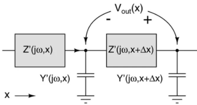
Fig. 1 graphically illustrates three common types of spectrum analyzers, including the cochlea. To first order, the cochlea can be modeled as a transmission line, shown in Fig. 2 where shunt admittances model sections of the BM, while the series im-pedances are inductors modeling fluid coupling. The values of and per unit length increase exponentially with position
Fig. 1. Comparison of the spectral analysis algorithms of (a) the FFT, (b) a parallel bank of independent filters and (c) the cochlea. Blocks represent two-input multiply-and-add units in the FFT, elementary filters in the filter bank and cochlear stages in the cochlea. The ‘triangular’ sliding windows in the cochlea illustrate that cochlear transfer functions are created by contributions from approximatelyN filters basal to that output. Therefore, only one new stage needs to be added to create each new output.
Fig. 2. A generic spatially-varying one-dimensional transmission line, with se-ries impedances represented byZ and shunt admittances by Y .
[23], [28], i.e., , where is a constant that charac-terizes the length scale on which cochlear properties vary from the basal to the apical end [28]. The transfer function of the cochlea is defined as the normalized current that flows through in response to a input tone with frequency [28]. It models the velocity of the BM. At a given position, the magnitude of the TF slowly increases with frequency, reaches its
maximum value near a frequency ,
known as the center frequency, and then rapidly decreases. In order to model the continuous cochlear transmission line with a finite number of components we spatially discretize it by lumping sections of line long into individual stages. We assume is constant; as a result the stages have
exponentially-spaced center frequencies. The number of stages per e-fold in center frequency is given by
(1) The exponentially-tapered structure of the cochlea ensures that the TF at any position is produced by a “sliding window” of the approximately stages basal of that position, as shown in Fig. 1. The magnitude of each TF peaks around its center frequency , and thus selects a frequency “bin” centered about
. Any cochlear TF is well approximated as a cascade of identical stages, which gives cochlear TFs a very sharp rolloff slope [1]. The frequency resolution of the cochlea is ultimately set by the sharpness of these high-frequency roll-off slopes, which for a given signal-to-noise ratio, sets the minimum frequency ratio that can be discriminated by adjacent cochlear stages.
The analysis time of a spectrum analyzer is defined as the time taken to resolve the -th frequency bin. In the cochlea, the analysis time is equal to the sum of the settling times of stages basal of , which is approximately equal to . There-fore, the analysis time for the whole spectrum is on the order of cycles of the lowest analyzed frequency. In addition, the total number of stages is given by , where is the ratio of maximum and minimum analyzed fre-quencies, and the ‘1’ accounts for the fact that the very first cochlear output needs an extra stages basal to it. Thus, for a
given value of , we get , which implies that . In order to make the shape of TF independent of we implement cochlear stages as frequency-scaled versions of a common pro-totype [18]. As a result, the hardware and power requirements of the cochlea also scale as the total number of filters, i.e., .
A parallel bank of constant- , independent filters can also be used to decompose a signal into exponentially-spaced fre-quency bins. In order to get frefre-quency resolution similar to the cochlea each independent filter must have order . Such fil-ters can be formed by cascading second-order filter stages, as shown in Fig. 1. There are such filters, which, unlike in the cochlea, are not shared between outputs. Thus, the hard-ware cost, as measured by the total number of second-order filter stages, scales like if is fixed. However, the time taken for spectrum analysis in the filter bank is given by the sum of the settling times of the sections in each filter, which scales like .
The output bins of both the cochlea and parallel filter banks are available and updated in parallel, which allows them to tinuously monitor the whole spectrum. This behavior is in con-trast to most commercial RF spectrum analyzers, which are of the swept-sine or super-heterodyne type. In this type of ana-lyzer a single frequency bin is sampled and updated at a given time, causing aliasing of non-stationary spectra. The sampling rate scales as , i.e., the time to analyze the whole spectrum scales as [29]. However, the hardware requirements for this type of analyzer are independent of , i.e., .
The Fast Fourier Transform (FFT) uses constant-bandwidth frequency bins, unlike the cochlea and constant- parallel filter banks. It takes time (measured by the number of multiply-and-add operations) and uses hardware (measured by the number of multipliers and adders) to perform spectrum analysis.
Thus, it appears that the cochlear spectral analysis algorithm delivers the most efficient trade-off between analysis time and hardware cost. It exploits the scale-invariant nature of an expo-nential to achieve scaling in both quantities.
III. SYSTEMDESIGN
A. Bidirectional Cochlear Model
The equations for voltage (corresponding to fluid pressure ) and current (corresponding to volume velocity ) on the spatially-varying transmission line shown in Fig. 2 in sinusoidal steady-state are given by
(2) where and are the impedance and admittance
per unit length of the line. We now define as a dimensionless frequency variable that is normalized by the
center frequency at the position of
interest. Because of the exponential scaling in the cochlea, we
have and
, i.e., the impedances and admittances at any two posi-tions in the cochlea are identical if we exponentially scale the frequencies at which they are compared.
Since , we can eliminate the separate depen-dencies on and by rewriting (2) as
(3) Hereafter, we use the convention that and refer to impedance and admittance per unit length in the continuous transmission line, and refer to impedances and admit-tances in the spatially-discretized, or lumped transmission line, and and are normalized, dimensionless forms of and . Each stage contains a series impedance and a shunt admittance , given by
(4) The series impedance consists of an inductance that models fluid mass and increases exponentially with position, resulting in
(5)
where , and is the inductance per unit
length at . The normalized, dimensionless forms of and are given by
(6) The normalizing impedance is a constant that, in a real implementation, scales all dimensionless impedances and pro-vides a degree of freedom in the design. In the RF cochlea, is chosen to make on-chip implementation practical, as we dis-cuss later. From (5) and (6), is given by
(7)
where is a dimensionless constant. The
normalized shunt admittance models the complex behavior of the organ of Corti. In an important paper [28], Zweig used experimental measurements to propose the following form for
:
(8) where and are constants. Zweig’s admittance function can be interpreted as a feedback loop containing an RLC res-onator and a pure delay. Its frequency response is shown in Fig. 3 for the following parameter values (obtained from [28]): . Unfortunately, the function cannot be synthesized with a finite number of lumped circuit elements because it is not rational. We therefore used
Fig. 3. Normalized BM admittanceY proposed by Zweig [28].
a rational function to approximate (8), [30]. The function we chose is given by
(9) where and are constants. This admittance is the simplest rational function that contains all essential features of (8). These features are: two pairs of high-Q complex poles, a pair of zeros, capacitive behavior at low frequencies, and inductive behavior at high frequencies. Allowable values of and at all am-plitudes are constrained by the requirement that zero-crossings in the transient response remain approximately invariant with input amplitude, like in the biological cochlea [10]. We used the following parameter values in our bidirectional cochlea
de-sign: and . The resultant form of ,
which is shown in Fig. 4(a) and (b), is quite similar to Zweig’s function, which is shown in Fig. 3.
At frequencies much smaller than the maximum operating frequency the input impedance of the cochlea is given by the following standard expression for a continuous transmission line with series impedances and shunt admittances :
(10) When , we see from (9) that . Therefore, at frequencies that are much smaller than the local center fre-quency looks like a capacitor. Substituting for and in (10), we find that the input impedance at frequencies much smaller than is given by
(11) We usually fix for compatibility with standard RF test equipment. The sizes of capacitors in the design scale like
(12)
Fig. 4. (a) Normalized BM admittanceY used in the cochlea. (b) Pole-zero plot forY .
Equivalently, we have . The exponential de-crease of center frequency with position is accomplished by increasing inductor and capacitor values in and expo-nentially with stage number , i.e., making and (and all other inductors and capacitors used to implement ) scale as
, while resistances remain fixed [31], [32]. The system of first-order ODEs shown in (3) can be combined into a single second-order ODE, given by
(13)
where is a dimensionless
variable. If was constant with , as in an uniform trans-mission line, the solution to (13) would simply be the complex exponential . Now assume that is not constant, but, as in the cochlea, varies slowly with , i.e., such that . In this case, we can use the well known
Wentzel-Kramers-Brillouin (WKB) approximation to solve (13), [28]. The result is
(14) where is a constant. The transfer function (TF) of the cochlea, which is defined as the current flowing through the shunt ad-mittance , normalized by the input current [28], can be written as
(15) Substituting from (3) in (15), and remembering that
, we find that
(16) We can substitute from (14) into the expression for the cochlear TF defined in (16), to find that the cochlear TF is proportional to
(17) where and are constants determined by and boundary conditions. The two terms correspond to wave prop-agation in the (forward) and (reflected) directions. The reflected wave is undesirable, and its amplitude should be min-imized.
The center frequency of the last, or apical, cochlear stage
is given by , where is
the total number of stages. In order to reduce reflections from the apex the transmission line must be terminated with an impedance-matched load. We found that a termination impedance consisting of a resistor in series with an inductor provides adequate matching over the frequency range of
interest, namely . We use , which
provides a match at frequencies much smaller than . We also make the magnitude of ’s impedance at equal to . which provides a match at frequencies comparable to
. Thus, is given by
(18) In order for our lumped transmission line to closely approxi-mate the original continuous line each stage should only change the phase of TF, i.e., , by a small amount. If this con-dition is not met the spatial discretization becomes too coarse, resulting in unwanted inter-stage reflections that show up as
sec-ondary peaks in the cochlear TF. In order to avoid such reflec-tions, we should have
(19) where is the change in due to a single stage, and we have used the fact that . Thus, inter-stage reflections increase as , the ratio of the input frequency to the best frequency at that location, increases. In other words, a fixed-frequency input tone will suffer increasing reflections as it propagates, since decreases exponentially with in-creasing .
For a given value of , inter-stage reflections can be reduced by reducing and increasing . However, signal gain, i.e., , increases with , as may be seen from (17). On the other hand increasing is undesirable because of increased chip area, power consumption, and output noise. The designer must compromise between these conflicting performance re-quirements.
By substituting and using the known
values of and , the no-reflection condition in (19) can be rewritten as
(20) Since the values of and are fixed, we must reduce to reduce inter-stage reflections. The quantity has a simple physical interpretation: it is the ratio of the amount of reactive energy stored within each stage, which is given by , to the energy transferred per cycle (i.e., in a time ) to the other stages. The latter quantity is given by , where is the current along the line. Using (12), we can also rewrite in the suggestive form
(21)
Here is the cutoff frequency of the
lumped transmission line. Wave propagation on lumped lines is only possible at frequencies less than the cutoff frequency.
B. Unidirectional Cochlear Model
In the biological cochlea, backward wave propagation is rel-atively unimportant except for the production of otoacoustic emissions [11]. If we ignore such waves, the bidirectional trans-mission line can be simplified into a cascade of unidirectional filters. We refer to this architecture as the unidirectional RF
cochlea.
The transfer functions for filters in the unidirectional cochlea can be derived from a WKB-type solution of the wave equation by making a series of further approximations [24], [30]. The essence of cochlear operation is collective amplifica-tion, as exemplified by the exponential part of the transfer func-tion shown in (17). For simplicity, therefore, we ignore the
pre-exponential terms. The reflected wave is also neglected, making the structure unidirectional. The exponential term is modeled by breaking up the integral, which extends from 0 to , into small parts extending from to , where is an integer:
(22) We note that the expression above looks like the transfer func-tion of a cascade of unidirecfunc-tional filters with transfer funcfunc-tions . We assume that each filter models the action of a piece of transmission line long. Thus, the th filter models the piece
of line between and . By using the
definition of , we have
(23) where . Thus, the values of increase expo-nentially, i.e., proportional to . In other words, we have filters per e-fold in frequency. Now define
. If is large enough, we may assume that re-mains approximately constant between and . Therefore, the integral that defines can be simplified to
(24)
If and each transfer function can
be approximated by using the identity since . Also, we may write
. Therefore, is given by
(25)
We see that each transfer function is only a function of , which scales exponentially along the cascade, and , which is constant, but can differ from its value in the bidirectional cochlea. Therefore, the transfer functions are simply frequency-scaled versions of each other and we can represent all of them using the single normalized frequency variable . By substi-tuting in , we get the following normal-ized transfer function:
(26) In order to make rational, we choose in (9). This choice makes a perfect square, and is given by
(27) where , as in the bidirectional cochlea. We used the following parameter values in our unidirectional
cochlea design: and [24].
Our filter TF is shown in Fig. 5(a) and (b). Since it contains a pair of poles and a pair of complex zeros, it differs from the
Fig. 5. (a) Normalized TFH used in the unidirectional cochlea. (b) Pole-zero plot forH .
all-pole TF’s previously used to build audio-frequency silicon cochleas [1], [18]. In addition to reducing group delay, the figure shows that the zeros also result in an asymmetric frequency re-sponse close to the peak of the TF, with a sharper drop-off on the high-frequency side that increases the frequency resolution of the cochlear TFs. The filter transfer function actually imple-mented on-chip included an additional high-frequency zero and two additional high-frequency poles because they made the cir-cuit significantly easier to design. These additional poles and zeros do not have a significant effect on the cochlear transfer function.
IV. CIRCUITDESIGN
A. Bidirectional Cochlea
Equation (9) shows that the BM admittance must tend to zero as . However, integrated circuits contain para-sitic capacitances that, at high frequencies, become large admit-tances in parallel with . A more robust design is obtained by reversing the mapping between mechanical and electrical do-mains, i.e., representing pressure by current , and volume
Fig. 6. The impedance-transformed cochlear model that was implemented on-chip.
velocity by voltage . This new mapping transforms imped-ances to admittimped-ances and vice versa, so we get the transmis-sion line structure shown in Fig. 6, where and . The output variable changes from the shunt current to the voltage across the series impedances, i.e., . Note that parasitic shunt capac-itances can now be absorbed into the line. Another advantage of this design is that the output, being the difference in voltage be-tween two nodes, is resistant to unwanted common-mode sig-nals on the ground node. The wave number is unchanged and the cochlear TFs have the same frequency dependence as be-fore. However, impedances and admittances are interchanged, so the series termination network becomes a parallel network. We used the following parameter values in our bidirectional cochlea implementation:
rad/s, fF,
and .
For the realistic parameter values used to draw Fig. 4(a), the series impedance is not physically realizable using only pas-sive elements. In fact, it needs at least two resistances, one of which, say , must be negative to pump energy into the trav-eling wave in regions basal of the peak and increase gain. The second resistance must be positive for overall stability. A simplified version of our stage design is shown in Fig. 7. Each consists of two resonators that are coupled both inductively and capacitively.
At positions far before the peak the negative resistance cannot pump energy into the traveling wave, since is domi-nated by the inductor . Any parasitic series resistance in now absorbs energy from the wave, causing it to attenuate. An additional negative resistance, in parallel with the shunt admittance is used to cancel such attenuation.
A more complete circuit diagram of our implementation of a single bidirectional cochlea stage is shown in Fig. 8. The DC voltage on the line (i.e., the DC value of and for every stage) is determined by a low-frequency negative feedback loop that sets to an appropriate value. The loop, which runs con-tinuously, uses an integrator to sense the DC line voltage and sets it equal to a reference voltage, normally . It does not interfere with normal cochlear operation because it has very low bandwidth.
A cross-coupled pair of nMOS transistors, and , cre-ates the negative resistance . The bias current through
the pair is set by the control voltage . The impedance pro-duced by the cross-coupled pair between and consists of a resistance in parallel with a capacitance , where , the small signal transconduc-tance, is an increasing function of , and and are the gate-source and gate-drain capacitances, respectively. An im-portant advantage of this topology is that can be absorbed into .
The low-frequency line loss cancellation network is a single-ended negative resistor that is created in two stages. The voltage at is first amplified by a common-source amplifier. The output of this amplifier controls a current source, , that can sink or source current from . Because of the sign inver-sion produced by the amplifier, pushes current into the node when the voltage on it rises (and vice-versa) thereby creating a negative resistance of value , where is the transconductance of and (assumed equal). The value of , and thus , is set by the bias voltage . The value of is made large enough for the pole frequency to be much smaller than the center frequency at the location of in-terest, allowing the amplifier to reject the DC value of and only respond to RF (i.e., have a highpass characteristic). Without this loss-cancellation network, low frequencies would be
atten-uated by a factor at every stage,
where is the parasitic series resistance of (not drawn).
With by design and a typical , signals
that peak at the end of the cochlea (after 50 stages) would be attenuated by a factor of about ( 40 dB) before reaching the apex.
The output voltages are pre-amplified before their envelopes are detected and read out. Each pre-amplifier is a two stage, resistively-loaded, common source differential am-plifier, with shunt-peaking in the early stages to increase the bandwidth and a voltage gain of approximately
dB. Each envelope detector (ED) uses a diode-connected tran-sistor for rectification and has a dead zone, for small signals, that is approximately equal to , the linear range of the transistor. Here is the thermal voltage and is the sub-threshold constant. The preamplifiers reduce the input-referred dead-zone by a factor of , resulting in a detection threshold
of mV .
B. Unidirectional Cochlea
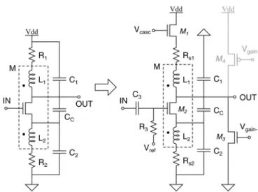
A simplified circuit diagram of our implementation of a single unidirectional cochlea filter is shown on the left-hand side of Fig. 9. Each filter, like in the bidirectional version, consists of two resonators that are coupled both inductively and capaci-tively. The transistor provides active gain and buffering. This topology is efficient because it uses a single transistor while also allowing parasitic capacitances associated with and to be absorbed into and .
A more detailed schematic of the filter is shown on the right-hand side of Fig. 9. The first important change from the simpli-fied circuit shown on the left is that the resistor has been real-ized with an active element. The resistance seen looking into the source of the cascode transistor is given by , where
Fig. 7. Simplified bidirectional cochlea circuit diagram.
Fig. 8. A more detailed circuit diagram of a single bidirectional cochlea stage.
is the small-signal transconductance of . To this resis-tance we must add , the parasitic series resistance of ,
i.e., we have . By implementing with
a transistor we isolate from the power supply, eliminating the effect of parasitic inductances present there. The high-pass filter formed by and is designed to decouple the DC op-erating points of individual stages but act as a short at RF. At “low” frequencies (lower than the center frequency of the stage, but higher than the cut-in frequency of and ), the voltage gain of the filter is given by
(28)
Fig. 9. A circuit diagram of a single unidirectional cochlea filter: simplified version on the left, more detailed implementation on the right The transistor M was not actually implemented on the current chip (see the text for an expla-nation).
Here is the transconductance of and
is the parasitic series resistance of . In order to prevent low-frequency signals from either attenuating or blowing up as they propagate down the cascade we need to be as close to 1 as possible. Assume for now that carries no bias current. In that case , because and share the same bias current and were designed to have the same geometry. Also, and are parasitic components that are
much smaller than and , so and
. As a result, ,
as required.
However, the equation above is only approximate. Since the inductor is in series with a large resistance, i.e., , it does not need to have a high quality factor. Therefore, we designed to have higher series resistance than in order to save layout area, i.e., . Therefore,
, and we get a value of that is somewhat .
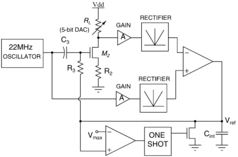
Fig. 10. Feedback loop used to set the bias voltageV .
The voltage sets the current through the transistor . By increasing , we can make carry more current than
, thus making and lowering . In
order to set this low-frequency gain exactly equal to 1 we used a feedback loop. An on-chip oscillator running at 22 MHz con-tinually injects a small calibration tone into the cascade. This signal does not interfere significantly with normal cochlear op-eration since its frequency is much lower than the lowest anal-ysis frequency (600 MHz). The feedback loop uses an integrator to adjust the voltage until the amplitudes of the calibra-tion signal at the beginning and end of the cascade are equal to each other, thus ensuring that the overall low frequency gain is exactly 1.
Experimentally, we found that the gain of the filters was even with . However, the loop as designed could only decrease the gain further by increasing and the current through . The most likely reason for the lowered gain is poorly-modeled parasitic resistances and inductances on the ground node, which increase the effective value of . A simple improvement, to be made in future iterations, is to modify the feedback loop so that it can both add and subtract current from . A simple way to do this is by adding the pMOS transistor (see Fig. 9). We can now increase the gain by low-ering , which increases the DC current through , thus causing to increase without affecting .
The bias voltage sets the value of and . The amount of peaking, or quality factor of each stage is approx-imately , so we can control the sharpness of the cochlear transfer functions by changing via , which is set by the feedback loop shown in Fig. 10. Consider the ampli-fier formed by , which is a replica of the transistor within the filter stages, and . The loop measures input and output amplitudes and adjusts until this amplifier has a gain of 1 at the oscillator frequency (22 MHz). This gain is approximately
, where and is
de-signed to be equal to . Thus, the loop sets , and by adjusting with a resistive DAC, we can control the
peak gain, frequency resolution and power consumption of the cochlea. The switch and monostable (one-shot) resets if it exceeds a reference value , thus ensuring that the loop does not get stuck at the wrong operating point. This precaution is necessary because the relationship between and gain is not monotonic: for very high values of , the gain drops because the transistor comes out of saturation.
The envelope detectors were based on diode-connected transistors, and produce pseudo-differential outputs. As in the bidirectional cochlea, their effective dead-zone of was reduced by using pre-amplifiers. The amplifiers, shown in Fig. 11(a), were two-stage, resistively loaded, common-source designs with a total gain of 16 dB; in the first few filters they were inductively shunt-peaked to increase bandwidth. The bias current was set using a current source at the transistor’s source terminal that was bypassed at RF by the capacitor , thus creating a high-pass characteristic. Since the filter outputs themselves are low-pass, the preamplifier outputs are bandpass in nature, which improves their rejection of large, low-frequency signals.
The chip contained a broadband, low-noise amplifier (LNA) at its input (high-frequency end). The LNA, shown in Fig. 11(b), used a common-gate topology with inductive shunt peaking. It had a gain of dB and was designed to provide a resistive input impedance of . The frequency response of the LNA was high-pass, with a cut-in frequency of . Chip parameters like and pre-amplifier and LNA bias cur-rents were set by DACs. DAC values were programmed via a three-pin serial interface.
C. Passive Network Synthesis
All circuits were designed in the 8-metal UMC 0.13 m stan-dard CMOS process. Element values in the passive networks that realize and were found by a numerical optimiza-tion routine written using Mathematica (Wolfram Research, Champaign, IL). The routine accepts a given network topology as input and finds a set of component values
Fig. 11. Circuits used in the unidirectional cochlea chip, (a) the preamplifier within each stage, and (b) the LNA at the input terminal.
that realizes the symbolically-specified, rational driving-point impedance or transfer function. Since network synthesis is, in general, a one-to-many problem, the routine finds one of the infinite set of possible solutions. This set can be restricted by imposing additional conditions on the component values. For example, we restricted the sizes of the two inductors in the transformer to be within 20% of each other. This condition allows similarly-sized coils to be used to realize them, maxi-mizing coupling for a given layout area. The following impedance and frequency normalized element values were produced by the routine:
• in the bidirectional cochlea: H,
H, H, F, F,
F, and .
• in the unidirectional cochlea: H,
H, H, F, F,
F, .
These normalized values were scaled with and for implementation. Optimized physical design of the mag-netic components (inductors and transformers) was important for realizing the whole system. Details may be found in the Appendix. Capacitors were either of the vertical-field, par-allel-plate type or the interleaved horizontal/fringing-field type. In this process the latter has higher capacitance density, which is desirable for minimizing chip area, but also somewhat higher parasitic capacitances to the substrate.
V. MEASUREMENTS
Each cochlea chip was wire-bonded to a printed circuit board for testing. Because of the limited number of pins available, output voltages from the ED present inside every stage were time-multiplexed onto a single bus using a token-passing circuit. The voltages were digitized and captured using a digital oscil-loscope and custom software written in LabVIEW (National In-struments, Austin, TX). Further post-processing was performed using MATLAB. At a scan rate of 10 kHz for each channel, we estimate that our measurement noise floor (set by quan-tization noise from the oscilloscope) is approximately 35 V (rms), resulting in a displayed average noise envelope of 100 V
Fig. 12. Bidirectional (top) and unidirectional (bottom) cochlea die pho-tographs. Each chip is 3 mm2 1.5 mm in size.
( 80 dBV). This value is significantly lower than the measured noise level, which is set by output noise from the circuit.
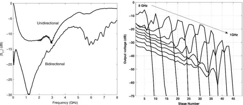
Fig. 12 shows die photographs of both bidirectional and uni-directional RF cochlea chips. In both cases the line or cascade was arranged such that it spiraled inward from the input ter-minal to save space, in a manner reminiscent of the biolog-ical cochlea. Fig. 13 shows the measured input reflection coef-ficient, , of both the bidirectional and unidirectional chips. The matching bandwidth, defined as the frequency range over which 8 dB, was DC to 7.2 GHz for the former and 400 MHz to 3.6 GHz for the latter. The low-frequency limit in the unidirectional case was set by the cut-in frequency of the common-gate LNA. Matching at high frequencies was limited by chip packaging. Packages attenuate high frequency signals because of bond-wire inductances and bond-pad capacitances, which together form low-pass filters.
The bidirectional chip contained stages with . The values of and ranged from 1 nH to 12 nH. Fig. 14
Fig. 13. Measured input reflection coefficients of the bidirectional and unidi-rectional cochlea chips.
Fig. 14. Bidirectional cochlea spatial responses. Output voltage amplitudes were measured from each stage at the following power levels:030; 020; 010; and 0 dBm.
shows the measured frequency-to-space transformation of the bidirectional cochlea at different input power levels. The oper-ating frequency range was approximately 1.2 GHz to 8 GHz, with a measured output noise floor of approximately 82 dBV (rms). As expected, the transfer functions resemble asymmetric bandpass filters, with much steeper roll-offs towards the apical, or low-frequency sides of the peaks. However, they show neg-ative slopes in regions significantly basal to the peaks. This be-havior is due to two reasons: attenuation due to series line loss, and measurement error due to the dead-zone of the EDs, which causes the RF to DC conversion gain to decrease exponentially for stage outputs smaller than 5.5 mV .
Fig. 15. Spatial responses of the bidirectional RF cochlea to exponentially-spaced input frequencies varying between 1 GHz and 8 GHz. The input power level was fixed at010 dBm.
Fig. 16. Spatial responses of the bidirectional RF cochlea at various frequen-cies obtained while varying the value of the active element within each stage. The bias voltageV that sets this negative resistance R was increased from 0.56 V to 0.67 V in 10 mV steps.
Fig. 15 shows measured spatial responses of the bidirectional cochlea to exponentially-spaced input frequencies varying be-tween 1 GHz and 8 GHz, with the input power level fixed at 10 dBm. Fig. 16 shows how the spatial response at various frequencies changes if the value of the negative resistance, is changed by varying the bias voltage . The peak gain in-creases as is increased, decreasing the value of .
Fig. 17 shows spatial responses of the bidirectional cochlea at 10 dB input level for various values of the line loss can-cellation resistance . The value of can be varied by changing the bias voltage . We see that a significant amount of line loss can be cancelled by increasing , which
Fig. 17. Spatial responses of the bidirectional RF cochlea at various frequen-cies obtained while varying the value of the series loss cancellation within each stage. The bias voltageV that sets this negative resistanceR was increased from 0.40 V to 0.58 V in 20 mV steps.
Fig. 18. Measured compression curves of the bidirectional RF cochlea. The spatial location was fixed at the point where maximum response was obtained forf = 5:3 GHz, and the response to frequencies below f was mea-sured at several power levels.
decreases . However, small values of disturb the local impedance, causing unwanted reflections of the traveling wave that show up as secondary peaks in these spatial responses. This effect limits the amount of cancellation that can be applied.
Fig. 18 shows how the peak gain of the bidirectional cochlea responses decreases with increasing input amplitude. These compression curves were taken by observing the response at a fixed location, the best position for GHz, to various input frequencies, including . We see that the response at , being larger, compresses for smaller input power levels than at other frequencies. This behavior is qualitatively similar to that observed in the biological cochlea.
Fig. 19. Measured response of the bidirectional RF cochlea to two simultane-ously applied input frequencies. One input was held fixed at 2.4 GHz while the other was increased exponentially from 1 GHz to 8 GHz (left to right in the figure). The power level of both inputs was held fixed at010 dBm.
Fig. 19 shows a two-tone response: here two input frequen-cies were simultaneously fed into the bidirectional cochlea. One tone was held fixed at 2.4 GHz, while the other was swept expo-nentially with time. The cochlear outputs were monitored as a function of time and plotted in the figure. As expected, the spa-tial response due to the second tone moves linearly with time, while that due to the first remains fixed. Both tones had equal input amplitudes ( 10 dBm). Improvements in frequency res-olution, especially in the presence of noise, can be obtained by using the phase information, such as temporal correlations be-tween stages, present within cochlear transfer functions [33], [34].
Our unidirectional cochlea chip contained stages with . Spatial responses were broadly similar to those obtained from the bidirectional cochlea, but secondary peaks due to inter-stage reflections were absent because of the unidirectional nature of the cascade. This property allows a lower value of to be used, which reduces noise, power consumption and chip area at the cost of frequency resolution. Our usable frequency range is between 600 MHz and 6 GHz. The peak voltage gain and output noise are both higher for this cochlea, resulting in better input-referred sensitivity (approxi-mately 80 dBm over the “best octave”, 2–4 GHz).
Fig. 20 shows spatial responses of the unidirectional cochlea to three input frequencies and four power levels. The frequency-to-space transform is clearly visible, as is gain com-pression at high input power levels. The low-frequency gain of each cochlear stage was slightly less than 1 and could not be increased, for reasons described in Section IV.B. As a result, as the input frequency decreased the peak gain of the cochlear transfer function increased, as expected, but then decreased instead of saturating to a constant value. This behavior explains why intermediate input frequencies, such as the 2.4 GHz tone
Fig. 20. Spatial responses of the unidirectional cochlea to different input fre-quencies at the following power levels:030; 040; 050; 060 dBm.
Fig. 21. Spatial responses of the unidirectional cochlea to two different input frequencies for different values of the gain-control resistorR .
in Fig. 20, have the highest peak gains and display the most gain compression.
Fig. 21 shows that we can control the peak gain of the cochlear transfer functions by changing the value of , the load resistor shown in Fig. 10. The figure shows spatial re-sponses at 2 and 4 GHz for different values of k , where is the digital code of the 5-bit DAC that sets . In this case was increased from 11 to 16, decreasing from 91 to 67 . The result is increased voltage gain. However, power consumption also goes up, because the transconductance of the transistors and inside each filter must increase to keep the gain fixed at 1. In this case power consumption increased from 200 mW to 300 mW.
TABLE I PERFORMANCESUMMARY
Fig. 22. Measured frequency-to-space transform for the unidirectional and bidirectional cochleas, showing the location of the peak response as a function of input frequency.
The performance of both cochleas is summarized in Table I. In the table, peak voltage gain refers to the gain experienced by small signals (no gain compression). In addition, the quoted dy-namic range is for single input tones, with the maximum signal being set by gain compression, and the minimum signal by the input-referred noise floor. The presence of other tones will re-duce dynamic range due to two-tone suppression, which is seen in the biological cochlea and also in our cochlea. Two-tone sup-pression is beneficial in recognizing dominant tones in noisy environments and has led to bio-inspired spectral-analysis algo-rithms that help improve hearing in noise for the deaf [35], [36]. Fig. 22 summarizes the frequency-to-place transform mea-sured for both designs. Deviations from exponential scaling are visible at the low frequency end of the bidirectional design and are caused by the fact that our simple line-termination network cannot perfectly approximate the line impedance at all frequen-cies. A higher order termination network can be used to reduce this effect. Deviations from exponential scaling in the unidirec-tional design were mainly caused by gain compression, which makes it difficult to determine the location of the peak response.
VI. SUMMARY
We have described two real-time, on-chip spectrum analyzers that may be useful for power-and-hardware efficient front ends
in software, cognitive, and ultra-wideband radios. Such radios could use real-time scans of the increasingly crowded RF spectrum to adapt their communication strategies. Our analog RF cochlea chips consume about 100 times less power than that required for direct digitization of the entire bandwidth. By performing initial, high-speed filtering, the chips also decrease the bandwidth and power required for later signal processing, such as the use of more conventional narrowband and hetero-dyning systems to improve the frequency resolution. Our novel rational unidirectional cochlear model can also enable practical audio-frequency silicon cochleas with low group delay and sharp rolloff slopes. Overall, the RF cochlea illustrates that sensory systems found in nature yield architectures that are useful in man-made signal processors. It also provides insight into why the biological cochlea is efficient.
APPENDIX
This Appendix describes our transformer design flow. Unlike resistors and capacitors, inductors and transformers are not stan-dard integrated circuit components, and no models were avail-able. Normally magnetic components are designed by hand, an initial geometry based on an analytical formula being iteratively refined via electromagnetic simulations. While this approach is sufficient for typical RF designs that use a small number of mag-netic components, it rapidly becomes tedious when this number increases. In addition, the mapping from transformer values to geometry is one-to-many, so the final geometry may not be opti-mized for size or quality factor. We decided to automate the de-sign process as much as possible. We used an analytical formula that predicts the inductance value, , as a function of geometry [37] and derived the following formula for calculating the DC series resistance of a -turn spiral:
(29) where is the resistivity of the metal layer, its thickness, and the width of each turn. In addition, each turn is assumed to consist of a regular -sided polygon, and are the di-ameters of the circles that inscribe the outer and inner edges of the spiral, respectively, and . The AC re-sistance can be found by taking the skin effect into account [38]: (30) where , and is the skin depth. We assumed that , the center frequency of the stage, was much lower than the self-res-onant frequency of the coil. Thus, we were able to analytically find the quality factor of the inductor at . We then wrote a numerical optimization routine using Mathematica to find the optimal coil geometry. The routine finds the geometry that produces the required value of while minimizing layout area and also ensuring that is higher than , a constant. Square coils were used because they have the largest inductance for a given layout area. The two coils that form a transformer were laid out on different metal layers; their centers were offset from each other. The amount of offset was varied to control the value of the coupling factor . This process was re-peated for every stage.
An electromagnetic simulator was used to create broadband frequency-domain models, i.e., two-port S-parameters, for each transformer [39]. Next, a model-order reduction routine avail-able in our CAD software (SpectreRF, Cadence Design Sys-tems, San Jose, CA) was used to create lumped equivalent cir-cuit models, suitable for time-domain simulations, from the fre-quency-domain models. Finally, we wrote a MATLAB (The MathWorks, Natick, MA) program to automatically generate on-chip layouts for these optimal transformer geometries.
ACKNOWLEDGMENT
The authors would like to thank the anonymous reviewers for several valuable suggestions.
REFERENCES
[1] R. Sarpeshkar, R. F. Lyon, and C. A. Mead, “A low-power wide-dy-namic-range analog VLSI cochlea,” Analog Integr. Circuits Signal
Process., vol. 16, no. 3, pp. 245–274, Aug. 1998.
[2] J. O. Pickles, An Introduction to the Physiology of Hearing, 2nd ed. London, U.K.: Academic Press, 1988.
[3] C. D. Geisler, From Sound to Synapse: Physiology of the Mammalian
Ear, 1st ed. Oxford, U.K.: Oxford Univ. Press, 1998.
[4] W. E. Brownell, C. R. Bader, D. Bertrand, and Y. de Ribaupierre, “Evoked mechanical responses of isolated cochlear outer hair cells,”
Science, vol. 259, pp. 194–196, Jan. 1985.
[5] P. Dallos, B. N. Evans, and R. Hallworth, “Nature of the motor element in electrokinetic shape changes of cochlear outer hair cells,” Nature, vol. 350, pp. 155–157, Mar. 1991.
[6] P. Dallos and B. N. Evans, “High-frequency motility of outer hair cells and the cochlear amplifier,” Science, vol. 267, no. 5206, pp. 2006–2009, Mar. 1995.
[7] G. Frank, W. Hemmert, and A. W. Gummer, “Limiting dynamics of high-frequency electromechanical transduction of outer hair cells,”
Proc. Natl. Acad. Sci. USA, vol. 96, pp. 4420–4425, Apr. 1999.
[8] J. Ludwig, D. Oliver, G. Frank, N. Klöcker, A. W. Gummer, and B. Fakler, “Reciprocal electromechanical properties of rat prestin: The motor molecule from rat outer hair cells,” Proc. Natl. Acad. Sci. USA, vol. 98, no. 7, pp. 4178–4183, Mar. 2001.
[9] L. Robles and M. A. Ruggero, “Mechanics of the mammalian cochlea,”
Physiol. Rev., vol. 81, no. 3, pp. 1305–1352, Jul. 2001.
[10] C. A. Shera, “Intensity-invariance of fine time structure in basilar-membrane click responses: Implications for cochlear me-chanics,” J. Acoust. Soc. Am., vol. 110, no. 1, pp. 332–348, Jul. 2001. [11] C. A. Shera, “Mammalian spontaneous otoacoustic emissions are
am-plitude-stabilized cochlear standing waves,” J. Acoust. Soc. Am., vol. 114, no. 1, pp. 244–262, Jul. 2003.
[12] T. K. Lu, S. Zhak, P. Dallos, and R. Sarpeshkar, “Fast cochlear am-plification with slow outer hair cells,” Hearing Research, vol. 214, no. 1–2, pp. 45–67, Apr. 2006.
[13] A. Hajimiri, “Distributed integrated circuits: An alternative approach to high-frequency design,” IEEE Commun. Mag., vol. 40, no. 2, pp. 168–173, Feb. 2002.
[14] E. Afshari, H. S. Bhat, A. Hajimiri, and J. E. Marsden, “Extremely wideband signal shaping using one-and two-dimensional nonuniform nonlinear transmission lines,” J. Appl. Phys., vol. 99, no. 5, p. 054901, Mar. 2006.
[15] D. S. Ricketts, X. Li, N. Sun, K. Woo, and D. Ham, “On the self-gen-eration of electrical soliton pulses,” IEEE J. Solid-State Circuits, vol. 42, no. 8, pp. 1657–1668, Aug. 2007.
[16] E. Afshari, H. S. Bhat, and A. Hajimiri, “Ultrafast analog Fourier trans-form using 2-D LC lattice,” IEEE Trans. Circuits Syst. I, vol. 55, no. 8, pp. 2332–2343, Aug. 2008.
[17] G. E. R. Cowan, R. C. Melville, and Y. P. Tsividis, “A VLSI analog computer/digital computer accelerator,” IEEE J. Solid-State Circuits, vol. 41, no. 1, pp. 42–53, Jan. 2006.
[18] R. F. Lyon and C. A. Mead, “An analog electronic cochlea,” IEEE
Trans. Acoust. Speech Signal Process., vol. 36, no. 7, pp. 1119–1134,
Jul. 1988.
[19] A. G. Andreou, “Electronic arts imitate life,” Nature, vol. 354, pp. 501–501, Dec. 1991.
[20] W. Liu, A. G. Andreou, and M. H. Goldstein, Jr., “Voiced-speech rep-resentation by an analog silicon model of the auditory periphery,” IEEE
Trans. Neural Networks, vol. 3, no. 3, pp. 477–487, May 1992.
[21] L. Watts, D. A. Kerns, R. F. Lyon, and C. A. Mead, “Improved imple-mentation of the silicon cochlea,” IEEE J. Solid-State Circuits, vol. 27, no. 5, pp. 692–700, May 1992.
[22] T. Hinck, Z. Yang, Q. Zhang, and A. Hubbard, “A current-mode imple-mentation of a traveling wave amplifier model similar to the cochlea,” in Proc. IEEE Int. Symp. Circuits and Systems (ISCAS’99), 1999, vol. 2, pp. 228–231.
[23] S. Zhak, S. Mandal, and R. Sarpeshkar, “A proposal for an RF cochlea,” in Proc. Asia Pacific Microwave Conf., Dec. 2004.
[24] S. Mandal, S. Zhak, and R. Sarpeshkar, “Circuits for an RF cochlea,” in Proc. IEEE Int. Symp. Circuits Syst. (ISCAS 2006), May 2006, pp. 2845–2848.
[25] C. Galbraith, R. D. White, K. Grosh, and G. M. Rebeiz, “A mammalian cochlea-based RF channelizing filter,” in IEEE MTT-S Int. Microwave
Symp. Dig., 2005, p. 4.
[26] C. Galbraith, G. Rebeiz, and R. Drangmeister, “A cochlea-based pre-selector for UWB applications,” in IEEE Radio Frequency Integrated
Circuits (RFIC) Symp., 2007, pp. 219–222.
[27] C. Galbraith, R. D. White, L. Cheng, K. Grosh, and G. M. Rebeiz, “Cochlea-based RF channelizing filters,” IEEE Trans. Circuits Syst. I, vol. 55, pp. 969–979, 2008.
[28] G. Zweig, “Finding the impedance of the organ of corti,” J. Acoust.
Soc. Am., vol. 89, no. 3, pp. 1229–1254, Mar. 1991.
[29] E. M. Williams, “Radio-frequency spectrum analyzers,” Proc. Inst.
Radio Eng., vol. 34, no. 1, pp. 18–22, Jan. 1946.
[30] S. M. Zhak, “Modeling and design of an active silicon cochlea,” Ph.D. dissertation, Massachusetts Inst. Technol., Cambridge, MA, Sep. 2008. [31] L. Watts, “Cochlear mechanics: analysis and analog VLSI,” Ph.D. dis-sertation, California Inst. Technol., Computation and Neural Systems, Pasadena, CA, Apr. 1993.
[32] S. Puria and J. Allen, “A parametric study of cochlear input impedance,” J. Acoust. Soc. Am., vol. 89, no. 1, pp. 287–309, Jan. 1991.
[33] X. Yang, K. Wang, and S. A. Shamma, “Auditory representations of speech signals,” IEEE Trans. Inf. Theory, vol. 38, no. 2, pp. 824–839, Mar. 1992.
[34] J. W. Wang, R. Sarpeshkar, M. Jabri, and C. Mead, “A low power analog front end module for cochlear implants,” in Proc. XVI World
Congr. Otorhinolaryngology, Head and Neck Surgery, Sydney,
Aus-tralia, Mar. 1997.
[35] L. Turicchia and R. Sarpeshkar, “A bio-inspired companding strategy for spectral enhancement,” IEEE Trans. Speech Audio Process., vol. 13, no. 2, pp. 243–253, Mar. 2005.
[36] A. Bhattacharya and F. G. Zeng, “Companding to improve cochlear-implant speech recognition in speech-shaped noise,” J. Acoust. Soc.
Am., vol. 122, no. 2, pp. 1079–1089, Aug. 2007.
[37] S. S. Mohan, M. del Mar Hershenson, S. P. Boyd, and T. H. Lee, “Simple accurate expressions for planar spiral inductances,” IEEE J.
Solid-State Circuits, vol. 34, no. 10, pp. 1419–1424, Oct. 1999.
[38] T. H. Lee, The Design of CMOS Radio-Frequency Integrated Circuits, 2nd ed. Cambridge, U.K.: Cambridge Univ. Press, 2004.
[39] A. M. Niknejad, ASITIC: Analysis and Simulation of Spiral Inductors and Transformers for ICs. [Online]. Available: http://rfic.eecs.berkeley. edu/~niknejad/asitic.html
Soumyajit Mandal (S’01) received the B.Tech. degree from the Indian Institute of Technology, Kharagpur, India, in 2002, and the S.M. degree in electrical engineering from the Massachusetts Insti-tute of Technology (MIT), Cambridge, MA, in 2004. He is currently working toward the Ph.D. degree at MIT. His research interests include analog and bio-logical computation, nonlinear dynamics, low-power analog and RF circuit design and antennas.
Mr. Mandal was awarded the President of India Gold Medal in 2002.
Serhii M. Zhak received the S.M. degree in physics from the Moscow Institute of Physics and Tech-nology, Russia, in 1999, and the Ph.D. degree in electrical engineering and computer science from Massachusetts Institute of Technology (MIT), Cambridge, MA, in 2008. His research interests include biomedical implants for the deaf, low-power and low-noise integrated analog design, digital and analog feedback and optimal control, power electronics, and integrated radio-frequency circuits. Dr. Zhak is currently with the power management group at Maxim Integrated Products.
Rahul Sarpeshkar (M’97) received the S.B. de-gree in electrical engineering and the S.B. dede-gree in physics from the Massachusetts Institute of Technology (MIT), Cambridge, MA, in 1990 and the Ph.D. degree from the California Institute of Technology, Pasadena, in 1997.
He was with Bell Labs as a Member of the Tech-nical Staff in 1997. Since 1999 he has been on the fac-ulty of the Electrical Engineering and Computer Sci-ence Department at MIT, where he heads a research group on Analog VLSI and Biological Systems and is currently an Associate Professor. He holds over 20 patents and has authored more than 90 publications, including one that was featured on the cover of
Na-ture. His website is http://www.rle.mit.edu/avbs.
Dr. Sarpeshkar has received the Packard Fellow Award given to outstanding young faculty, the Office of Naval Research Young Investigator Award, the Na-tional Science Foundation Career Award, and the Indus Technovator Award. He has also received the Junior Bose Award and the Ruth and Joel Spira Award, both for excellence in teaching at MIT. He is currently an Associate Editor of IEEE TRANSACTIONS ONBIOMEDICALCIRCUITS ANDSYSTEMS. His research interests include analog and mixed-signal VLSI, biomedical systems, ultra low power circuits and systems, biologically inspired circuits and systems, molec-ular biology, neuroscience, and control theory.
![Fig. 3. Normalized BM admittance Y proposed by Zweig [28].](https://thumb-eu.123doks.com/thumbv2/123doknet/14159932.473105/5.891.136.821.98.729/fig-normalized-bm-admittance-y-proposed-zweig.webp)