I
Bandgap Current Source
by
Matthew C. Guyton
B.S.
Electrical Engineering
University of Maryland, College Park (2000)
Submitted to the Department of Electrical Engineering and Computer Science
in partial fulfillment of the requirements for the degree of
Master of Science in Electrical Engineering and Computer Science
at the
MASSACHUSETTS INSTITUTE OF TECHNOLOGY
September 2002
@ Massachusetts Institute of Technology 2002. All rights reserved.
A uthor ...
...
Department of Electrical Engineering and Computer Science
August 31, 2002
Certified by...
Accepted by...
Hae-Sung Lee
Professor of Electrical Engineering
Thesis Supervisor
...
...
Arthur C. Smith
Chairman, Department Committee on Graduate Students
Department of Electrical Engineering and Computer Science
BARKER
MASSA CHUSETTS INSTITUTE OF TECHNOLOGY
Bandgap Current Source
by
Matthew C. Guyton
Submitted to the Department of Electrical Engineering and Computer Science on August 31, 2002, in partial fulfillment of the
requirements for the degree of
Master of Science in Electrical Engineering and Computer Science
Abstract
Most analog circuits require reference voltages and currents that do not vary with power supply voltage and temperature. The typical solution to this problem is the 1.2V bandgap voltage reference. However, producing non-integer multiples of this voltage, or a bandgap current reference from this voltage source, requires an operational amplifier. The use of an op-amp leads to increased power consumption and design complexity.
The focus of this research is to develop a simple low-power current reference that is independent of temperature and power supply voltage. We have developed a novel bandgap core circuit that produces a bandgap referenced output current directly without an opera-tional amplifier. The same core circuit can also be used to generate arbitrary non-integer multiples of bandgap voltage.
A prototype 2-terminal bandgap current source has been designed and fabricated
em-plying only 4 MOS transistors and 2 parasitic PNP transistors in a standard 0.35pm CMOS technology. Although it is clear that the design has not yet been optimized, initial results show temperature and power-supply independence comparable with commercial standards. Thesis Supervisor: Hae-Sung Lee
Acknowledgments
Thank you to the family and friends who stood by me, the labmates who put up with my neverending stream of questions, the advisor who was willing to teach me, the brothers who took care of me even when I was sick, and the God whose love they exhibited towards me.
Contents
1 Introduction 1.1 Background 1.2 1.3 Typical Solution . . . . Thesis Motivation . . . . 2 Topology2 1 Im leomentatinn of RPeistnr Ratin
2.2 Startup Condition 2.3 Stability . . . . . 3 Simulation 3.1 Ideal Resistors 3.2 Poly2 Resistors 4 Layout 4.1 MOS Transistors 4.2 Resistors . . . . . 4.3 BJTs . . . . 4.4 Test structures 5 Testing 5.1 Setup . . . . 5.2 Results. . . . . . 6 Conclusion 6.1 Difficulties Encountered . . . . 6.2 Future W ork . . . . A Full Schematic B PC Board
C BJT Extraction From Layout
13 . . . . 13 13 13 17 19 19 19 25 25 25 29 29 29 31 31 35 35 35 39 . . . . 39 . . . . 40 41 43 47 . . . . . . . . . . . . . . . . . . . . . . . . . . . . . . . . .
List of Figures
1-1 Typical bandgap current source [1, Fig. 4.50]. . . . . 14
2-1 Base design for simple low-power bandgap current source. . . . . 18
2-2 Sub-circuitry used to vary RI, and therefore resistor ratio K. . . . . 20
2-3 Node voltages for zero-current state. . . . . 21
2-4 Feedback stability analysis. Dotted lines indicate alternate configuration. 22 3-1 Simulation sweep of Isink vs. temperature (using ideal resistors). . . . . 26
3-2 Simulation sweep of Isink vs. voltage applied (using ideal resistors). . . . . . 27
4-1 Com plete layout. . . . . 30
4-2 Layout of PMOS current mirror transistors, MI and M2. The gates of these transistors are tied together (not shown). . . . . 31
4-3 Layout of NMOS voltage mirror transistors, M3 and M4. . . . . 32
4-4 Resistor array and MOS bypass switches. . . . . 33
5-1 Chip 2 - Isink vs. Vapp. . . . . 36
5-2 Chip 4 - Temperature sensitivity = 113 ppm/deg C . . . . 37
A-1 Complete schematic. . . . . 42
B-1 Test setup - printed circuit board schematic. Note that pins 21-40 of the DIP are part of a different project. . . . . 44
B-2 Test setup -printed circuit board layout. Board is split. Everything to right of DIP40 package placed outside temperature controlled environment. . . . 45
List of Tables
5.1 Temperature sensitivity for different resistor ratios . . . . 36 5.2 Summary of results for bandgap current source . . . . 38
Chapter 1
Introduction
1.1
Background
A voltage or current source is an essential block of many circuits. For example, in A/D converters this source would be used as a comparative reference. For a given analog input level, an ideal A/D converter will always give the same digital output, independent of external conditions such as temperature and power-supply level. Thus it would make sense to use a source reference that does not depend on these two factors. Many analog circuits also require biasing that does not depend on these factors.
1.2
Typical Solution
Most analog circuit textbooks [1, p.345] cover the design of a bandgap voltage source that is temperature independent and in some implementations, power-supply independent as well. The bandgap source relies on the well-characterized and effectively linear dependencies of base-emitter voltage (negative dependence) and thermal voltage (positive dependence) on temperature. Using resistors to ratio each component's effect on the output voltage, these two temperature dependencies are cancelled, creating a temperature-independent 1.2V supply.
A temperature-independent current reference can be created from the bandgap voltage source, typically using an op-amp. If necessary, this current reference can then be used to create non-integer multiples of the original 1.2V supply.
Figure 1-1 shows a typical bandgap current source design which uses an op-amp and resistor to generate a current source using the bandgap voltage, V0
st,
as a reference. Notethat the temperature dependence of resistor R2 must be taken into account in the resistor
ratio x.
This design is not suitable for low-power applications because power is wasted in biasing the op-amp and the three transistor columns used to set up the bandgap voltage. Another problem is that this is a three-terminal device, which adds to design complexity.
1.3
Thesis Motivation
Our goal is to design a simple low-power current source that is independent of temperature and power-supply. To meet the desired goal of simplicity, our design should use as few transistors as possible (and therefore should not require op-amps). We will also pay careful
Vdd Ml M2 M5 M6 M7 Ms M3 M4 RI 12 M9 M10
Vt current
Isink + Ml R1*x R2attention to the use of biasing current to minimize power consumption requirements. For simplicity of usage, a two-terminal implementation is being sought.
Chapter 2
Topology
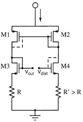
The basic design is shown in Figure 2-1. Mi and M2 act as a current mirror. R2 and R3
are the same size. The saturation current of Q2 is larger than that of Qi by a factor S.
Start-up circuitry is not shown.
Note that this is a two-terminal device that uses no op-amps in the design. Also, no bias current is wasted because all transistors are in the path of sin.k
The gate-source voltages for M3 and M4 are equal because they have the same drain
current (from the M1
/M
2 current mirror). It is assumed that Early effect can be neglecteddue to long channel-lengths. Thus, the voltage across both R2 and R3 will be equivalent to
the base-emitter voltage of Qi and so these two resistors will carry the exact same quantity of current.
The current through R1 is a function of the difference between the base-emitter voltages
of Q1 and Q2. Thus this current is AVBE dependent. In a BJT:
VBE = VT ln(Ic/Is)
Note that Qi and Q2 have different saturation currents. Let: S = Is2/isI
From the current mirror:
ICI + IR3 = IC2 + IR2
But since R2 and R3 are equivalent and have the same voltage (VBE1) across them:
IR2 = IR3
And so:
ICI = IC2
Thus:
AVBE = VBE1 ~ VBE2 = VT In( ICIS2 =VTInS
IC21Sl
Thus the current that is proportional to AVBE is also proportional to thermal voltage, VT.
'sink
Ml
M2
M3
M4
AVI,RI
R2
Q1
Q2
Let K be the resistor ratio needed to cancel out temperature coefficients.
Then the amount of current sunk by this circuit is determined only by the value of the unit resistor R1:
Isink 2 VBEl + AlVBE
(2.1)
2 (VTln(Ic1/Isi) V ln S) K R1 R, 2VT VT inS 2VT i In + In S KR1 IsiR1 ) R
It can be seen that, to a first approximation, none of the parameters depend on VDD and that current can be set by determining R, (and therefore R2) to solve the transcendental
equation above for the desired value of current.
2.1
Implementation of Resistor Ratio
Resistor ratio K is set by bypassing sections of resistor R, via MOS switches M5 - M12 (Figure 2-2).
2.2
Startup Condition
As is typical for self-biased circuits [1, p.326], this topology has two stable states of operation
- the desired state and a zero-current state. The node voltages that make the zero-current state possible are shown in Figure 2-3.
Startup circuitry was not included on-chip to minimize complications from extra com-ponents. Because every major node of the circuit was connected to a pin, any necessary startup circuitry could be connected externally.1
2.3
Stability
Because self-biasing circuits rely on feedback, care must be taken not to create an unstable loop.
Suppose a positive disturbance is introduced at the gate of M4. This disturbance
in-creases VGS4, which increases ID4- The increase in ID4 is mirrored through M1
/M
2,in-creasing the gate voltage of diode-connected M3. However, the gate of M3 is shorted to the
gate of M4, and so a positive feedback loop is created. For this feedback loop to be stable,
AVG3 AVG4
'It turned out that any small disturbance pushed the circuit out of the zero state and so startup circuitry was not needed for lab testing.
3R 9R R
Switch 1 % -
M5 4R RSwitch 2%
M6 3R/2 RSwitch 4%
|
M7 R/4 RSwitch 8%
|
M8 R/2 RSwitch 16%
|
M9 R RSwitch 10%1,-
M10 RSwitch
10%2
-1
Mi RR1
=
10*R
sink 0 VDD
Ml
M2
VDDM3
M4
0
0
00
ORi
R2
Q1
Q2
Ml
M2
M3
vM4
R
R'>R
Figure 2-4: Feedback stability analysis. Dotted lines indicate alternate configuration.
Consider the circuit shown in Figure 2-4, which is a modified form of Figure 2-1.
qlC
'm - kT
Because of current mirror M1
/M
21Cl 1 C2 grnl m 9m2
Comparing Figure 2-4 with the original Figure 2-1, it is clear that:
and so we meet our stability condition
AVG3 Vout 1--m RI
=_ _ = <1
AVG4 Vdist 1 + gmfR'
However, if the circuit is rearranged such that, instead of M2 and M3, Mi and M4 are
diode-connected (see dotted lines in Figure 2-4), then the gain of the positive feedback loop is greater than unity, causing the circuit to be unstable. In practice, such a circuit would most likely latch upon startup.
Chapter 3
Simulation
The circuit was simulated using model file data downloaded from the MOSIS website as part of the TSCM 0.35pm 2-poly process design kit. This data was formatted for the Spectre simulator, and so Spectre was used for simulations. This choice was also appropriate because of Spectre's native support for temperature sweeps.
3.1
Ideal Resistors
Initial simulations were done using ideal resistors (no temperature dependence). Results for a resistor ratio K=25kQ/4.lkQ and a BJT saturation current ratio S=20 are shown in Figure 3-1.
As can be seen in the Cadence graphs, the VT component of sink increased with temper-ature, while the VBE component decreased with temperature. The sum of these two com-ponents created a 100pA current source which was temperature independent until about
1000C.
A sweep of VDD (Figure 3-2) gave an output impedance of better than 100 kQ (in other words, an output admittance of less than 10 pS). This output impedance came from the increase of the VT component of sink 1. Also note that turn-on voltage for this circuit was approximately V0,=2V.
3.2
Poly2 Resistors
Simulation with modelled Poly2 resistors (TCF=1070ppm) required a resistor ratio, K, of approximately 25kQ/2kQ to create temperature independence. The lower required value of R, can be explained as follows: the resistance of poly2 increases with temperature, which, as seen from equation 2.1 would make the TCF of 'sink more negative. To cancel this
decrease, we need to have a larger PTAT component of current, and thus R1 must be decreased appropriately.
dlsink/dTemp 140n . P 1 10n 80.0n 0. E a 50.0n C 20.On -10 .0 n I , . .. . . . . . . . . .. -30.0 30.0 90.0 150 temp(C)
Contributions of Vt and Vbe components to Isink J
-: Vt component
70u .: Vbe cornponent
60u I 50u 40u 3 u .. ... ... .... .. . .... .. .. -30.0 30.0 90.0 150 temp ( C ) DC Response 98.30u : ink 98.00u 97.70u c 97.40u
0.0 Output Admittance
/
3.0 6.0 Vdd(V) 9.0Contribution of Vt and Vbe components to Isink Vt component
60u Vbe com ponent
40u 20u-0 20u-0 . 0.0 3.0 6.0 Vdd(V) 9.0 DC Response 5 200u a: isink -.--- a-0.0 3.0 6.0 Vdd(V) 9.0
Figure 3-2: Simulation sweep of Isink vs. voltage applied (using ideal resistors).
40u 30u 20u 1 0u 0.0 -o -o U 0) j C.-) 12 12 150u 100u 50.Ou a: 0.) n C-) 0.00 12
, .
.
Chapter 4
Layout
The test circuit was fabricated via MOSIS using TSMC's 0.35um process. The complete layout is shown in Figure 4-1
4.1
MOS Transistors
Because the operation of this circuit relies on the precise cancellation of components, match-ing is of absolute importance.
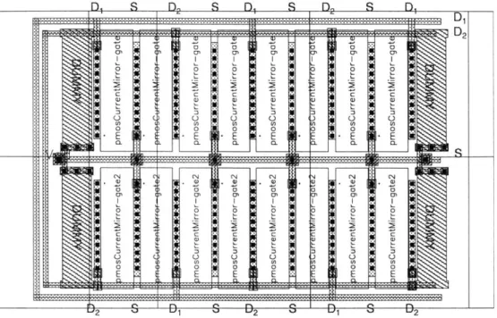
To achieve this matching, the MOS transistors were laid-out in cross-coupled pairs of transistor fingers [2, p.435]. The PMOS current mirror transistors, Mi and M2, were laid
out in the pattern di-s-d2-s-di-s-d2-s-di
/
d2-s-di-s-d2-s-di-s-d2, where the source was sharedbetween the two transistors (Figure 4-2).
Dummy transistors were included on the ends of each row so that each MOS finger would be as uniform as possible.
The NMOS voltage mirror transistors, M3 and M4, were laid out in a similar format
(Figure 4-3). However, because M3 and M4 have electrically distinct source nodes, this
layout was a bit more complicated, and folded gate configurations were used for the unit transistor (as opposed to simple fingers).
4.2
Resistors
Resistors were created in the Poly2 layer as an interdigitated array of resistor sections (Fig-ure 4-4). Polysilicon was chosen because its sheet resistance (48.6Q/sq) was high enough to allow for reasonable geometries of kQ-range resistors and because its temperature depen-dency was well-characterized (process specifications state 1070 ppm).
An attempt was made to layout all resistor sections around a common centroid. In each resistor segment, resistors were connected in alternating directions to cancel thermoelectric effects (mismatch due to thermal gradients) [2, p.240,251]. Dummy resistors were used to ensure uniform etching of all electrically significant resistor segments.
The unit resistor was 3.75 squares, which gave a unit resistance of
R = 3.75sq * 48.6Q/sq = 182.25Q
R2 and R3 each consisted of 122 of these unit resistors in series (22kQ). R1 consisted of
NMOS Voltage Mirror I- I I Resistor Array
I
PMOS Current . Mirror I I I I A s i k A k-. A- k- vkkA -zs A -k -N , Z. lk -N -N ,N INN i ,s S.11 Z k V kA k N7 N vo N -, v -N N -Q0 &V ;:k kAi M-k , N :% 7 S \: ,s N ;ZIN 'S :A, Ak- -k v A Q xN &V ;.-,v "0, w- sx I- N -,v Ai ik-: k V -k v A-z' ;A &4 41, W v, o", NNiA -- N zk % N;z INN ,Figure 4-2: Layout of PMOS current mirror transistors, transistors are tied together (not shown).
M1 and M2. The gates of these
switches. Other MOS switches were used to open alternate current paths, decreasing R1 in increments of 1, 2, 4, 8, and 16%. The total set of MOS switches allowed a test range for the resistor ratio, K, of 69%-130% of the baseline value.
4.3
BJTs
Qi
is a unit BJT. Q2 is 20 of these unit BJTs in parallel, arranged around Qi on the layout. Dummy BJTs were placed to make sure that all BJTs used in the circuit were surrounded by other BJTs on all sides in the layout.4.4
Test structures
An extra BJT and a 10-unit resistor chain were included on the chip as test structures.
D. S M S ... D, S D2 S D. ... D , ... ... ... ... -- --- --- ... .... ---- -- -- ---D 2 0 0 C3 0 0 0 CP (3) In C, (31 0 0 0 0 0 C C C C Q) Q) Q) W a) n :3 :3 :3 :3 n U W W V) V) W W 0 0 0 0 0 0 E E E E E E C1. a- a CL Q_ T 1- S-i .......... . ... -- --- - -l- --- ... --- ... ---CI4 CN N CIj Q) Q) Q) U 0 a 0) 0 0 0 0 0 C C C C C: CU a) W Q) Q) U y U U C) M U) (n V) U) 0 0 0 0 0 0 E E E E E E rF% C, I r*% n r% n 2 %J L1 12 %J L1 0 02
Se S4 .1D
I I E
I -tic
KOK;"e WEM Hlil
jj, lf
|
id! !!if 1111 iV ll , ONO Dummy Row 4 3 4 3 3 4Dummy Row
I
Figure 4-4: Resistor array and MOS bypass switches. tit F313 7 7i jj
m
A.;
-.. --- .. --7-7L
Chapter 5
Testing
5.1
Setup
In an effort to create a low-cost test setup, a "Hot/Cold Snack Box" from Sharper Image (model #SI712BLU) was used. This box used a Peltier device and could establish a temper-ature environment of 100C - 500C. Because this box created a lot of electrical noise, data
was only taken during passive cooling/heating phases; in other words, the box was turned off once it reached a temperature extreme, then data was taken as the box temperature settled back to room temperature.
The instruments used to take the test data were a Keithley M1321 Thermocouple and an HP 4140B pA Meter. The two instruments were controlled using a computer running LabView 5 through a modified version of code that was originally written by Ching-Chun (Ginger) Wang.
The schematic for the test setup can be seen in Appendix B. Because electrostatic discharge (ESD) protection for the MOS bypass switches (M5 - M1 2) was unfortunately
neglected in the layout design, external capacitors and resistors were used.1
5.2
Results
The test BJT had a DC current gain 3=6 and a saturation current of 2x10' 7A. The test
10-unit resistor had a resistance of 3kQ which gives us a fabricated unit resistance of 300 Q (expected value was R=182.25 Q).
Results from a sweep of applied voltage are shown in Figure 5-1. The chip had a turn-on voltage of about 2V, at which point it exhibited an output resistance of
3.19V - 2.19V
Rom == 350kQ
89.7 p A - 86.9 pA
Also note that the positive feedback caused hysteresis, where the applied voltage would have to drop slightly below the turn-on voltage of 2V (down to about 1.5V) to get the device to turn off.
Next a temperature sweep was done to test the temperature dependence of the current source. Results for different resistor ratios are shown in table 5.1.
I vs. V sik app (taking data w/ V appincreasing/decreasing)
90
1 1.5 2
V app(V)
2.5 3 3.5
Figure 5-1: Chip 2 - Isink vs. Vapp.
... Increasing V Decreasing O ___ app 80 -70 -60 -50 ~40 -30 I 20 10 01*4 0.5
Chip 4 - 100 Minutes Passive Heating/Cooling - All Grounded
10 15 20 25 30
temp(deg C)
35 40 45 50 55
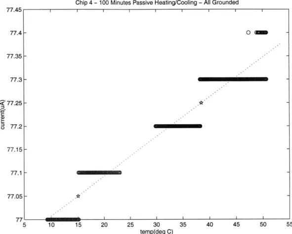
Figure 5-2: Chip 4 - Temperature sensitivity = 113 ppm/deg C
The circuit exhibited the most temperature independence when the gates of all the MOS switches were grounded (RI at maximum). Plots for this configuration are shown in figure
5-2.
Using the box method to characterize the chip's temperature sensitivity gives us the
following:
SIsinkmax - Isink,min 77.3pA - 77.1pA 6 =
ATIsink (380C - 150C)77pA
A summary of results appears in table 5.2. 77.45 77.4 77.35 77.3-77 7 .25 7.2 -m -- -- -- - III 77.15-77.1 77.05 77 5
Table 5.2: Summary of results for bandgap current source
Parameter Magnitude
Output Current (Isink) 77pA Turn-On Voltage (V0,) 2V
Temperature Coefficient (TCF) 113 ppm/0C Tested Temperature Range 100C - 500C Output Impedance (Ro0,) 350 kQ
BJT Saturation Current Ratio (S) 20 Optimum Resistor Ratio (K) 122/13
Chapter 6
Conclusion
A prototype 2-terminal bandgap curent source was designed and fabricated using only 4 MOS transistors and 2 parasitic PNP transistors in a standard 0.35pim CMOS technology. The baseline current of this circuit was 77pA. This is lower than expected in simulations, most likely because the fabricated unit resistance was much higher than the simulated (extracted) resistance. One cause of this discrepancy is the lack of accounting for contact resistance in the extraction rules. Given that each resistor segment was only 3.75 squares, neglecting the contacts significantly underestimates the value of the resistor.
The circuit exhibited a temperature coefficient of 113 ppm/0 C. Commercial bandgap references typically have dependencies of 25-50 ppm/0C. Considering that the circuit ex-hibited the least temperature dependence when R1 was greatest, it is likely that the most efficient resistor ratio was not implemented. Future chips should allow for a much larger value of R1.
Power-supply voltage independence was also exhibited. Output impedance was approx-imately 350 kQ.
6.1
Difficulties Encountered
Extracting BJT data from the layout proved to be difficult because the BJT extraction rules in the design kit from MOSIS were incomplete. The completed rules are documented in Appendix C.
A limitation of using the pA meter was that it had an accuracy of only 3 significant digits. With this level of accuracy, measuring a temperature coefficient close to commercial levels would have required either a) a test environment with a wider temperature range (not practical), or removal of the baseline current before Isink was measured by the ammeter. A PCB implementing the second solution, with a current source in parallel with the ammeter, is shown in Appendix B. However, this solution has yet to be implemented.
A mistake was made in that no electrostatic discharge protection (ESD) was included for the gates of the MOS switches (M5 - M12). During testing, 5 chips were blown. In every
failed chip, the gate of M12 appeared to be shorted. It is not certain why this particular
6.2
Future Work
Potential revisions of the layout should include ESD protection for the gates of the MOS switches, and should allow for a higher resistor ratio.
In order to get higher accuracy, future measurements will use an external current source to cancel out the baseline current, as seen in the schematic of Figure B-1.
Appendix A
Full Schematic
1sink Bcndgap Current Source Matt Guyton
7/31/02
all
in parallel with M1 oil in parallel with M2Ue2 21 in, M19j~ Wa if &k Ml Ilk Wiln M2 1.i 1. ai 15 sn 1 e M7 i
,ldd" .WN
.-200. -200. Gy-2W.u DGy-2 0 29'1' DO3 '1 114 - e -0e -0e -0
R12 veme -U , R 1 dumnye345 -133 R2-, .w- P .2 nlt23 nR142 R In Rt(II!) I4 U; ."~o(1) it net24 wISt247 .. U242 ..t247 RIO R4r.4267 R17 al 2 t244 resistor ratio -""' :'3''' tn -122/13 r4.*~r""/~r"" 05- e .4. Por(-M)APor(-w ) l ""3BJT ratio 2011 8.6 iP Pfef0'1")/Por("w") ,2 03 04 a Q7 - 5 1 1 51 0 12 1 0 1 8 2 gn
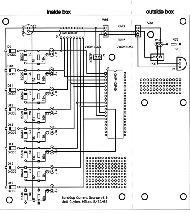
Appendix B
PC Board
For future testing of the bandgap current circuit, a printed circuit board (PCB) has been designed. It implements 2 ideas that have not yet been tested - protection diodes for the gates of the MOS switches (M5 - M1 2), as well as having a current source in parallel with
I
I
I
- 0.PP
03 OLD A: LJ.Od V v£ NO L 11 ,- Utz EEL z rE~'~
'2~x
1d.Th0
nLGLO
£a
98
0 zI
0 C-) U-m -9-60 10 L ED £30L -9--- 14-Z1 LO-a 98-9-
-44--________~~ ____ AAA E z Z F, NE-q t.E I I 0 -riInide
bmK
Ioutsde bak
Vdd HBDIU"@"3
-.a:. 0 -D9 DIODE 2 D10 DIODE D12 E-DIODE C D12-J
DIODE D13E~J
DIODE D14 DIODE in rn D15 DIODE m D16 DODE5
E
I
I
GND Vee N OT U10
00
0
-0
o
o
0
o
0
o
o
o
o
0 0 0 0 00
0
0 0 0 o 0 o 0 0000000000000 0000000000000 0000000000000 0000000000000 0000000000000 0000000000000 0000000000000 0000000000000 0000000000000 0000000000000 ent Source v.0 ISLee, 8/23/020
0000000000000 0000000000000 0000000000000 0000000000000 0000000000000o
0
0
0
Figure B-2: Test setup - printed circuit board layout. Board is split. Everything to right of DIP40 package placed outside temperature controlled environment.
- .~1=1,
~LI
0
BondGap Curr
Matt Guyton,
Appendix C
BJT Extraction From Layout
Getting DIVA to extract the BJT's from the layout proved difficult because the TSMC .35pm design kit came with incomplete rules for this extraction. Glenn Jennings at MOSIS was particularly helpful in debugging this problem. His correspondence is included below.
On Tue, 18 Dec 2001 mcguytonOMIT.EDU wrote:
[ I'm using your 2p4m .35um TSMC process in Cadence.
[
I can't get vertical PNPs to extract as anything (only the metal is[ extracted). Even if I make a cellview containing only your
[
parameterized pcell\pnp, the extraction doesn't recognize it as a BJT![ I can get resistors, PMOS, and NMOS to extract correctly.
[ The error message is "WARNING - no devices available to which
[ properties can be added." Sometimes it says "parameters" instead of
[ "properties".
[
How can I get this to extract correctly?OK, this one first. Make a copy of the original file
cmosp35.3.0/dfII-lib/cmosp35/divaEXT.rul
and do some editing to the copy as follows:
locate this line:
pnpEmitter=geomGetTexted(pdiff "device" "emit" "emitter") and change it to:
pnpEmitter=geomGetTexted(pdiff ("device" "all") "emit" "emitter")
locate all of the following lines, and unmask them:
"pnp ivpcell cmosp35")
; saveRecognition(pnpVertical "nwell")
; sub=geomr(sub subDevices)
; sub=geomStamp(sub pohmic)
; nwell=geomStamp(nwell geomCat(nohmic nohmicPnpBase) error)
; pnpBase=geomStamp(pnpBase nohmicPnpBase)
; pnpEmitter=geomStamp(pnpEmitter pdiff)
; emitterAreaVertical=measureParameter(area (pnpVertical over pnpEmitter)
1.0e-02)
; baseAreaVertical=measureParameter(area (pnpVertical) 1.2755102e-03) ; saveProperty(pnpVertical "model" "pnp")
saveParameter(emitterAreaVertical "area") saveParameter(baseAreaVertical "areab")
This should get you a little farther as far as extraction is concerned. Next is this one:
[ I can't get vertical PNPs (a pcell included with the design kit) to
[ pass DRC. I'm using them diode-connected and so the base (Nwell) is
[ connected to the collector (substrate). It seems that to pass DRC,
[ all Nwells have to be connected to Vdd, otherwise I get the error
[ "substrate soft connected". If the base and collector are shorted, it
[ is not possible to satisfy this rule.
[ How can I do to fix this? It doesn't seem like NWells should have to
[ be tied to Vdd to pass DRC...
This kind of softconnect "error" has to be interpreted by the
designer. In this case, since it is a PNP structure, you should simply disregard it. I fear that tweaking the DRC file to make this
suprious flag go away, would cause more problems than it solved.
Regards,
![Figure 1-1: Typical bandgap current source [1, Fig. 4.50].](https://thumb-eu.123doks.com/thumbv2/123doknet/14142619.470652/14.918.193.728.355.775/figure-typical-bandgap-current-source-fig.webp)