Does p-type ohmic contact exist in WSe[subscript 2]–metal interfaces?
27
0
0
Texte intégral
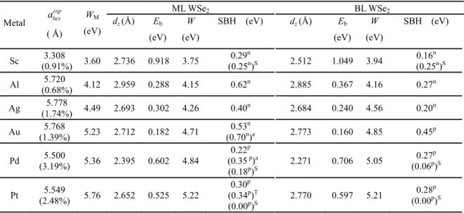
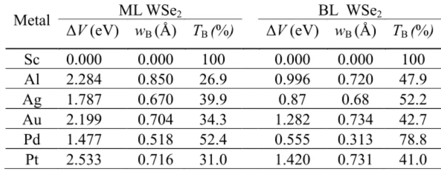
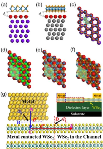
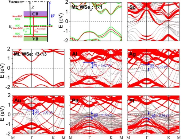
Figure
+7
Documents relatifs