HAL Id: hal-01692046
https://hal.archives-ouvertes.fr/hal-01692046v2
Submitted on 4 Jul 2017
HAL is a multi-disciplinary open access
archive for the deposit and dissemination of
sci-entific research documents, whether they are
pub-lished or not. The documents may come from
teaching and research institutions in France or
abroad, or from public or private research centers.
L’archive ouverte pluridisciplinaire HAL, est
destinée au dépôt et à la diffusion de documents
scientifiques de niveau recherche, publiés ou non,
émanant des établissements d’enseignement et de
recherche français ou étrangers, des laboratoires
publics ou privés.
TCAD Simulation of the Single Event Effects in
Normally-off GaN Transistors after Heavy Ion Radiation
Moustafa Zerarka, Patrick Austin, Alain Bensoussan, Frédéric Morancho,
André Durier
To cite this version:
Moustafa Zerarka, Patrick Austin, Alain Bensoussan, Frédéric Morancho, André Durier. TCAD
Simulation of the Single Event Effects in Normally-off GaN Transistors after Heavy Ion Radiation.
RADECS 2016 (RADiation Effects on Components and Systems), Sep 2016, Brême, Germany. 4p.,
�10.1109/TNS.2017.2710629�. �hal-01692046v2�
TCAD simulation of the Single Event Effects
in
normally-off GaN transistors after heavy ion radiation
M. Zerarka
a,b*,
P. Austin
b, A. Bensoussan
a, F. Morancho
b, A. Durier
aa
IRT Saint Exupéry, 118 Route de Narbonne, 31432 Toulouse, Toulouse, France
b
LAAS-CNRS, Université de Toulouse, CNRS, UPS, Toulouse, France
Abstract— Electrical behavior of normally-off GaN power transistors under heavy ion stress radiation is presented based on 2D-TCAD numerical simulation in order to better understand the mechanism of Single Event Effects (SEE) in these devices.
Keywords— power transistor; GaN; EPC; SEE; sensitive volume ; radiation; heavy ion; TCAD; simulation
I. INTRODUCTION
The use of Gallium Nitride (GaN) power switches is very promising because this material is a more efficient semiconductor than Silicon (Si) or Silicon Carbide (SiC) in terms of "ON-resistance / breakdown voltage" trade-off, which is the most important figure of merit for a power switch. Indeed, the main benefits of this materials are a good functionality at high frequency applications due to its high electron velocity with high power due to the high critical electric field. Specifically the normally-off GaN power transistor could be an attractive candidate for space and aeronautic power applications.
The use of these devices in such environment cannot be ensured without careful consideration of the effects of radiation. Natural Radiation Environment (NRE) is composed of particles of various nature and energy such as heavy ions which can cause the destruction of these devices. Single Event Effects (SEE) is one of the catastrophic effects which could cause normally-off GaN power devices to fail in space systems. Few studies have been carried out to understand SEE in normally-off GaN power transistors.
The objective of this paper is to investigate by 2D TCAD simulation the mechanism of failure induced by heavy ion irradiation on commercial normally-off GaN power transistors (from EPC, Efficient Power Conversion) in order to better understand the electrical behavior after radiation and suggest an explanation of the mechanism of Single Event Effects (SEE) for this devices.
II. TESTVEHICLES
A reverse engineering was carried out on samples GaN EPC2019ENG 200V in order to define the technological parameters of these devices. Fig. 1 gives a cross-section view of the EPC2019 GaN HEMT that will be simulated. The structure consists of a substrate (silicon), a nucleation region comprising different AlGaN layers with aluminum rates gradually decreasing, an unintentional doped (UID) GaN buffer
layer, an AlGaN barrier layer, a p-doped GaN layer [1] and a SiN passivation layer..
Fig. 1. Cross-section view of the active region of the GaN EPC 2019 transistor
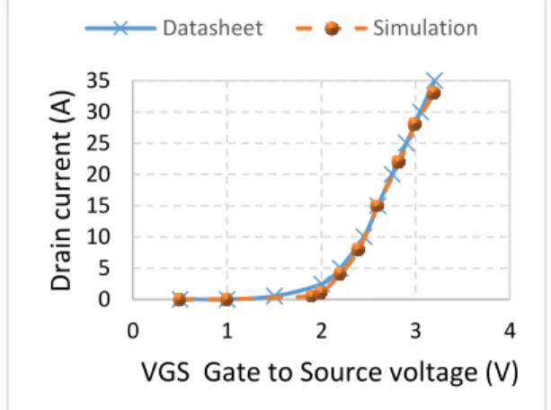
Despite the reverse engineering, some parameters always remain unknown such as intentional and unintentional dopings, carrier mobility, concentration and energy of traps. However, it is necessary to first validate the physical and geometrical parameters obtained thanks to the reverse engineering of EPC2019 transistor and calibrate by simulation those lacking, based on the experimental electrical characteristics of the device. Simulations were carried out with SENTAURUS TCAD simulator [2]. As shown in Fig. 2, the IDS (VGS) transfer
characteristics of the simulated structure match the ones experimentally measured [3].
Fig. 2. Experimental (datasheet) and simulated IDS(VGS) transfer
characteristic IDS of the 200V EPC2019 GaN HEMT.
Source Gate a Drain a Si a GaN buffer a
Transition layers (AlGaN)
0 5 10 15 20 25 30 35 0 1 2 3 4
D
rai
n
cur
rent
(A)
VGS Gate to Source voltage (V)
Concerning the off-state, manufacturers of GaN components do not provide accurate characteristics. Dislocations in the crystal lattice from the manufacture create randomly leakage currents for each device. Two components of the same type can exhibit significant differences in terms of breakdown voltage. EPC2019 devices have been tested to determine the actual values of their breakdown voltage: we found that the same component may give different values (between 200V and 420V) when test was repeated under the same conditions. This can be explained by the heating effect which changes the traps energy after each test. In simulation, the value of the breakdown voltage was adjusted to 450V by fitting some key parameters as the traps in the GaN buffer layer and their energy level.
III. CONDITIONS OF SIMULATIONS WITH HEAVY ION
All simulations were performed in the off-state with different LET (linear energy transfer) and different source-drain bias (40V, 200V, 300V and 400V).
The ionizing impact is simulated by a function allowing the generation of electron–hole pairs in a specific area of the structure. The generation rate of the created charges is described by spatial and temporal Gaussian functions [2]. The track radius is set to 0.05μm, the initial time of the charge generation is 3.10-13s and the temporal Gaussian function width
is 2.10-12s. Detailed work on the modeling of the ion track
charge and energy distribution can be found in the works of H. Dussault et al. in [4] [5].
IV. SIMULATION RESULTS AND DISCUSSION
A. Single Event Transient mechanism
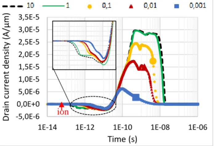
Results in Fig. 3 and 4 show the evolution of the drain current as a function of time following an impact ionizing for different LETs from the front side. Whatever the conditions (LET and bias), all failures are transient and the triggering current can not be sustained. This transient current represents the charge enhancement. Generally, in HEMTs heterostructures, the charge enhancement mechanism is associated to two mechanisms: the bipolar and the back-channel effects. After an ionizing impact by heavy ion, electron–hole pairs are generated, creating ionized plasma. Electrons flow toward the drain contact with high mobility, leading to an excess of holes in the GaN buffer layer, thus electrons are injected to compensate from the source, leading to the switch of the parasitic bipolar transistor. The second charge enhancement mechanism is due to the positive charge accumulation under the gate that serve to reduce the potential barrier between the source and the channel allowing the injection of electrons from the source to the drain via the channel [6] [7]. In Fig. 3 the transient drain current reaches a saturation value for LET of 1 pC/μm. These LET correspond to the maximum of charge which can be generated in the GaN buffer region at 300V. From this amount of charge, the amplitude of transient drain current is constant, whatever the LET value. The saturation value depends especially on the bias voltage and not in the energy or range of the ion. Fig. 4 confirms that the amplitude values can be multiplied by increasing the
drain-source bias voltage for the same charge deposited by the heavy ion.
The transient current have a negative current, just after the impact (see Fig. 3 zoom). The negative part is due to the mechanism of parasitic bipolar. When ionizing particles are generated close to the gate, excess of holes is close to the source which allows the switch of the parasitic bipolar transistor before back-channel effects.
Fig. 3. Evolution of the drain current as a function of time following an impact ionizing for different LET (pC/µm) from the front side at VDS = 200 V
in blocking state
Fig. 4. Evolution of the drain current as a function of time following an impact ionizing between gate and drain electrode (x = 5µm) for different
source drain biases from the front side whith 2µm of track length
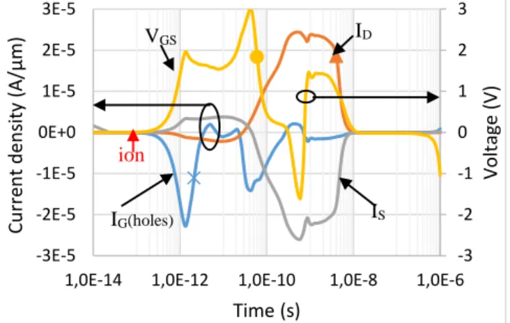
Fig 5 explain the mechanism of the transient current after the heavy ion strike. It shows that only the self-polarization of the gate by the holes current coming from ionized plasma leads to turn-on the device. The majority of the electron current coming from the source passes through the channel, reducing the electron current flowing through the GaN buffer or the whole structure to compensate for the accumulated holes, which minimizes the parasitic bipolar effect. This is confirmed again by Fig. 4 indicating that the transient current increases with the increase in the bias with same quantity of deposited charge.
-5,0E-6 0,0E+0 5,0E-6 1,0E-5 1,5E-5 2,0E-5 2,5E-5 3,0E-5 3,5E-5
1E-14 1E-12 1E-10 1E-08 1E-06
Drain cu rre n t d en sity (A/ µm ) Time (s) -3,00E-06 -2,50E-06 -2,00E-06 -1,50E-06 -1,00E-06 -5,00E-07 0,00E+00 5,00E-07 1,00E-06 1,50E-06 2,00E-06
1E-14 1E-13 1E-12 1E-11 1E-10
D rain c u rr en t (A/µm) Time -1E-5 0E+0 1E-5 2E-5 3E-5 4E-5 5E-5 6E-5 7E-5 8E-5 9E-5
1E-15 1E-13 1E-11 1E-09 1E-07
Drain curre n t d en sity (A/ µm ) Time (s) ion ion
Since the ionization coefficients are exponentially related to the electric field, rise of the polarization increases the generation of electron–hole pairs increasing the hole current in the gate, leading to more charge enhancement as though the saturation drain current was increased with the increase in gate bias (VGS)
in the on-state.
Fig. 5. Evolution of ID, IS,IG and VGS as a function of time following an
impact ionizing from the front side at VDS = 200 V in blocking state
We assume that the minor effect of the parasitic bipolar transistor in such devices induces that the triggering is always reversible and drain current can not be maintained, unlike the case of MOSFET devices, when the failure mechanism is linked to the avalanche and the forward biasing of the parasitic bipolar transistor, both providing charges to each other [8].
B. Proposal scenarios of Single Event Effect
The plasma generated by a heavy ion can occupy a large part of this small device inducing a big dE/dt which gives a big displacement current. This current may be recovered in the electrodes since the size of these components is very small. Results in Fig. 6 and 7 could provide possible scenarios of SEE in normally-off GaN power transistors under heavy ion. The displacement current, caused by the abrupt change of VDS or
VDG immediately after heavy ion impact, is shown in Fig. 6
without impact ionization model and in Fig. 7 with impact ionization model. Concerning the first case (without impact ionization model), the displacement current does not appear immediately after the ion impact: this current increases with the transient drop of VDS and decreases when VDS ascends. On the
other side, when the impact ionization model is considered, a very important displacement current (0.1 A/ µm), nearly 1000 times larger than the current observed without the impact ionization model. This current appears just after the ion impact at the same time VDS increases (see Fig. 7 zoom) and before the
drop voltage. Even if this displacement current caused by the avalanche phenomenon occurs during a very short time, we assume that this mechanism is probably the origin of SEE in these devices since usually the avalanche phenomenon in the real components is not reversible. This mechanism is observed only in the highest VDS over than 200 V. for VDS less than 200V
the impact ionization mechanism has no effect (Figure available in the final version). More arguments and details will be provided in the final paper.
Fig. 6. Evolution of deplacement drain current (IDD) and VDS as a function of
time following an impact ionizing from the front side at VDS = 400 V in blocking state (without impact ionization model)
Fig. 7. Evolution of deplacement drain current IDD and VDS as a function of
time following an impact ionizing from the front side at VDS = 400 V in blocking state (with impact ionization model)
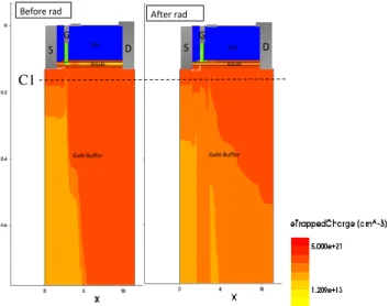
C. Effect of radiation on the electric field
The decrease of the electric field before and after the impact of heavy ion has been analyzed. Fig. 8 shows a systematic observation of the electric field in the simulated structures before and after heavy ion radiation at 100V. Results shows that the electric field significantly decreases along the structure after radiation. Fig. 7 indicates that the density of traps have a significant effect on the peak of the electric field observed after radiation. Since the detrapping is more important in the ions strike close to the gate electrode, the electric field will be more decreased in this area. This may explain the increase in breakdown voltage observed in [9]. In contrast, for RF normally-on HEMT, Erin et al. suggest that the density of traps does not have a significant effect on the peak of the electric field observed after radiation [10]. They explain that it could be due to post-radiation traps formed in the AlGaN/Nitride interface, not to post-radiation traps formed in the GaN-buffer layer; it is the same explanation that was adopted by Travis et al. [11] in their radiative tests (2 MeV protons) on AlGaN/GaN HEMT with different substrates (Si, SiC and Al2O3). This difference reveals
that the density of traps in the GaN buffer layer has a more significant effect in normally-off than in normally-on HEMTs.
-3 -2 -1 0 1 2 3 -3E-5 -2E-5 -1E-5 0E+0 1E-5 2E-5 3E-5
1,0E-14 1,0E-12 1,0E-10 1,0E-8 1,0E-6
Volt age (V) Curr en t d en sity (A/ µm ) Time (s) 0 50 100 150 200 250 300 350 400 450 -5,0E-05 1,0E-19 5,0E-05 1,0E-04 1,5E-04 2,0E-04 2,5E-04
1,0E-14 1,0E-12 1,0E-10 1,0E-8 1,0E-6
Drain v o lta ge (V) cu rre n t d en sity (A/ µm ) Time (s) 0 50 100 150 200 250 300 350 400 450 -0,01 0,01 0,03 0,05 0,07 0,09 0,11 0,13
1,0E-14 1,0E-12 1,0E-10 1,0E-8 1,0E-6
Drain v o lta ge (V) cu rre n t d en sity (A/ µm ) Time (s) 390 395 400 405 410 415 0,03 0,04 0,05 0,06 0,07 0,08 0,09 0,10 0,11 0,12
1,0E-14 1,0E-13 1,0E-12 1,0E-11 1,0E-10
Drain v olta ge (V) curre n t de n sity (A/ µm 2) Time (s) ID IS VGS IG(holes) VDS IDD VDS IDD ion ion ion
More results about the electrical and physical change after radiation will be provided in the final paper.
Fig. 8. Electric Field decrease (horizontal section at C1 of Fig. 9)
Fig. 9. Electron traps density before and after radiation
V. CONCLUSION
We explain the mechanism of the transient current after the heavy ion strike in normally-off GaN power transistors. The self-polarization of the gate by the holes current coming from ionized plasma leads to transient turn-on the device. We assume that the minor effect of the parasitic bipolar transistor in such devices induces that the triggering is always reversible and drain current can not be maintained. Possible mechanism of SEE in this devices under heavy ion has been proposed. a heavy ion can induce in these very small devices a huge displacement current (0.1 A/ µm) caused by the avalanche phenomenon in high voltage and the abrupt change of VDS or VDG immediately after
heavy ion impact is probably the origin of SEE in these devices. The density of traps have a significant effect on the peak of the electric field observed after radiation which may explain the increase in breakdown voltage observed in literature.
VI. REFERENCES
[1] Alexander et al. “Radiation effects in GaN materials and devices,” J. Mater. Chem. C, 2013, 1, 877–887 | 879.
[2] Sentaurus TCAD Tools, Synopsys, Inc., Mountview, CA, 2009.
[3] Datasheet of EPC2019,
http://epc-co.com/epc/Portals/0/epc/documents/datasheets/EPC2019_dat asheet.pdf.
[4] H. Dussault, J. W. Howard, Jr, R. C. Block, M. R. Pinto, W. J. Stapor, and A. R. Knudson, “Numerical simulation of heavy ion charge generation and collection dynamics,” IEEE Transactions on Nuclear Science, vol. 40, no. 6, pp. 1926–1934, December 1993.
[5] H. Dussault, J. W. Howard, Jr, R. C. Block, M. R. Pinto, W. J. Stapor, and A. R. Knudson, “The effects of ion track structure in simulating single event phenomena,” in Proc. 2nd Eur. Conf. RADECS, Sep. 13–16, 1993, pp. 509–516.
[6] D.McMorrow,A.R.Knudson, J.B.Boos, D. Park, and J. S. Melinger, “Ionization-Induced carrier transport in InAlAs/InGaAs high electron mobility transistors,” IEEE Transactions on Nuclear Science, vol. 51, no. 5, pp. 2857–2864, October 2004.
[7] D. McMorrow, J. S. Melinger, A. R. Knudson, S. Buchner, L. H. Tran, A. B. Campbell, and W. R. Curtice, “Charge-enhancement mechanisms of GaAs field-effect transistors: Experiment and simulation”, IEEE Transactions on Nuclear Science, vol. 45, no. 3, pp. 1494–1500, June 1998.
[8] M. Zerarka, P. Austin, and M. Bafleur, “Comparative study of sensitive volume and triggering criteria of SEB in 600 V planar and trench IGBTs”, Microelectron. Reliab., vol. 51, no. 9–11, pp. 1990–1994, Sep.–Nov. 2011
[9] S.J. Peartan, Ya-shi Hwang, F. Ren, “Radiation Effects in GaN-Based High Electron Mobility Transistors,” Springer US, JOM, volume 67, Issue 7 , pp 1601-1611, March 2015. [10] Erin et al., “Modeling Proton Irradiation in AlGaN/GaN HEMTs: Understanding the Increase of Critical Voltage,” IEEE Transactions on Nuclear Science, vol. 60, no. 6, pp. 4103 - 4108, December 2013.
[11] Travis J. Anderson et al., “Substrate-Dependent Effects on the Response of AlGaN/GaN HEMTs to 2-MeV Proton Irradiation,” IEEE Electron Device Letters, vol. 35, no. 8, August 2014. S D G SiN GaN-Buffer AlGaN Before rad G S SiN D GaN-Buffer AlGaN After rad C1 Before rad After rad 1 1.5e+061 1e+061 5e+05 1 Source1 FP1 Drain1 Ga te 1