HAL Id: tel-01629767
https://tel.archives-ouvertes.fr/tel-01629767
Submitted on 6 Nov 2017HAL is a multi-disciplinary open access
archive for the deposit and dissemination of sci-entific research documents, whether they are pub-lished or not. The documents may come from teaching and research institutions in France or abroad, or from public or private research centers.
L’archive ouverte pluridisciplinaire HAL, est destinée au dépôt et à la diffusion de documents scientifiques de niveau recherche, publiés ou non, émanant des établissements d’enseignement et de recherche français ou étrangers, des laboratoires publics ou privés.
Supramolecular self-assemblies for plasmonics : a
bottom-up approach to efficient photonic nanodevices
Sylvain Le Liepvre
To cite this version:
Sylvain Le Liepvre. Supramolecular self-assemblies for plasmonics : a bottom-up approach to efficient photonic nanodevices. Materials Science [cond-mat.mtrl-sci]. Université Paris Saclay (COmUE), 2017. English. �NNT : 2017SACLS330�. �tel-01629767�
Supramolecular self-assemblies
for plasmonics : a bottom-up
approach to efficient photonic
nanodevices
Thèse de doctorat de l'Université Paris-Saclaypréparée au CEA Saclay (SPEC) École doctorale n°572 Ondes et Matière (EDOM)
Spécialité de doctorat: Nanophysique
Thèse présentée et soutenue à Gif-sur-Yvette, le 26 septembre 2017, par
Sylvain Le Liepvre
Composition du Jury : Jean-Jacques Greffet
Professeur, IOGS Président
Nathalie Katsonis
Professeur Associé, University of Twente Rapporteur
Joël Bellessa
Professeur des Universités, Université Lyon 1 Rapporteur
Steven de Feyter
Professeur, KU Leuven Examinateur
Sylvain Barbay
Professeur, C2N Examinateur
Fabrice Charra
CEA, SPEC Directeur de thèse
N N T : 20 17 S A CL S 3 30
Remerciements 5
Introduction 9
1 Supramolecular self-assemblies and optical absorption 13
1.1 PTCDI on graphene . . . 15
1.1.1 Scanning tunneling microscopy. . . 15
1.1.2 PTCDI-C13 Transmission spectra. . . 16
1.2 Intermolecular interactions . . . 19
1.2.1 Non pertubative multipolar 2D model . . . 23
1.3 Graphene-molecule interactions . . . 24
1.3.1 Electromagnetic interactions . . . 24
1.3.2 Change of molecular conformation . . . 31
1.3.3 Electronic interactions . . . 31
1.4 Dependence on the intermolecular distance . . . 32
1.5 Dependence on the molecule-graphene distance . . . 37
1.6 PTCDI multilayer thin film . . . 41
1.7 Conclusion . . . 44
2 Supramolecular self-assemblies and fluorescence 47 2.1 Theoretical considerations . . . 49
2.1.1 Relaxation paths . . . 49
2.1.2 Energy transfer mechanisms . . . 50
2.2 Janus Tecton on graphene . . . 51
2.2.1 PTCDI-JT . . . 51
2.2.2 TBC8-JT . . . 58
2.3 Multilayers of Perylene derivatives . . . 59
2.4 Conclusion . . . 60
3 Vibrations of supramolecular self-assemblies on graphene 63 3.1 Introduction to Raman scattering . . . 65
3.2 Graphene Raman spectrum . . . 67
3.3 DFT computations . . . 70
3.4 Resonant self-assembled monolayer on graphene . . . 72
3.5 Non-resonant self-assembled monolayer on graphene . . . 75
3.6 Conclusion . . . 78
4 Plasmon engineering 79 4.1 Characteristics of plasmon modes . . . 81
4.1.1 Rabi frequency . . . 81
4.1.2 Field confinement and propagation length . . . 82
CONTENTS
4.2 Maxwell-Garnett materials . . . 83
4.2.1 Glass inclusions. . . 84
4.2.2 Absorber inclusions. . . 84
4.2.3 Gain medium inclusions. . . 85
4.3 Analysis of SPP dispersion relation . . . 88
4.3.1 Numerical dispersion relation. . . 88
4.3.2 Experimental dispersion relation . . . 90
4.4 High-Q plasmon modes . . . 92
4.5 Conclusion . . . 94
5 Strongly coupled self-assembled dyes and plasmons 95 5.1 Anti-crossing in self-assembled PTCDI on gold systems . . . 98
5.1.1 Tuning the Rabi frequency . . . 98
5.1.2 Experimental evidence of anti-crossing . . . 100
5.2 Luminescence of self-assembled PTCDI on gold . . . 100
5.2.1 Strong coupling and Stokes shift . . . 100
5.2.2 Experimental wavevector resolved luminescence spectra . . . 103
5.3 Conclusion . . . 104
6 Supramolecular self-assemblies for plasmon amplification 107 6.1 Molecular self-assemblies as gain medium . . . 109
6.1.1 Stimulated emission of plasmons . . . 109
6.1.2 Molecular self-assemblies as gain media . . . 110
6.2 Gain limitations in self-assembled thin films . . . 113
6.2.1 Yield, spectrum and decay dependence on pump power . . . 114
6.2.2 Time-resolved fluorescence spectra . . . 115
6.2.3 Electronic transition model . . . 116
6.3 Conclusion . . . 119
Summary 121 Synth`ese 123 A Dipole-field interactions theoretical calculations 125 A.1 Frequency to local electric field shifts relation demonstration . . . 125
A.2 Absorption of an oriented dipole monolayer . . . 127
A.2.1 Transverse electric polarization . . . 127
A.2.2 Transverse magnetic polarization . . . 128
B Self-assembled systems on graphene absorption spectra 131 B.1 Table of experimental shifts and broadenings . . . 131
B.2 Polymers on graphene . . . 132
B.3 Small molecules on graphene . . . 135
B.4 Annealing effects on absorption spectra . . . 138
B.5 Vibrational spectra . . . 139
B.5.1 PTCDI-C13 FTIR spectra . . . 139
B.5.2 Self-assembled TSB on graphene Raman spectra . . . 139
C Experimental methods 143 C.1 Materials . . . 143 C.1.1 Graphene . . . 143 C.1.2 Perylene derivatives . . . 143 C.2 Deposition techniques . . . 143 C.3 STM experiments . . . 144 C.4 Optical characterization . . . 144 C.4.1 Absorption spectra . . . 144
C.4.2 Fluorescence spectra and lifetimes . . . 144
C.4.3 Raman spectra . . . 144
C.5 Numerical computations . . . 144
C.5.1 Molecular structure . . . 144
C.5.2 DFT Calculations . . . 144
Apr`es ces trois ann´ees passionnantes pass´ees au Laboratoire d’Electronique et de Nanopho-tonique Organique (LEPO), j’aimerai remercier chaleureusement mon directeur de th`ese Fabrice Charra pour sa gentillesse, sa disponibilit´e, ses observations toujours tr`es perti-nentes, son aide en toutes circonstances et sa patience pour expliquer clairement les points les plus obscurs abord´es pendant ce travail de th`ese.
J’ai ´et´e marqu´e pendant cette p´eriode par le cadre tr`es sympathique du laboratoire et je voudrais remercier `a ce titre tous les membres permanents de l’´equipe qui cr´eent cet environnement de travail si agr´eable, autant du point de vue humain que scientifique : C´eline Fiorini, Ludovic Douillard, Simon Vassant, Bruno Delomez.
Cette exp´erience n’aurait pas ´et´e la mˆeme sans les bons moments pass´es avec les non-permanents de l’´equipe : Maud Jaouen pour ses conseils en d´emontage de STM, Patrick Hsia et sa science cin´ematographique, C´eline Molinaro et les frites bruxelloises, Sarra Mitiche et les fleurets anciens, Farid Kameche et ses th´eories sur les kebabs, Mohammed Houssat alias Barack Obama, L´ea Constans, Alice Six, Morgan Auffray, Ana¨ıs Gouesmel, Kim Nguyen, Tessnim Sghaier, Yasmine Nahas, Nathalya Kalashnyk, Quanbo Jiang, Mar-tin Melgarejo, Bastien Jouy, S´ebastien Jean-Louis, Milino Kerowgodage et Paul Bouteyre.
Je tiens `a remercier l’´equipe du C2N qui m’a accueilli pour quelques semaines d’exp´eriences au sein de leur laboratoire, et avec qui il a ´et´e tr`es agr´eable de collaborer tout au long de cette th`ese: Sylvain Barbay, Alejandro Giacomotti, John Bigeon, Ariel Levenson.
Merci `a toutes les personnes ayant collabor´e aux diff´erents projets de cette th`ese, beaucoup de belles discussions scientifiques ou plus g´en´erales ont r´esult´e de ces rencontres. Merci `a toute l’´equipe de l’UPMC : Andr´e-Jean Attias, Fabrice Mathevet, David Kreher, Lydia Sosa-Vargas, `a Philippe Lang de Jussieu, `a Ludovic Tortech, Quentin Arnoux, Sylvie Marguet, Vincent Derycke, Thomas Gustavsson et Valentin Maff´eis du CEA Saclay ainsi que Jean-Paul Hugonin de l’IOGS.
Tout ce travail n’aurait pu voir le jour sans le soutien de mes proches. Pour ´eviter le cˆot´e un peu lourd de l’exercice des remerciements, je ne peux m’empˆecher de citer le golfeur Greg Norman excellant dans ce registre : ”Je dois beaucoup `a mes parents, surtout `
a ma m`ere et `a mon p`ere”. Bref merci papa merci maman et merci les fr´erots d’avoir appris plein de trucs au petit dernier.
Dans la cat´egorie abn´egation, je dois une mention sp´eciale remerciement `a ma femme Elise qui a fait et qui fait toujours l’effort de comprendre des parties de plus en plus vaste de ce travail de th`ese, mˆeme si les liens avec l’´electrom´enager r´enov´e garanti restent quand mˆeme assez t´enus.
Toujours grands seigneurs en termes de conseils avis´es, constructeurs de l’extrˆeme, aventuriers sans peurs et sans reproches, mais par-dessus-tout, colocs, j’aimerai claquer un tchek reconnaissant aux colocs de l’Hay Simon, Hadrien et Guillaume, et par extension `
a toute la famille de la d´egaine. (Division d’Escalade Giffoise A´erienne Innovante Nova-trice et Engag´ee). Mention sp´eciale `a Goulven pour son caramel. (le plus goutˆu de tout landerneau !)
J’allume `a cette ligne la flamme du copain non cit´e dans les remerciements, tragique sort pour celui qui a tant œuvr´e pour me soutenir, me distraire, m’essouffler au cours
REMERCIEMENTS
de cette th`ese, h´eros de l’ombre `a qui les portes de l’immortalit´e du papier viennent de se fermer subitement. Puisse cette flamme porter ton ˆame en souvenir aux g´en´erations futures.
Sur ce, bouclez vos ceintures, rep´erez les issues de secours (qui peuvent se situer derri`ere vous !), PNC aux portes, on va d´ecoller !
- Oscar Wilde
”There’s plenty of room at the bottom”. Here are the words of Richard Feynman at an American Physical Society meeting at Caltech in 1959, describing its vision of a technology working at the ultimate atom scale. This landmark can be considered as the beginning of the nanotechnology field which is devoted to the study and the manufacture of structures ranging in size from 1 to 1000 nm. The development of powerful tools such as the scanning tunneling microscope (STM),1 the atomic force microscope (AFM)2 and other scanning
probe microscopes3 in the 80s have fostered research at the nanoscale giving means to observe and manipulate systems as small as individual atoms.4
Furthermore, the discovery of low-dimensional materials such as fullerene,5 carbon nanotubes,6,7graphene,8 single layer boron nitride9has revealed the potential of nanotech-nology for a vast number of fields such as energy (solar cells,10 fuel cells,11 batteries12),
information and communications (transistors,13 transparent conducting electrodes,14
op-toelectronics15), medicine (tissue engineering,16 bioimaging,17 drug delivery18), environ-ment (contamination removal,19 pressure sensors,20 molecular sensor21). However, the nanotechnology era is just beginning and important progresses have to be made aiming at the design of matter at the nanoscale and at the development of practical applications in most of the fields mentioned above.
Two strategies can be mentioned when trying to miniaturize existing systems. The top-down approach pushes the limits of existing tools such as UV lithography or etching techniques to form smaller systems. This strategy is for example used by the semiconductor industry to scale the size of transistors down to ∼ 10 nm today.22
On the other side, the bottom-up approach is an additive technology using small build-ing blocks such as molecules or atoms to create complex nanoscale systems. Supramolec-ular self-assembly is one of the most advanced techniques able to generate periodically-replicated well-ordered molecular architectures with well-controlled geometry. By chemi-cal design of molecular building blocks, their molecular recognition abilities can be finely tuned so as to spontaneously arrange themselves, forming pre-programmed 1D, 2D or 3D supramolecular architectures.23,24,25
Various molecular-recognition processes are at the origin of the self-assembly architec-ture, from steric hindrance26 to hydrogen bonding,27 metal coordination28 or
interdigita-tion of alkyl chains.29,30,31
The fabrication of such systems is simple and does not require complex tools unlike top-down approaches. The formation of molecular self-assemblies can easily be obtained by drop casting or by dip coating techniques, which essentially consists in evaporating a solution containing the molecular building blocks on a targeted substrate. The self-assembly processes can also take place with molecules deposited in ultra-high vacuum environments using molecular beam epitaxy techniques to gain control over the formation of the supramolecular self-assembly.
Plasmonics exploits collective oscillation of electrons in metallic structures to confine optical fields on dimensions much below their wavelength. This offers unique opportuni-ties for subwavelength optical waveguiding and enhancements of light-matter interactions through intense local fields and optical antennas.32 Nanoplasmonics has made major
INTRODUCTION
advances thanks to recent developments in nanoscale manufacturing techniques. The possible applications of this field in full development cover wide segments of technology: spectroscopy,33nanophotonics,34,35 biological sensors,36,37 imaging,38 cancer treatment.39 In recent years, the physics and applications of plasmonic waves interacting with quan-tum emitters became a hot topic.40 In particular, the coupling between a highly confined
plasmonic waveguide and an optical gain medium attracted much attention since the prospect of overcoming propagation losses paves the ways to the development of pho-tonic integrated circuits with subwavelength scale working at optical frequencies.41
Fur-thermore, a robust active plasmonics device would find applications in the realization of photovoltaic cells and light-emitting diodes,42 biomedical sensors, fluorescent labels and light-triggered actuators.43
Various gain media have been used to demonstrate Surface Plasmon Amplification by Stimulated Emission of Radiation (SPASER) such as semiconductors44 or π-conjugated molecules dispersed in a polymer matrix.45
It has been shown that the distance and the orientation between the fluorophores and the metal surface plays a crucial role on the coupling between the gain medium and the plasmon mode.46 At small distances, Dexter electron exchange quenching of emitter flu-orescence is preponderant and overcompensates plasmonic enhancements. Moreover, the plasmon mode electric field is mainly perpendicular to the metal surface and thus inter-acts more strongly with emitters displaying the same orientation. Therefore, a gain of control over the hybrid plasmonic-emitter system structure, especially in the positioning of the emitter relatively to the metal surface could lead to a neat increase of the efficiency of such active plasmonics devices. Finally, the important spatial confinement of the plas-monic mode electromagnetic field requires a high density of photoactive species in the gain medium to increase the number of emitter interacting with the electromagnetic mode.
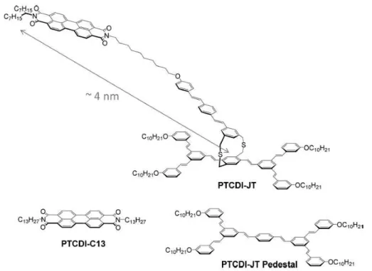
Supramolecular self-assembly offers the flexibility to finely tune molecular scale po-sitioning on a targeted substrate through the chemical design of the molecular building blocks. the concept of Janus-like 3D molecular tectons introduced few years ago47could be
used to reduce the Dexter quenching of self-assembled π-conjugated molecules on a metal-lic surface. In these systems, molecular building blocks display a dual-functionalization at two opposite faces linked by a rigid insulating spacer: a pedestal manages the 2D self-assembly on the substrate whereas a dye group provides the photonic functionality. Therefore, the lateral organization of the self-assembly array is maintained while lifting photoactive entities by a few angstr¨oms above the substrate surface thanks to the spacer group. Such Janus tecton approach paves the way for the precise distance and orientation positioning of a photoactive entity with reference to a substrate surface, potentially a plas-monic waveguiding surface. Furthermore, very high molecular volume or areal densities can be reached in supramolecular self-assemblies. Such hybrid systems would significantly increase the number of emitters interacting with a confined plasmonic mode.
However, the aggregation of dyes strongly affects their photonics properties. Inter-molecular interactions lead to increasing or decreasing radiative recombination rates as well as frequency shifts in the absorption and fluorescence spectrum, depending on con-structive or decon-structive intermolecular interactions. Experimental and theoretical work have to be done to determine how do supramolecular self-assemblies tune the photonics properties of an active layer through the precise design of intermolecular orientation and positioning.
In this work, we study the photonic properties of self-assembled molecular monolayers on graphene by correlating the self-assembly structure as deduced from scanning tunneling and atomic force microscopies to photonic properties as analyzed by optical spectroscopy measurements. We demonstrate the strong-coupling regime between a 3D molecular self-assembly and a propagating plasmon polariton mode, and show that the optical gain in
such dense optically active systems saturates at high excitation rate.
• In chapter 1, we study the optical absorption of perylene derivative self-assembled monolayers on graphene and explore the effect of intermolecular and molecule-graphene interaction on the absorption spectrum of such hybrid systems. An ex-ample of a three-dimensional perylene self-assembly optimized for interacting with propagating plasmon polariton is also demonstrated.
• Chapter 2 deals with fluorescence of molecular self-assemblies on graphene. The first fluorescent non-covalent functionalization of graphene by a supramolecular self-assembled monolayer is demonstrated using a Janus tecton approach. The fluores-cence signals of three-dimensional supramolecular self-assemblies suitable for inter-acting with propagating plasmon polaritons are studied.
• Vibrational properties of self-assembled monolayers on graphene are explored in chapter 3. We show the appearance of a coupled vibrational mode between adsorbed molecules and graphene.
• In chapter 4, we study how to engineer plasmonic modes to reduce losses in the metal. We demonstrate an approach to design plasmonics resonators with high quality factors.
• Strong-coupling between a three-dimensional self-assembly and a propagating plas-mon polariton mode is deplas-monstrated in chapter 5. The photonics properties of such a system are studied through its absorption and emission responses.
• Finally, chapter 6 presents the conditions for amplifying plasmonic systems by com-paring traditional gain media to molecular self-assemblies. The gain limitation of molecular self-assembly systems is studied, and important losses due to exciton-exciton recombination are evidenced.
These chapters relate research projects carried out in collaboration with other teams without whom this work would not have been possible. Andr´e-Jean Attias group (UPMC) worked on designing and synthetizing spontaneously assembling molecules at the graphene surface (chapters 1 and 2), Matthew Williams and David Andrews (Univ. East Anglia) performed DFT calculations to compute Raman spectra in chapter 3, John Bigeon and Sylvain Barbay (C2N) carried out numerical calculations and experimental characterizations of the plasmonic systems in chapter 5, Valentin Maff´eis and Thomas Gustavssonn performed time resolved fluorescent spectra on PTCDI thin films in chapter 6, Philippe Lang (ITODYS) performed IR experiments (Appendix B), Yannick Dappe (CEA/SPEC) performed DFT calculations to com-pute the density of states (DOS) of adsorbed molecules on graphene (Appendix B), Ludovic Tortech (CEA/NIMBE) was of a precious help for the realization of self-assembled thin films by its advice and the lending of its equipment (chapters 1-3 ,5 and 6).
Supramolecular self-assemblies
and optical absorption
Supramolecular self-assemblies on highly ordered pyrolitic graphite (HOPG) probed by a scanning tunneling microscope (STM). The presence of molecules is indicated by the yellow color in the STM image. Self-assembled molecules: TBC8 (top left, 11 nm x 11
nm), TBC8-JT (bottom left, 100 nm x 100 nm), P3HT (top right, 65 nm x 65 nm), PTCDI-2C6a (bottom right, 45 nm x 45 nm).
Exotic molecular network patterns such as those displayed above can be drawn on various surfaces by designing carefully the structure of molecules that will form the self-assembly. When this system consists of self-assembled dye molecules, what color does it have? Would it be possible to engineer the color of self-assemblies by changing the geometrical parameters of the 2D molecular network?
1. SUPRAMOLECULAR SELF-ASSEMBLIES AND OPTICAL ABSORPTION
Close-packed assemblies of dye molecules exhibit drastically altered photonic properties as compared with the isolated or diluted species.48 These changes find their origin in
near-field optical interactions between the constituent molecules, as early predicted by McRay and Kasha.49 A well-known example is the spectral shift induced by the self-association of cyanine dyes in solution.50 Depending on the aggregation pattern of the dyes,
either bathochromically shifted J-bands or hypsochromically shifted H-bands are formed, corresponding to collectively excited states and energy bands of delocalized excitons.51,52 The giant transition dipole moments associated with such excitations result in en-hanced optical interactions, e.g., with plasmon resonators in which case a strong-coupling regime can then be reached.53,54 These collective excitations can also lead to remarkable light emission processes such as superradiance.55
Interactions between a dye and its surroundings at the molecular scale may also induce drastic changes in its photonic properties. Structural planarization of the ad-sorbed molecules,56 or the immersion inside a polarizable medium57 can induce uniform
bathochromic shifts of the vibronic bands constituting the absorption spectrum.
Finally, when distances between π-conjugated systems are small enough to permit electron tunneling, quantum effects can also come into the play, at the origin, for instance, of new intermolecular charge-transfer absorption bands.58,59
Consequently, the fine tuning of molecular-scale organization of condensed dye assem-blies appears critical for the control of photonic properties of matter and possibly for the generation of original photonic processes.
An atomically precise positioning of self-associated molecular dyes can be achieved either in vacuum or at the solution–substrate interface by self-assembly techniques.
A high level of control of the self-assembly geometry is possible by exploiting the interactions between alkyl side chains and the surface of highly oriented pyrolytic graphite (HOPG),60 beyond H-bond-steered organizations.61 Based on these principles, it has been possible to design molecular building blocks that arrange spontaneously according to various predetermined patterns.31
Graphene has focused intensive research in the past 10 years due to its unusually high electron mobility, atomic thickness, broadband optical absorption, and unique flex-ibility.62,63,64,8 CVD-grown graphene, being easily transferable onto arbitrary substrates
while preserving high electronic mobilities,65soon appeared as a tantalizing candidate for various applications in photonics,15such as solar cells,66high-speed photodetectors,67light sources,68ultrafast lasers,69and metamaterials.70 However, as a zero-band-gap semimetal,
pristine graphene has a narrow range of roles, merely limited to transparent electrodes. Advanced applications require graphene to be synergistically combined with nanomaterials providing complementary properties.
Recently, noncovalent functionalization of graphene with organic molecular building blocks has appeared as a promising way to modulate its properties in view of functional applications. Actually, graphene provides an atomic-scale crystallographic lattice acting as a template guiding supramolecular self-assembly.71 This bottom-up elaboration process,
which implies the physisorption onto graphene of mostly planar molecules (tectons), is now well mastered in view of electronic applications. For example, supramolecular self-assembly on chemical vapor deposition (CVD)-grown graphene was used to dope graphene, and back-gated graphene field-effect transistor (G-FET) devices were obtained.72
Surprisingly, by comparison with electronics, the noncovalent functionalization of graphene is still in its infancy as concerns applications in photonics. Yet, organic dyes offer a high flexibility in the design of innovative photonic devices. Actually, because of their high oscillator strengths, they can play the role of light harvesters, photon sources, exciton fun-nels, etc., and as such should provide opportunities to enhance or extend the properties of graphene toward light-based applications.
Molecular self-assembly techniques on HOPG substrates can be extended to mono-layer CVD graphene as a substrate,73 which offers optical transparency when transferred
from its native CVD substrate usually copper– onto a transparent one such as quartz or polyethylene terephthalate (PET). This offers opportunities for advanced optical charac-terizations in a transmission geometry, such as polarized variable-incidence transmission spectroscopy. In addition, the electrical conductivity of a CVD graphene monolayer is sufficiently high to apply scanning tunneling microscopy (STM) and thus determine the structural data of the molecular assembly with atomic-scale accuracy.
Self-assembly of adsorbed conjugated molecules can influence the electronic properties of its substrate. Such a non covalent functionalization is especially suitable in the case of graphene because of its “surface only” nature74,75 and has been applied to tailor its band structure76 or its work function77,78 with a monolayer of PTCDI and similar molecules,
which can be laterally patterned79 or even manipulated at the single-molecule level.80 Through the combination of optical characterizations and structural control of dye assemblies on CVD graphene, detailed studies about the influence of the dye organization on photonic properties become feasible.
In the following, we explore how the optical absorption spectrum of a dye can be changed once self-assembled on a surface or on a three dimensional network.
1.1
PTCDI on graphene
Perylene-3,4,9,10 tetracarboxylic-3,4,9,10-diimide (PTCDI) and its sibling molecule perylene-3,4,9,10-tetracarboxylic dianhydride (PTCDA) have become archetypes for photonic ap-plications of dyes,81 for self-organized adsorption on various atomically flat surfaces,82 and for their combination. Indeed, optical differential reflectance spectroscopy,83
photo-luminescence, or Raman diffraction studies have evidenced optical responses attributed to strong interactions of PTCDA with metal84,85 or semiconductor86 substrates and be-tween neighboring molecules when deposited on a dielectric substrate87,88 or in multilayer structures.89 The optical effects of interactions between close-packed PTCDA molecules
deposited on epitaxial graphene have also been observed.90
1.1.1 Scanning tunneling microscopy.
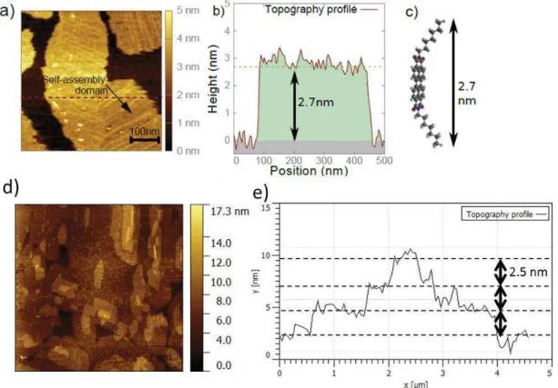
The self-assembly was probed on two graphitic substrates, highly oriented pyrolytic graphite (HOPG) and monolayers of CVD graphene transferred either onto fused silica (“optical quartz”) or PET. The resolution of carbon atoms is easily obtained on both systems. On CVD graphene samples, an additional moderate roughness is observed, which is attributed to the substrate (Figure 1.1). For example, in the case of graphene transferred onto a fused silica plate, this roughness attains 0.5 nm over distances of approximately 50 nm (Figure 1.1).
The PTCDI molecule has become a paradigm both as a self-assembly tecton and as a dye. For the present study, we chose an alkylated form of this dye, N, N ′−ditridecylperylene− 3, 4, 9, 10 − tetracarboxylicdiimide (PTCDI-C13), forming a spontaneously self-assembled monolayer at the interface between the solution and graphene. The monolayer structures have been studied by STM at the solution–substrate interface.
Figure 1.2 displays STM images of PTCDI-C13 monolayers on HOPG, on as-grown CVD graphene monolayer on copper foil and CVD graphene monolayer transferred onto PET. The STM technique favors the signature of aromatic skeletons which present higher electronic surface density of states close to the Fermi level.91
Intramolecular resolution is possible both with HOPG and graphene as substrates (Figure 1.2).
1. SUPRAMOLECULAR SELF-ASSEMBLIES AND OPTICAL ABSORPTION
Figure 1.1: Structural characterization of the substrates. STM images (2.3 × 2.3nm2) of a HOPG surface (a) and CVD monolayer graphene transferred onto a fused quartz plate (b: 2.3 × 2.3nm2 and c: 50 × 50nm2). The images were acquired under air atmosphere, in the height (constant current) mode. The setpoint current was IS = 100pA, and the bias
was VT = 200mV . The height scale is also shown for graphene on quartz (c).
Figure 1.2: Structural characterization of the self-assembled PTCDI monolayers. Molec-ular formula of PTCDI-C13 and STM images of self-assembled monolayers on HOPG (a: 14 × 14nm2) as-grown CVD monolayer graphene on copper foil (b: 11 × 11nm2) and CVD graphene monolayer transferred onto a PET plate (c: 8 × 8nm2). The typical current
setpoint and sample bias were 10 pA and 800 mV, respectively. The images were acquired at the interface between the substrate and a ca. 10−5M solution in phenyloctane at room temperature.
As expected from the atomically flat surface of HOPG, this substrate produces the largest domains. It permits an accurate determination of the lattice parameters, which correspond to a surface density of 0.45 molecules per nm2 and a distance between closest neighbors of ca. 1.4 nm. The network obtained on CVD graphene is compatible with that obtained on HOPG, with one molecule per unit cell. The various domains have a finite number of lattice orientations, indicating an epitaxial relationship with the graphitic lattice. These results are fully consistent with the expected formation of a self-assembled monolayer in which the molecules are lying flat on the substrate, with n-alkyl chains standing away from the graphene surface due to steric constrains of oxygen atoms.92
By randomly inspecting various regions of drop-cast samples, it appears that a nearly complete coverage (about 80%–90%) is obtained whereas the droplet spread on the sample contained the exact quantity of molecules needed to form a monolayer. The formation of a second layer is avoided by the presence of alkyl chains standing away from the surface that act as a buffer layer.
1.1.2 PTCDI-C13 Transmission spectra.
The solution spectrum of PTCDI-C13 is reported in Figure 1.3 (labelled “SOL”). It presents a typical vibronic signature of a π–π∗ transition. Vibronic transitions,
involv-Figure 1.3: Normal incidence transmission spectra T, expressed as an optical density DO = −log(T
T0). SOL: a 10−6M solution of PTCDI in toluene, cell thickness: 2 mm
(black curve). SAM1 and SAM2: two self-organized PTCDI-C13 monolayers on graphite, formed following two methods: drop casting (light blue, SAM1) or dip coating (dark blue, SAM2). µC: 10 equivalent monolayers of PTCDI-C13 deposited by solvent evaporation on a fused-quartz substrate, that is without CVD graphene (green curve) and PTCDI-C13 microcrystalline thin film (dotted green curve) reproduced after Mizuguchi et al.96 and rescaled for easier comparison. GR: monolayer CVD graphene transferred onto a fused-quartz plate (orange curve). All spectra are referenced (T0) to their corresponding naked substrate (GR for SAM1 and SAM2, quartz plate for µC and GR) or pure solvent (SOL). The energies of the 0-0, 0-1 and 0-2 vibronic bands are indicated for solution and monolayer spectra.
ing a change in both electronic and vibrational energy, can here be understood in the Franck-Condon approximation: electronic transitions are most likely to occur without changes in the positions of the nuclei in the molecular entity and its environment. As a consequence, the intensity of a vibronic transition is proportional to the square of the overlap integral between the vibrational wavefunctions of the two states that are involved in the transition.93 Bands in the absorption spectrum are then attributed to electronic vertical transitions from the ground vibrational state of the PTCDI-C13 highest occupied molecular orbital (HOMO) to the 0, 1 and 2 vibrational states of the lowest unoccupied molecular orbital (LUMO). The observed 0.18 eV (1450 cm−1) energy difference between 0-0, 0-1 and 0-2 sub-bands is characteristic from π-conjugated systems as present in the PTCDI core where p orbitals of neighbor carbon atoms overlaps.94
The main band is the 0–0 at 2.35 eV and corresponds to an absorption cross section σSOL = 3.3 × 10⁻¹⁶ cm2 consistent with the molar attenuation coefficient reported in
the literature for alkylated PTCDI.95 Quantum chemical calculations have shown that the transition dipole moment corresponding to the π–π∗ transition is aligned along the N –N′-axis.94
1. SUPRAMOLECULAR SELF-ASSEMBLIES AND OPTICAL ABSORPTION
The difference transmission spectra between self-assembled monolayer on a substrate of monolayer CVD graphene transferred onto fused quartz are shown in Figure 1.3. Two types of depositions are reported: (i) drop casting of a droplet of a toluene solution containing the exact amount of molecules needed for a coverage of 0.45 molecule per nm2 (SAM 1) and (ii) dipcoating in a ca. 10−5M solution in toluene followed by rinsing in
toluene and ethanol (SAM 2).
The transmission spectra of SAM1 and SAM2 are nearly identical and correspond to a bathochromic shift of 0.14 eV (1130 cm−1) of the whole vibronic system. This quantitative similarity further supports the homogeneous formation of one monolayer by dip coating, as was shown in the case of drop casting. At the maximum of the 0-0 absorption band, shifted to 2.21 eV, the relative transmission ∆TT is ca. 2.1% (SAM1) and ca. 1.9% (SAM2). For an absorbing monolayer deposited on a lossless dielectric substrate, the relative transmission depends only on the absorptive part of the molecular optical response.97 Given the molecule surface density of 0.45 molecule per nm2 measured by STM, the
molecular absorption cross section can be thus evaluated to σM L = 4.5 × 10⁻¹⁶ cm2.
By assuming an in-plane orientation of the N –N′-axis, which gives a factor of 3/2 cor-responding to a 2D orientational averaging of the transition dipole moments instead of the 3D averaging in solution, the above value is fully consistent with that obtained in solution (3.3 × 10⁻¹⁶cm2). Notice that accounting for the Lorentz local field correction to σSOL, [n
2 +1
3 2 1n with n being the index of refraction of toluene, and for the substrate-index
correction to σM L, n+12 with n being the index of the substrate,97 does not change this
conclusion (ca. 1.33 and ca. 1.25, respectively).
Microspectroscopy sampling of the sample, averaged over a spot of about 3µm in di-ameter have shown a high homogeneity of the absorption in the range of millimeters. Remarkably, in the absence of graphene coverage on the fused quartz substrate prior to PTCDI-C13 deposition, completely different transmission spectra are observed. Actu-ally, no measurable absorption is recorded after using the dip coating technique and the spectrum observed for drop casting is very similar to the one reported in the literature for PTCDI microcrystalline films96(µC, solid and dotted lines). Moreover, microspectroscopy
has shown a high inhomogeneity of the absorption strength, whereas the measured spectra acquired at different places remain homothetic.
Finally, we have measured the dependence on the incidence angle of the PTCDI ab-sorption spectral feature in the polarized abab-sorption for SAM1 and SAM2 samples (Figure 1.4). Whereas the absorption increases with incidence for TE polarization (blue triangles in Figure 1.4), it decreases monotonically with increasing incidence for TM polariza-tion (red squares). In both cases, the molecule spectrum changes homothetically, that is preserving the balance between vibronic bands. These observations confirm that the orientations of the transition dipole moments of the molecule are parallel to the substrate surface (graphene layer), as shown by the theoretical model98(continuous lines). This can be easily seen at grazing incidence where the TM polarized incident electric field is almost perpendicular to the surface, and therefore can’t be absorbed by optical dipoles parallel to the surface. This effect is even visible to the naked eye looking through a tilted plate through a polarizer. Notice that, for a thin film with random 3D molecule orientation, both TE and TM polarizations should exhibit an increased absorption at grazing incidence because the number of molecules illuminated by the incident beam increases.
The quantitative spectral analysis shows that the characteristic optical absorptions of drop-cast (SAM1) and dip-coated (SAM2) samples result from a homogeneous assembly of flat lying molecules with a surface density equivalent to one monolayer. Together with STM observations, this permits to unambiguously assign the spectral features observed at 2.21, 2.35 and 2.57 eV to the absorption of the PTCDI-C13 monolayer self-assembled onto the graphene substrate with a planar geometry of the molecules.
Figure 1.4: Optical signature of orientations of self-organized PTCDI-C13. Variable-incidence polarized-transmission analysis of the contribution of the self-assembled molecu-lar monolayer to the absorption (blue triangle: TE, red squares: TM). The optical density at the absorption maximum (λ = 561nm), as obtained from a fit of the absorption line of the molecule, is plotted. The continuous lines represent the TE and TM theoreti-cal absorption variations98 considering molecular transition dipole moments lying flat on graphene. For randomly oriented transition dipole moments, both TE and TM should increase with incidence following the blue line.
The most striking feature of the self-assembled monolayer spectra is the uniform red-shift of the whole vibronic spectral line, which results from the self-assembly. This red-shift is not accompanied by an important blurring of the spectral structures, consistent with the high homogeneity of molecular organization and environments obtained through the atomically precise self-assembly process on graphene. The energy difference between 0–0, 0–1 and 0–2 sub-bands is preserved, at 0.18 eV. This value is characteristic of the π-conjugated C–C double bond vibration and shows that the absorption remains dominated by the π–π∗ transition.
2D ordered aggregation of similar molecules on metals have been reported to induced drastic changes in optical spectra, attributed to new electronic transitions.85 Less
pro-nounced rigid spectral shifts have been reported previously for molecules deposited on crystalline dielectrics such as hexagonal boron nitride (h-BN).56,88 The cited possible ori-gins of such shifts are optical interactions between molecules or between molecules and the substrate and the deformation of molecules induced by van der Waals interactions between molecules and substrate.
1.2
Intermolecular interactions
Intermolecular optical interactions are a consequence of the local electric field resulting from the induced dipoles of molecules at neighboring sites.99 The Coulomb interaction between close molecules can result in the creation of a Frenkel exciton, a bound electron-hole pair whose electron-hole is localized at the molecule position.
Intermolecular distances in self-assembled systems are typically on the order of a nanometer. Thus, the retarded field can be neglected in the following and all calcula-tions are performed in the quasi-static regime.
1. SUPRAMOLECULAR SELF-ASSEMBLIES AND OPTICAL ABSORPTION The field emitted by a dipole d at a distance r(r, θ) is:
E(r, θ) = 1
4πǫr3(3(d.u)u − d) (1.1)
The dipole moment µ for a molecule at a certain frequency ω is related to the excitation local electric field through the polarizability α.
µ(ω) = α(ω)Eloc(ω) (1.2)
Since the incident electric field drives the molecular oscillator, all dipole moments in a molecular assembly are coherent in presence of an excitation field, in contrast to the case where molecules fluoresce.
In the following, molecules are considered identical and unidimensional. Therefore, the polarizability tensor has only one coefficient. It is possible to model in a classical picture (not quantum) the polarizability of the lone molecule applying Newton’s law to the electron cloud of mass m and charge q represented by its barycenter at position x:
md
2x
dt2 = FElocal+ Ftension+ Fdamping (1.3)
The first term represents the Coulombic interaction with the incident electric field, the sec-ond term represents the Coulomb force between the electron cloud and the molecule nuclei (spring force or Hooke’s law) that builds the electronic resonance, the third term repre-sents oscillator losses from which results the quality factor of the resonance. Considering a sinewave excitation at frequency ω, the above expression can be rewritten:
−ω2mx = qElocal− k(x − x0) + iγ0ωx (1.4)
Multiplying the two parts of equation 1.4 by the charge q, dividing by the mass m and replacing the dipole moment by its expression µ = qx, we can write:
−ω2µ + ω0µ − iγωµ =
q2E local
m (1.5)
The theoretical expression of the polarizability can then be written: α(ω) = q
2/m
ω2
0− ω2− iγω
(1.6) At resonance, the real part of the polarizability is zero. The imaginary part of the polarizability can be evaluated through the absorption cross-section σ from:
σ = Im(α0)ω0 3ǫ0c
(1.7) It is experimentally determined by a molar absorptivity ǫ (L × mol−1× cm−1) mea-surement through:
σ = 1000ln(10) ǫ
NA = ǫ × 3.82 × 10
−21 cm2 (1.8)
Where NA is the Avogadro number, ω0 is the resonant frequency, and c the speed of
light.
We plot in figure 1.5 the electric field emitted by a perylene dye as a function of the distance from this dye in vacuum (n = 1). We use the PTCDI molar absorptivity to compute the polarizability (ǫ = 87000 Lmol−1cm−1). We compare these values to the incident electric field of a linearly polarized plane wave created by a continuous-wave (CW) laser at the PTCDI resonance wavelength (530 nm). In microscopy experiments, it
Figure 1.5: Electric field emitted by a perylene dye (blue curve) in the quasi-static limit and electric field of a plane wave created by a laser beam (10 µW.µm−2) (red curve)
is common to focus a 10 µW beam onto a 1 µm2 surface. The typical irradiance (energy flux) of such plane wave can be written as:
I = nǫ0c 2 E
2 (1.9)
Far from the dipole, the field emitted by the dipole is negligible in comparison to the exciting laser field. Close to the dipole, the dipole field becomes predominant. The characteristic length delimiting these two regime is a few nanometers, as shown in figure 1.5. This characteristic length does not depend on the amplitude of the incident electric field since the field emitted by the dye at a certain distance is proportional to the incident electric field.
The local electric field is the sum of the incident electric field and the field re-emitted from the molecules, i.e. the field experienced by a given molecule in the assembly. We introduce a geometrical parameter k which accounts for the distance and the orientation between neighboring dipoles.
Eloc(ω) = Einc(ω) + kµ(ω) (1.10)
The combination of equations 1.2 and 1.10 gives a new expression for the dipole moment of the molecule as function as the incident electric field rather than the local one.
µ(ω) = α(ω)
1 − kα(ω)Einc(ω) (1.11) One can then introduce from equation 1.11 an effective polarizability αp(ω) :
αp(ω) =
α(ω)
1 − kα(ω) (1.12) To get insight about the effective polarizability, we consider two identical molecules with parallel dipole moment spaced by a distance r and with an angle θ between the dipole moment axis of one molecule and the line joining the two molecules. The k geometrical factor is:
k = 1
4πεr3(3cos
2(θ) − 1) (1.13)
The k factor can be positive if θ = 0 (dipoles are aligned) or negative if θ = π2 (dipoles are parallel, sideways).
1. SUPRAMOLECULAR SELF-ASSEMBLIES AND OPTICAL ABSORPTION
Using the expression of the polarizability developed in equation 1.6, the effective polarizability can be rewritten as:
αp(ω) = q2/m ω2 0 − kq2 m − ω2− iγω (1.14) Figure 1.6 displays the k geometrical factor in SI units computed for several geometries of interacting PTCDI and associated imaginary part of the effective polarizability deduced from the geometrical factor k and a fit to the polarizability of isolated PTCDI diluted in a toluene solution as described in equation 1.14.
Figure 1.6: Top. Interacting dipoles geometry and associated geometrical factor k in SI units. To model the PTCDI network on graphene, d = 1.5 nm and θ = 45◦.92 Bottom. Imaginary part of the polarizability for isolated PTCDI when diluted in a toluene solution (black, fit to the experimental data), computed effective polarizabilities for geometrical parameters (SI units) : 1.9 × 1036 (blue), −9.4 × 1035 (red), 5.3 × 1036 (cyan), 1.2 × 1037 (green).
A negative k constant (alongside parallel dipole configuration) produces a blue shift and a lowering of the peak absorption. A positive k constant (aligned dipoles configu-ration or PTCDI 2D network configuconfigu-ration) results in the red shift and an increase of the peak absorption. This classical theoretical description is sufficient to retrieve the be-havior of H/J aggregates of the Kasha model.52 The frequency shift is computed to be 80 T Hz = 325 meV when considering an important number of neighbors participating in the perturbation of the local electric field.
For an assembly of PTCDI-C13 in free space (n = 1), the relative change in local electric field can be analytically expressed as:
∆E E = K 4π σλ r3 (1.15)
Figure 1.7: LUMO (a) and HOMO (b) of PTCDI-C1. The relaxed geometry has been cal-culated with the constraint DFT at the B3LYP/TZ level. Reproduced from U. Heinemeyer et al.100
where σ is the absorption cross-section (3.3×10⁻¹⁶cm2), λ the excitation wavelength in
vacuum (ca. 0.5 µm), r the distance between molecules (1.4 nm), and K a factor typically of the order of unity. This change in the local electric field in the case of self-assembled PTCDI-C13 is about 50%, which would be more than sufficient to explain the large red shift in the absorption spectrum observed experimentally.
However, this theoretical model does not explain the PTCDI vibronic replicas global band redshift nor oscillator strength redistribution observed experimentally. A perturba-tion Hamiltonian could then be used to describe electromagnetic interacperturba-tions between dyes displaying virbonic replicas to predict more accurately both the shift and the oscillator strength of PTCDI vibronic replicas by considering multiple-particle states.52
A refined model taking into account non perturbative and high order multipolar in-teractions between charges, and the simultaneous interaction with several molecules of the 2D network is developed in the following section to attempt to reduce the mismatch between the predicted theoretical and experimental frequency shift.
1.2.1 Non pertubative multipolar 2D model
Figure 2.1 represents the wavefunction of the HOMO and LUMO states of a perylene derivative, PTCDI-C1.100 The transition dipole moment is computed by taking the prod-uct of the LUMO and HOMO wavefunctions. As displayed in the figure, charges partici-pating in the dye-light interaction are delocalized over the whole aromatic core of the dye molecule.
The distance between the two extreme nitrogen atoms of PTCDI is 1.2 nm and roughly corresponds to the delocalization length of charges through the aromatic core of the molecule. Since self-assembled PTCDI-C13 on graphene are approximately 0.3 nm apart, the dipole approximation that holds for computing electric fields far from an emitting dipole can’t be used.
To develop a simpler classical model to predict the frequency shift of interacting self-assembled dyes, charges representing the transition dipole moment between S0 and S1 singlet states will be considered to be localized at the extremities of the dye conjugated parts. In the following, they are assumed to be 1.2 nm apart, which correspond to the N-N distance in the PTCDI-C13 molecule. This hypothesis is consistent with the Kekule approach where charges appear at the extremity of the sp2 conjugated orbitals. This
consideration is also consistent with longer conjugation length in dye molecules shifting resonances to the red. The problem is solved in the quasistatic regime since distances are far smaller than the wavelength. Typically, the electric field is computed in a 5 nm ×5 nm spatial window.
From a spatial charge distribution deduced from a scanning tunneling experiment we can compute the electric field at every point of the molecular network. We then compare the local electric field between the two opposite charges representing the molecular dipole
1. SUPRAMOLECULAR SELF-ASSEMBLIES AND OPTICAL ABSORPTION
Figure 1.8: Left. 2D charge potential network deduced from PTCDI-C13 on graphene network. Right. Resulting absolute electric field (log scale).
between a lone molecule and an assembly of close molecules. This comparison allows a derivation of the change in the oscillator frequency between the lone molecules and the assembled molecules situations.
ωnetwork
ωalone
=r Enetwork Ealone
(1.16) Figure 1.8 displays the 2D network of charge potential and the logarithm of the electric field absolute value resulting from the PTCDI-C13 self-assembly on graphene network geometry. We consider only a central molecule and its nearest neighbors. The extension of the perylene conjugated core is computed to be (5 + 6 ×12) × 0.15 ≃ 1.2 nm assuming
a C-C bond length of 150 pm.
The change in the electric field between the two charges of the central molecule is computed to be zero at a charge position and non zero between the two charges. It results a frequency shift of the resonance that is comprised between 0 and 115 T Hz = 480 meV at different location between the two charges. Considering that the overall effect of the local electric field on the resonance frequency shift is the mean of every locations between the charges, we compute a frequency shift of 50 T Hz = 200 meV which is consistent with the experimental observation (160 meV ).
However, such resonant interactions should also lead to a concentration of the oscillator strength on the 0-0 vibronic transition.101 Yet, in the present case, a fit of the absorption
line accounting for the spectral broadening of the vibronic structures gives an increase of the 0-0 to 0-1 ratio of about 20%, which is not consistent with the 280% value found computing the effective polarizability for a 200 meV frequency shift.
Therefore, the strong resonant molecule–molecule interaction evaluated above in free space may thus be screened by the presence of the highly polarizable graphene substrate. Graphene-molecule interactions should be explored to understand the role of these inter-actions on the absorption spectrum of self-assembled PTCDI on graphene.
1.3
Graphene-molecule interactions
1.3.1 Electromagnetic interactions
We show hereafter how the strongly increased polarizability of the environment102 of the adsorbed molecules as compared with nearly isolated ones when diluted in toluene solution
Figure 1.9: Jablonski diagram for a model dye and a simplified model of graphene. could explain a large red-shift.
Models described in previous sections fail to predict the absorption spectrum of a dye displaying vibronic replicas signatures. In this paragraph we model the electromagnetic interactions between the dye and its environment by a perturbation Hamiltonian. We deduce the new transition energy through a perturbative approach. Graphene have high energy transition in the UV range (4.6 eV for the graphene Van Hove singularity). We then consider that the graphene transition energy is largely greater than the dye transition energies. States of a model dye and simplified model of graphene are defined as sketched in figure 1.9.
In the quantum treatment, the stationary states of the system are first derived as eigen-vectors of the Hamiltonian. Then, the optical response is derived from the energies and transition dipole moments between those stationary states. The derivation of eigenvectors is done by applying the perturbation theory. The perturbation Hamiltonian H1 depends
on the dipole moment operators of the molecule and the graphene µ and µgrespectively. It
also depends on a coupling constant κ that characterizes the Coulomb interaction between µ and µg.
H1 = κµµg (1.17)
Infrared transitions between vibronic replicas inside the ground or excited electronic state manifold are neglected. For simplicity, molecule and graphene are defined with no perma-nent dipole moment: diagonal terms of dipole moment operators are zero. This applies for instance to symmetrical molecules. Dipole moment operators act on states as described in the following: µg|00g>= µg|00∗g > (1.18) µ|00g >= µ X j=0,1,2< j ∗|0 > |j∗0 g > (1.19)
The dye fundamental state |00g > at energy E00g sees its energy varying with the
coupling constant κ. The perturbed energy E00gp can be computed as: 103 E00gp = E00g+ < 00g|H1|00g > + X i,j | < ijg|H1|00g > |2 E00g − Eijg (1.20) ∆E00g = E00gp− E00g = (κµµg) 2X j=0,1,2 | < j∗|0 > |2 E0g− E0∗g + E0− E ∗ 0− j∆E (1.21) where ∆E is the energy difference between two vibronic replicas. For conjugated molecules, the most strongly coupled vibration is the vinyl stretching mode around 1600 cm−1 or
1. SUPRAMOLECULAR SELF-ASSEMBLIES AND OPTICAL ABSORPTION
180 meV . Since the solvent transition is in the UV range and the dye transition in the visible range, we neglect this IR transitions for j=0,1,2. We obtain the energy shift for the |00g > state: ∆E00g = (κµµg)2 E0g− E0∗g + E0− E ∗ 0 (1.22) with the sum rule:
X
j=0,1,2| < j
∗|0 > |2= 1 (1.23)
The first respectively second excited state of the molecule |0∗0
g > (resp. |1∗0g >)at energy
E0∗0
g (resp. E1∗0g) sees its energy perturbed by a factor ∆E0∗0g (resp. ∆E1∗0g):
∆E0∗0 g = E0∗0gp− E0∗0g (1.24) ∆E1∗0g = E1∗0gp− E1∗0g (1.25) ∆E0∗0 g = (κµµg)2 E0g − E0∗g + E ∗ 0− E0 (1.26) ∆E1∗0g = ∆E0∗0g (1.27)
The transition energy shift ∆gap = ∆E0∗0g − ∆E00g induced by the interaction with
the solvent for the dye can then be written: ∆gap= −2(κµµg )2(E 0∗− E0) (E0∗ g− E0g)2− (E0∗− E0)2 (1.28) This energy shift is identical for the three vibronic replicas. For a positive coupling κ > 0 the shift is negative, meaning that all vibronic replicas absorption bands shifts to the red.
The transition energy shift can also be computed for the graphene. In this case, the transition energy shifts to the blue:
∆gap graphene= −2(κµµg)2(E0∗ g − E0g) (E0∗ g − E0g)2− (E0∗− E0)2 (1.29) Note that one can then deduce the solvent shift knowing the dye shift since the ratio of the two shifts only depends on the transitions without any perturbations:
∆gap graphene
∆gap
= E0∗g − E0g
E0∗− E0 (1.30)
This perturbative quantum model can be tested by comparing the graphene transmis-sion spectra with and without PTCDI-C13 self-assembly. The molecule-solvent coupling model predicts a blue-shift of the Van Hove singularity once PTCDI-C13 are adsorbed at the graphene surface. From the PTCDI-C13 on graphene transmission spectrum consid-ering that the red-shift is entirely produced by the PTCDI-C13-graphene interaction, the graphene Van Hove transition is predicted to shift by:
∆graphene = ∆P T CDI−C13×4.6eV
2.3eV = 0.32eV (1.31) where ∆P T CDI−C13 = 0.16 eV is the shift of PTCDI-C13 absorption bands. Since
4.6 eV = 270 nm the transmission spectrum should reveal a shift from 270 nm to 252 nm. UV-VIS transmission spectra of graphene on quartz, PTCDI-C13 functionalized graphene on quartz, and the quartz substrate are displayed in figure 1.10.
Figure 1.10: Absorption spectra of a reference quartz plate (green curve), graphene on quartz (blue curve) and self-assembled PTCDI-C13 on graphene on quartz (red curve).
The Van Hove singularity is clearly visible at 270nm in the graphene on quartz curve. Its absorption peaks at 9 percent at 270 nm, whereas it converges to 2 percent for visible-IR wavelengths. The functionalization of graphene by the non-covalently bound PTCDI-C13 self-assembly produces a clear new band in the UV range at 230nm. This is too far energetically from the predicted 252 nm to be attributed to a shift of the Van Hove sin-gularity. We explain this new band by the UV absorption of PTCDI-C13 molecule. A precise fit on the graphene van Hove band reveals a 10 meV shift that could be the sign of the graphene-molecule coupling. It then means that graphene-molecule interactions are negligible in comparison to intermolecular interactions. However, only couplings between molecular states and van Hove transition states are considered in this model. The con-tribution of all other graphene possible transitions has to be considered to fully represent the interaction between graphene and adsorbed molecule on top of it.
The electronic properties of graphene can be modeled in a tight-binding approach.104
In this framework, graphene electrons energy depends on the wavevector through the 2D dispersion relation: E(kx, ky) = ±tp3 + f − tt × f (1.32) f = 2cos(a × ky √ 3) + 4cos(a × ky √ 3 2 )cos(a × kx 3 2)
where a is the graphene lattice constant (a = 0.24612 × 10⁻⁹ m), t is the hopping energy (t = 2.8 eV ) and tt is the nearest neighbor hopping energy (tt = 0.1 eV ). This 2D dispersion relation is represented in figure 1.11. This dispersion relation displays Dirac cones where the electronic density of states is constant and thus where electrons behave like a 2D electron gaz.
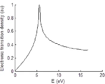
The density of states (DOS) and thus the absorption spectrum of graphene can then be computed. Figure 1.12 displays the density of possible electronic transitions that is closely related to the absorption spectrum. This transition density peaks at 5.6 eV whereas experimentally the absorption spectrum of graphene peaks at 4.6 eV . This band is usually referred as the graphene van Hove singularity.
For simplicity purposes the 2D dispersion relation of graphene electrons will be pro-jected on the kx axis in the following. We discretize the dispersion relation of graphene by
a orthogonal base of eigenvector states corresponding to k wavevectors. The orthogonal characteristic is given by the orthogonality of propagating waves with different wavevec-tors (Fourier decomposition). The state defined by the wavevector k has an energy e(k) defined by the dispersion relation of graphene electrons.
1. SUPRAMOLECULAR SELF-ASSEMBLIES AND OPTICAL ABSORPTION
Figure 1.11: Electron dispersion relation in graphene in a tight-binding model.
Figure 1.13: Density of transitions for the coupled unperturbed graphene-dye system. photon absorption in the dye (blue), in graphene (black) and simultaneous absorption in graphene and the dye (red).
In the following, we make a notation distinction between state of energy above or below the Fermi energy EF that we place at the Dirac cone discontinuity. We note |eg(k) > and
|eg(k)∗ > the state corresponding to the wavevector k that have an energy below and above
respectively EF. We model the dye by a fundamental state of energy E0 and an excited
state of energy E∗
0. We thus define the base of the coupled system graphene-molecule in
four parts to describe all possible states.
|eg(k), 0 > , E = eg(k) + E0
|eg(k)∗, 0 > , E = e∗g(k) + E0
|eg(k), 0∗ > , E = eg(k) + E0∗
|eg(k)∗, 0∗> , E = e∗g(k) + E∗0
Figure 1.13 displays normalized density of transitions for an unperturbed graphene-dye system where the graphene-dye HOMO-LUMO gap is 2.4 eV. The HOMO is placed at -2 eV and the LUMO at 0.5 eV. The absorption of a photon is possible in the dye uniquely (blue curve) and correspond to a Dirac at 2.4 eV. The absorption of a photon is also possible in the graphene only (black curve). In this case, the density of transition for graphene corresponds to the one computed for graphene alone. Finally, it is also possible to absorb one photon in a molecule-graphene mixed state that results from their coupling. This process correspond to the red curve in figure 1.13.
The coupling between graphene and molecule dipole moments, µg and µ respectively,
is defined by the coupling constant κ through the perturbation Hamiltonian H1 = κµgµ.
Perturbed energies for coupled molecule-graphene states described above can be then calculated as follow: Eeg,0,p= Eeg,0+ (κµ∗µg)2 eg(k) + E0− e∗g(k) − E0∗ (1.33) Eeg,0∗,p= Eeg,0∗+ (κµ∗µ g)2 eg(k) + E0∗− e∗g(k) − E0 (1.34) Ee∗ g,0,p = Ee∗g,0+ (κµ∗µ g)2 eg(k)∗+ E0− eg(k) − E0∗ (1.35)
1. SUPRAMOLECULAR SELF-ASSEMBLIES AND OPTICAL ABSORPTION
Figure 1.14: Density of transitions for the uncoupled unperturbed (plain lines) and per-turbed (dash lines) graphene-dye system. photon absorption in the dye (blue), in graphene (black) and simultaneous absorption in graphene and the dye (red).
Ee∗ g,0∗,p= Ee∗g,0∗+ (κµ∗µg)2 e∗ g(k) + E0∗− eg(k) − E0 (1.36) Figure 1.14 displays the dispersion relations of electrons for perturbed and unper-turbed coupled molecule-graphene electronic states.
|eg(k), 0 > (respectively |eg(k)∗, 0∗ >) states are shifted to lower (resp. higher) energies
regardless of the wavevector. A gap is thus opened at the graphene Dirac cone location. When e∗g(k) − eg(k) > E0∗ − E0, |eg(k), 0∗ > (resp. |eg(k)∗, 0 >) states are shifted
to lower (resp. higher) energies. When the inequality is inverted, |eg(k), 0∗ > (resp.
|eg(k)∗, 0 >) states are shifted to higher (resp. lower) energies. If e∗g(k) − eg(k) = E0∗− E0,
the energy of the |eg(k), 0∗, p > and |eg(k)∗, 0 > states diverge to infinity. This unphysical
behavior is compensated by the fact that the density of state is null since the slope tends to infinity.
The resulting density of transitions for the unperturbed and perturbed graphene-dye system is displayed in Figure 1.14. One photon absorption in graphene and mixed molecule-graphene state are shifted to the blue due to the lowering of the |eg(k), 0 >
states and the increase of the |eg(k)∗, 0∗ > states. The Van Hove singularity absorption
band is thus blue-shifted. The transition in the molecule alone is shifted to the red. In fact, the higher transition density of graphene electrons at energies above the dye energy gap explains the overall red-shift of dye transitions. Computations also reveal that a transition is now possible in the molecule at higher energy (approx. 5 eV). However, the density of transitions at this energy is much lower than the low energy transition. Finally, the distribution of electronic graphene states in energy explain a broadening in the dye electronic transitions. These results are coherent with the simpler sovent-dye coupling model since they retrieve the shift to the red of the dye transition.
This analysis estimates the energy perturbation of electronic states of graphene and an adsorbed molecule on top of it. However, it considers the interaction between one electron of the molecule and one electron of graphene. Since the supramolecular network do not covers entirely the graphene surface, one should renormalize the effect on graphene states taking in account the number of affected states over the total number of states. In π-conjugated aromatic systems, one electron per carbon atom participate in the sp2
delocalized electron cloud. The PTCDI core displays 24 conjugated carbon atoms, and forms a supramolecular network on graphene with a 0.5 molecules/nm2 surface density. Therefore, the assembled monolayer have a 12e−/nm2conjugated electron surface density.
The graphene has two conjugated electrons per unit cell, corresponding to a 39e−/nm2
conjugated electrons surface density. Therefore, only one third of graphene electrons are perturbed as described by this model and the rest of electrons are not affected by the presence of the supramolecular network.
This model shows that a clear energy shift for all graphene transitions should be produced by the coupling. Since this energy shift is not observed, we can confidently say that this coulombic coupling plays a minor role in the photonic properties of self-assembled PTCDI-C13 on graphene.
1.3.2 Change of molecular conformation
The overlapping of neighbor carbon atoms sp2 orbitals in organic molecules allows the formation of a delocalized electron cloud that can be resonant at excitation frequencies in the visible range. When sp2 orbitals are twisted with reference to each other, their overlapping decreases resulting in a shortening of the electron cloud delocalization length. Since the delocalization length determines the resonant frequency of the oscillator, the twist of sp2 orbitals produce a color shift in the absorption spectrum of the dye molecule. In a classical framework, a capacitance oscillator sees its resonant frequency shifting to the red when the distance D between charges increases (ω ∼√D demonstrated previously in a 1D model). An increase of the electron cloud delocalization length in an organic dye will shifts its resonance to the red, whereas a decrease of the delocalization length will shifts its resonance to the blue.
Although the interaction between a geometrically complex solvent and an organic dye is hard to imagine, the interaction between a flat surface (like graphene) and an organic dye is easier. One can expect the flattening of the aromatic dye through the π-π interaction with the surface. This effect should result in an increase of the delocalization length and thus a red-shift of the dye resonator.
An interesting case is the adsorption of conjugated dyes on carbon nanotubes. In the axis of the nanotube direction, the delocalization length of the electron cloud should be increased, like on graphene. However, in the perpendicular axis direction, the curve of the nanotube should bends the aromatic dye resulting in a decrease of the electron cloud delocalization length.105
A substrate-induced planarization was invoked for hydrogen bonded porphyrins on h-BN.56 However, the PTCDI molecule already present a rigid intrinsically planar covalent
structure and substrate-induced planarization cannot explain the even larger shift observed here.
1.3.3 Electronic interactions
Electronic interactions between conjugated π-electron systems of molecule and graphene (π-stacking), as evidenced by STM spectroscopy for non-alkylated PTCDI,80 or by DFT computations106 may also play a role in changes of the optical bandgap.
When HOMO and/or LUMO orbitals of a dye are participating in the dye adsorption process to a conductive or semiconductive (including pi-conjugated) substrate, one can expect a dramatical change in the electronic properties of dye through quantum interac-tions.
The charges can be redistributed between the interacting systems, and new coupled states can be created such as mixed charge-transfer (CT) and Frenkel excitons with inci-dence on optical properties.
Unlike Frenkel excitons arising from the Coulomb interaction between induced dipoles at molecular sites, charge-transfer excitons result from the overlap of nearest neighbor molecules orbitals wavefunctions. However, at required distances for the CT exciton to