DC to DC Power Conversion Module for the All-Electric Ship by
Weston L. Gray B.S., Electrical Engineering
University of Akron, 1999
Submitted to the Department of Mechanical Engineering and the Department of Electrical Engineering and Computer Science in Partial Fulfillment of the Requirements for the Degrees of
Naval Engineer and
Master of Science in Electrical Engineering and Computer Science at the
Massachusetts Institute of Technology June 2011
© 2011 Weston L. Gray
All rights reserved
ARCHIVES
SSACHUSETTS INSTITUTEOF TECHNOLOGY
JUL 2 9 2011
L IE
The author hereby grants to MIT permission to reproduce and to distribute publicly paper and electronic copies of this thesis document in whole or in part in any medium now known or hereafter created.Signature of Author... ..
Weston L. Gray Center r Ocean Engineyring, Department of Mechanical Engineering
Certified By .... . . .r. ... ...
P e oChrys Chryssostomidis
Professor of Mechanical Engineering and Ocean Engineering
CertifiedJames L. Kirtley Jr.
Professor of Electrical Engingr ng and Com t Science
A ccepted By ... . ....
Accepted By...
/
C/
Department of
av al
Chairman, Committee on Graduate Students Department of Mechanical Engineering
... Leslie A. Kolodziejski Chairman, Committee on Graduate Students Electrical Engineering and Computer Science
DC to DC Power Conversion Module for the All-Electric Ship by
Weston L. Gray B.S., Electrical Engineering
University of Akron, 1999
Submitted to the Department of Mechanical Engineering and the Department of Electrical Engineering and Computer Science in Partial Fulfillment of the Requirements for
the Degrees of
Engineer in Naval Architecture and Marine Engineering and
Master of Science in Electrical Engineering and Computer Science
ABSTRACT
The MIT end to end electric ship model is being developed to study competing electric ship designs. This project produced a model of a Power Conversion Module (PCM)-4, DC-to-DC converter which interfaces with the MIT model. The focus was on the Medium Voltage DC (MVDC) architecture, and therefore, the PCM-4 converts a MVDC bus voltage of
3.3, 6.5 or 10 kVDC to 1 kVDC. The design describes the transient and steady-state
behavior, and investigates the naval architecture characteristics.
A modular architecture, similar to SatCon Applied Technology's Modular
Expandable Power Converters, was selected as the best balance for the wide variation in loads experienced. The model consists of a standard module that can be paralleled internally to provide for a wide range of system power requirements. Naval architecture parameters, such as weight, volume, efficiency, and heat load, were compiled into a parametric format allowing a reasonable approximation of actual weight and volume as a function of rating and efficiency and heat load as a function of loading. All of the
parameters were evaluated for dependence on the MVDC bus voltage.
Verification of the model was pursued through comparison to available simulations of similar power electronics to ensure that the model provided reasonable time response and shape. Finally, the model met all requirements with the exception of efficiency which was slightly lower than the requirement although several ideas were presented to improve
TABLE OF CONTENTS
A B ST R A CT ... 3
TA B LE O F CO N TEN T S ... 4
LIST O F TA BLES ... 6
LIST O F FIG U R ESS ... 7
LIST O F A B B R EV IA TIO N S ... 9
Chapter 1 Introduction ... 10
1.1 overview ... 10
1.2 background ... 11
1.3 Project G oals... 12
Chapter 2 M odel Specification ... 15
2.1 System Specifications... 15
2.2 Basic m odel structure ... 16
2.3 Pow er Conversion M odule Control... 18
Chapter 3 M odel D esign ... 20
3.1 Base Ship Service Electrical Distribution System Layout ... 20
3.2 PCM -4 functional block D iagram ... 22
3.3 Pow er Converter... 23
3.3.1 Converter M odule Size ... 24
3.3.2 Pow er Sw itch ... 25 3.3.3 Converter Layout... 37 3.3.4 Converter W aveform s ... 38 3.3.5 Converter Efficiency ... 44 3.3.6 Filters ... 53 3.3.7 Capacitor Selection ... 6 1
3.3.8 W ire Selection... 62
3.3.9 Inductor D esign... 63
3.3.10 H igh Frequency Transform er ... 66
3.3.11 Converter Sum m ary ... 72
3.4 Load Sharing...72
3.4.1 D roop ... 73
3.4.2 V oltage Regulator... 74
3.4.3 Load Sharing Verification... 76
3.5 Pow er Control M odule... 79
3.5.1 power Control Module shipwide control and sensing... 79
3.5.2 PCO N m odule PCM -4 Control... 80
3.6 PCO N M odule... 80
3.7 M odel Verification ... 82
Chapter 4 N aval Architecture Param etric Extraction... 83
4.1 Efficiency and H eat Load ... 83
4.2 W eight... 85
4.3 Volum e ... 86
4.4 N aval A rchitecture Sum m ary... 88
Chapter 5 Conclusions ... 89
5.1 Recom m endations for future w ork ... 89
BIBLIO GRA PHY ... 91
LIST OF TABLES
TABLE 1 EFFICIENCY AND POW ER QUALITY REQUIREMENTS [4] ... ... 15
TABLE 2 POWER CONVERTER VARIANTS ... 17
TABLE 3 SWITCH PROPERTIES ... 37
TABLE 4 TRANSFORMER INPUT W AVEFORM ... 39
TABLES CONVERTER SWITCHING MODES ... 40
TABLE 6 UPDATED SWITCHING SEQUENCE...42
TABLE 7 EFFICIENCY FOR 3.3 KV CONVERTER ... 45
TABLE 8 EFFICIENCY FOR 6.6 KV CONVERTER ... 46
TABLE 9 EFFICIENCY FOR 10KV CONVERTER ... 46
TABLE 10 SWITCH SUMMARIES ... 51
TABLE 11 3.3KV POW ER CONVERTER EFFICIENCY...52
TABLE 12 6.5 KV POW ER CONVERTER EFFICIENCY ... 52
TABLE 13 10KV POW ER CONVERTER EFFICIENCY...53
TABLE 14 CAPACITOR PROPERTIES... 61
TABLE 15 W IRE SIZE FOR PRIMARY AND SECONDARY...63
TABLE 16 INDUCTOR EQUATION SYMBOLS ... 64
TABLE 17 INDUCTOR DESIGN SUMMARY...66
TABLE 18 TURNS RATIOS ... 71
TABLE 19 EFFICIENCY AND HEAT LOAD FOR A200 KW PCM AT VARIOUS LOADS AND VOLTAGES...84
TABLE 20 W EIGHT...86
LIST OF FIGURES
FIGURE 1 FUTURE (POTENTIAL) IFTP IN-ZONE ARCHITECTURE [1]... ... ... 11
FIGURE 2 SATCON APPLIED TECHNOLOGY DISTRIBUTED POWER SYSTEMS [3] ... 13
FIGURE 3 BASIC FORWARD CONVERTE R FROM [11] ... 18
FIGURE 4 BASELINE ELECTRICAL DISTRIBUTION SYSTEM...21
FIGURE 5 BASELINE ZONAL ELECTRICAL DISTRIBUTION SYSTEM...21
FIGURE 6 PCM -4 M ODEL BLOCK DIAGRAM ... 22
FIGURE 7 SIMULINK MODEL OF CONVERTER M ODULE...23
FIGURE 8 3.3KV IGBT FORWARD VOLTAGE DROP [12]...27
FIGURE 9 3.3KV IGBT TURN ON LOSS [12]...28
FIGURE 10 3.3KV IG BT TURN OFF LOSS [12 ... 29
FIGURE 11 3.3KV IGBT REVERSE RECOVERY LOSS [12] ... 30
FIGURE 12 3.3KV IG BT SW ITCHING TIMES [12] ... 31
FIGURE 13 6.5KV IGBT FORWARD VOLTAGE DROP [13]...32
FIGURE 14 6.5KV IG BT TURN-ON LOSS [13]...33
FIGURE 15 6.5KV IGBT TURN-OFF LOSS [13]...34
FIGURE 16 6.5KV IGBT REVERSE RECOVERY LOSS [13]...35
FIGURE 17 6.5KV iG BT SW ITCHING TIMES [13] ... 36
FIGURE 18 SECOND ITERATION OF CONVERTER LAYOUT...37
FIGURE 19 BASE TRANSFORMER INPUT W AVEFORM ... 39
FIGURE 20 VOLTAGE CONTROL CIRCUIT WITH ZVS DELAY FACTOR (F) ... 41
FIGURE 21 SECOND ITERATION OF VOLTAGE CONTROLLER...43
FIGURE 22 FINAL VOLTAGE CONTROL CIRCUIT ... 44
FIGURE 23 3300V SW ITCH FORWARD VOLTAGE DROP [17] ... 48
FIGURE 24 3300V SW ITCHING ENERGY [17] ... 49
FIGURE 25 6500V FORWARD VOLTAGE DROP [16]...49
FIGURE 26 6500V SWITCH TURN-ON LOSS [16] ... 50
FIGURE 27 POW EREx 6500V TURN-OFF LOSS [16]...50
FIGURE 28 POW EREx 6500V REVERSE RECOVERY [16] ... 51
FIGURE 29 INITIAL TEST OF OUTPUT FILTER ... 55
FIGURE 30 SHUNT CIRCUIT ... 57
FIGURE 31 SHUNT CONTROL CIRCUIT ... 58
FIGURE 32 FULL LOAD STEADY STATE RIPPLE...59
FIGURE 33 TRANSIENT RESPONSE 33% TO 100% AT 0.04 SECONDS ... 60
FIGURE 35 LIFE EXPECTANCY M ULTIPLIER FOR GENERAL ATOMICS TYPE C CAPACITOR [20]... 62
FIGURE 36 SANDW ICH W INDINGS SHOW ING PRIMARY AND SECONDARY [6] ... 67
FIGURE 37 SIMULATION W ITH 3000V SECONDARY VOLTAGE ... 68
FIGURE 38 SIMULATION W ITH 2000V SECONDARY VOLTAGE ... 69
FIGURE 39 SIMULATION W ITH 1500V SECONDARY VOLTAGE ... 69
FIGURE 40 SIMULATION W ITH 4000V ON THE SECONDARY SIDE ... 70
FIGURE 41 GENERATORS IN PARALLEL OPERATION...73
FIGURE 42 VOLTAGE REGULATOR ... 75
FIGURE 43 REGULATOR FUNCTIONAL TEST...76
FIGURE 44 PARALLEL MODULE OPERATIONAL BLOCK DIAGRAM ... 77
FIGURE 45 PARALLEL OPERATION AT HALF LOAD ... 78
FIGURE 46 PARALLEL OPERATION AT FULL LOAD...78
LIST OF ABBREVIATIONS
BJT Bipolar power Junction Transistors
D Duty Ratio
GTO Gate Turn-Off Thyristors
HFAC High Frequency AC
IGBT Insulated Gate Bipolar Transistors
IPS Integrated Propulsion System
MOSFET Metal Oxide Semiconductor Field Effect Transistors
MVDC Medium Voltage DC
NGIPS Next Generation Integrated Power System
PCM Power Conversion Module
PGM Power Generation Module
PCON Power Control Module
SSCM Ship Service Converter Module
SSIM Ship Service Inverter Modules
ZCS Zero Current Switching
CHAPTER 1 INTRODUCTION 1.1 OVERVIEW
The early stage ship design requires analysis and comparison of many different ship variants. The ships that are designed and then built based on these early studies are a huge capital investment for the country. Many ship designs have a life of 50 or more years by the time the initial design, the construction, and then the service life of the last constructed ship is taken into account. All of these factors add up to the conclusion, the right decisions need to be made early in the design of a ship.
The early stage designer is usually working his designs to meet a set of
requirements which are outside his control. Additionally, they have to produce affordable designs that are the convergence of maximum durability, mission capability and
survivability all at a minimum cost. Ship designs are the definition of a systems
engineering problem with many designs rivaling the complex integrations of the world's most complicated systems.
Much of the early stage design is completed by wise individuals with multiple decades of experience. They have developed artful techniques and gut feelings that
produce very good results. The purpose of the "MIT End-to-End All-Electric Ship" model is to supplement these talented individuals by providing a tool which can show higher level simulations of a ship system with a minimum amount of set-up time.
The design tool was set up to allow these early-stage designers to make good choices with better information. The end goal was to provide system wide modeling of a new ship design.
This project designed a model of one of modules in the ship's electrical distribution system. This module, a Power Conversion Module (PCM)-4, converts the main bus voltage,
3kV to 10kV, to 1kV DC to supply loads and other power conversions modules throughout
the ship. The model provides transient responses for evaluation. The Naval architect also needs data on the efficiency, heat load, weight and volume of the component. The
physics-based model was used to develop a set of parametric relationships to answer these questions.
1.2 BACKGROUND
The Navy has produced a roadmap of its view of technology development in the area of electric ships utilizing an integrated power system. Published in the Navy's Next
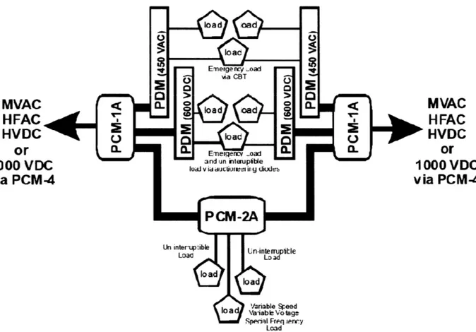
Generation Integrated Power System (NGIPS) roadmap [1], the roadmap was used extensively to produce the high-level characteristics of the PCM-4. The roadmap also projects a more compact integrated propulsion system (IPS) layout. This next IPS layout was utilized in this model, and the operation and major components are outlined below. Figure 1 shows a notional electrical distribution system architecture.
load oad
load
V Emerge ncy -oad
xia CBT
C1 > -> 0
MVAC a- gL loa Cod MVAC
HFAC 1 od dH FAC
HVDC
loadHVDC
or
-
Emerency
_oad
-or
an
n interupib in uple
1000 VDC J0dJVi d3iJ3:-1 lydidt 1000 VDC
via PCM-4 via PCM-4
P CM-2A
Un inter-utble U -nem ll
load
load
lod Variable eed
load aiabl *Otag
Spenial Freq uerty Load
Figure 1 Future (potential) IFTP in-zone architecture [1]
The PCM-4 is used to convert the main generation voltage to 1000 VDC which is supplied to the PCM-1A. In this specific application, the PCM-4 will also contain the control center which will coordinate the power available and the amount of loading that is allowed to run downstream. The NGIPS refers to this unit as the Power Control Module (PCON).
"The PCON module consists of the software necessary to coordinate the behavior of the other modules [2]."
The PCM-1A is made up of a variety of Ship Service Converter Modules (SSCMs) and Ship Service Inverter Modules (SSIMs) which supply power to the individual DC and AC loads. These loads can be powered from more than one PCM for reliability via
auctioneering diodes or a bus transfer switch. The individual modules can be paralleled together to supply larger loads. Additionally, the modules would ideally be available in a number of different power ratings to allow for the maximum efficiency and minimum cost to power any additional load added to the ship.
The PCM-2A is a smaller Converter that could even power and be located with a single load. The PCM-2A would replace large motor drives and be able to output variable frequency AC as well as supply smaller uninterruptable loads with redundant power. The redundancy would be achieved by powering the PCM-2A from both buses in a given zone. However, the PCM-2A would not be a redundant component; although, redundant modules could be included in a PCM-2A for the most critical loads.
In general, this next step in IPS architecture would minimize cabling by only requiring the main distribution system lines to cross zones to power each zone's PCM-4. For certain loads, it would also reduce the number of power stages required to supply power to a load, specifically DC loads. Finally, this architecture allows the reduction of the number of motor drives throughout the ship by supplying a common method to drive large motors which could easily be integrated into the electrical distribution system's control network.
1.3 PROJECT GOALS
There are nearly as many power conversion designs as there are power supply designers. Nevertheless, there are a limited number of different power converter structures which can then be implemented with a variety of components and different options. For this project, the concern is not only the power converter design, but also the PCM-4 design which must be able to take power from a variety of input voltages and
The PCM-4 for this design must include variations for 3kV to 10kV input with power rating variable between 1 and 5MW. The PCM-4 was divided up between the controller and the modules. The PCM contains one controller which performs several critical
functions. These functions include maintaining the voltage setting of the individual power modules to maintain 1000V DC output. In addition, the controller would ensure smooth operation of the ship's electrical distribution system.
Zonal Distribution Figur Early on selected. These loads. Using th the number var
A key co converter envis The switches m experience in t avoid damagin switching to oc Main Propulson
ZONE 1 ZONE 2 ZONE N 800 VDC - 4SO VAC
PMR DC nyerterw
DC -DC CONVERTER DC -DC CONVERTER DC - DC CONVERTIR
0 350 -800 Vdc
45
4SVac 30
100 Vd DC - AC INVERTER DC -AC INVERTER DC - AC IN , 350 -800 Vdc
1000 vde 1 1000 Vde
DC - DO CONVERTE DC - DC CONERTR WC - Dr. 8ON1R"E
1000-800 VDC
4160 Vaw 3+ Converter
e 2 SatCon Applied Technology Distributed Power Systems [3]
the power conversion strategy from SatCon Applied Technology was PCMs use small modules which can be connected together to supply larger ese ideas, the PCM-4 could be made up of a small number of modules where
ies depending on the total load the PCM-4 is expected to supply. mponent of any power converter is the solid state switch. The power
ioned here is a switching type of power supply using Silicon based switches ust be able to survive the maximum current and voltage difference they will he converter design. Additionally, the switches must be kept cool enough to g the switching structure. Finally, the switches must be set up to allow the cur when there is no voltage and current on or through the switch.
Depending on the specific component used, there are various other losses which must be minimized.
From a technology point of view, the other components of the PCM, inductors, transformer, computer control, are all very well established. The technology of the
switches is the component that is still being improved. This continuing improvement offers a chance for future capability in terms of voltage limits, current capacity, and efficiency improvements, but it also supplies a host of unknowns which must be dealt with in the modeling process.
CHAPTER 2 MODEL SPECIFICATION
2.1 SYSTEM SPECIFICATIONS
The model will have to conform to the same transient limits and other specifications as a shipboard PCM. This will allow the model to provide useful results when coupled with the other systems of the all-electric ship model. The specifications to be met are outlined in this section along with the basis used to determine these specifications.
The Navy's NGIPS Roadmap indicates that the PCM-4 and PCM-1 will likely be replaced by a PCM-1A which performs both tasks. With this in mind, this project will attempt to make the PCM-4 modules such that they can be easily combined with a future PCM-1 to maintain a consistent architecture with the Navy.
While Navy Specifications for their systems are not available in open literature, a reference was found in the SBIR Program. The Navy is requesting design work on power conversion devices that meet the requirements shown in Table 1. From the description, these requirements are perhaps a bit conservative, but they should be representative of what will be expected of future naval combatants. Only the threshold values were used in the table below to simplify the design process.
Parameter Threshold Condition
SS Voltage Regulation +/- 3.5%
Transient Voltage Regulation +8.5%/-16.5% 0 to 50%, 33 to 100% and 100 to
0% at 70 MW/sec
Conversion Efficiency 75% 20% rated load
Conversion Efficiency 96% 35% rated load
Conversion Efficiency 96.5% 40 to 100% rated load
Steady State Ripple Voltage 2%
Table 1 Efficiency and Power Quality requirements [4]
The controller and converter circuitry work together to produce an easily
controllable output voltage. In addition, the output from the PCM-4 will be used to drive another power conversion stage which will produce a particular voltage required by a load.
2.2 BASIC MODEL STRUCTURE
Selecting the structure of the model is a much more complex question than simply selecting the best of several options. Like the rest of ship design, the converter design is a complex systems engineering problem. This implies that many of the parameters for the converter depend on each other, and an optimal converter for one use is a poor choice for another use. This selection is being made for a converter operated in the all-electric ship as explained above. Efficiency, reliability, size and weight are all important considerations which must be traded off against each other to select the best converter structure.
On a circuit level, there are more specific concerns that must be optimized. The size of the energy storage components should be minimized. Additionally, minimizing the stresses applied to the switching components will allow smaller and/or cheaper components to be used and/or will increase the operational life of the converter.
Losses must also be minimized to increase the converter's efficiency. Switching losses, conduction losses, and field losses must all be analyzed and minimized.
After the model has been completed, details such as the power capacity of each module and component selection will be determined. Some level of optimization will be performed for the output power level based on number of units for given maximum power and efficiency. Finally, the components will be selected and/or designed. The actual component parameters will be input into the model and used to validate all component assumptions made during the design phase.
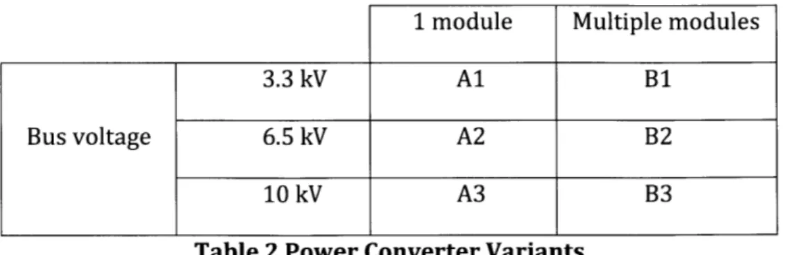
The different types of power converters have their relative advantages [5]. The Direct Converter has significantly lower switch stresses than the indirect converter topology. Additionally, the Direct Converter requires about half or less of the energy storage that an indirect converter requires during reasonable operation. Therefore, the direct topology will be utilized in this model.
1 module Multiple modules
3.3 kV Al B1
Bus voltage 6.5 kV A2 B2
10 kV A3 B3
Table 2 Power Converter Variants
As shown in Table 2, the conversion ratios will be from 0.1 (10kV input) to 0.3 (3kV input). While 0.3 might produce reasonable switch stresses, the reduction in voltage from
10kV produces too much switch stress for a single stage design. One possible method to
reduce the switch stresses is to add a transformer to the direct converter. This type of converter is called a forward converter. In addition to reducing the switch stresses, the transformer also provides electrical isolation between the input and output. This feature could be significant for the high voltage system, especially during a fault induced transient.
The basic forward converter is shown in Figure 3 below. The operation of this forward converter really only draws power from the source for half of the cycle. When the switch is on, the source supplies current to the transformer which charges up the filter elements on the secondary side. For the second half of the cycle, the filter elements solely supply the load. This type of converter works well, but it requires a mechanism to reset the transformer on the primary side. Resetting the transformer refers to reducing the flux to zero during each cycle to prevent a buildup of flux and saturation of the core. Additionally, the basic forward converter also requires relatively large filter components to maintain a constant voltage on the secondary side, especially at low switching frequencies.
Figure 3 Basic Forward Converter from [11]
To minimize both of these limitations, a different approach was tried. The high power switches have a relatively low switching frequency; this characteristic will tend to increase the size of the energy storage components. As a result, full wave rectification was chosen for the secondary side. To utilize a full wave rectifier, it was realized that the
transformer flux must not only be reset, but it must be reversed. This was accomplished on the primary side of the transformer by modifying the inverter. Using a different switching configuration, it was hoped that the transformer primary could be reversed yielding an AC voltage on the secondary which would be suitable for full wave rectification.
Based on the above considerations and research, the Forward Converter was selected for converter topology. This topology should minimize the switch stresses
allowing a larger input voltage and longer component life. Also, the lower voltage switches are easier to develop if they are not already commercially available. The forward converter also limits the amount of stored energy required which will minimize the size and weight of the required inductors and capacitors in the filtering of the converter.
2.3 POWER CONVERSION MODULE CONTROL
The desire to enable the ship to reconfigure itself in response to damage or system failures requires a networked power system. In addition to the reconfiguration options, the networked controllers enable the different electrical distribution components to respond very quickly.
starboard bus. The switch is an electrically controlled bus transfer switch. With the size of the filters required in the power supply, the assumption is that the switching of source voltage could be done with loads energized.
A quick controller allows the system to respond many times faster than the cycle
speed of the machines at the sources or loads. For example, if a power generation module (PGM) powering the PCM-4 was tripped on a fault, the PCM could instantly determine to switch its source to another bus. An additional option is the PCM-4, working with the other PCM-4's, could determine that the loading is too much for the remaining PGM, and the PCM-4 could initiate load shedding through the PCM-1 and 2 modules. A fast controller and efficient control codes could enable these changes to occur before the bus voltage has had a chance to drop appreciably or a circuit breaker is tripped.
The PCM-4 power conversion modules must operate in parallel to supply the total PCM-4 loads. In addition, the PCM-4 power conversion modules will have to share loads with other PCM-4's. These features will have to be included in the control system.
CHAPTER 3 MODEL DESIGN
To meet the specifications determined in chapter 2, the converter will have to be carefully designed. The input and output filters will be designed and tuned to result in a high efficiency while meeting the input and output requirements. Additionally, the
switching losses must be reduced to allow the converter to function at a higher efficiency. Finally, the components required to perform these functions must be selected and/or designed. It is recognized that some of the components may not exist, especially for the higher bus voltage, but projected values will be used for components not commercially available.
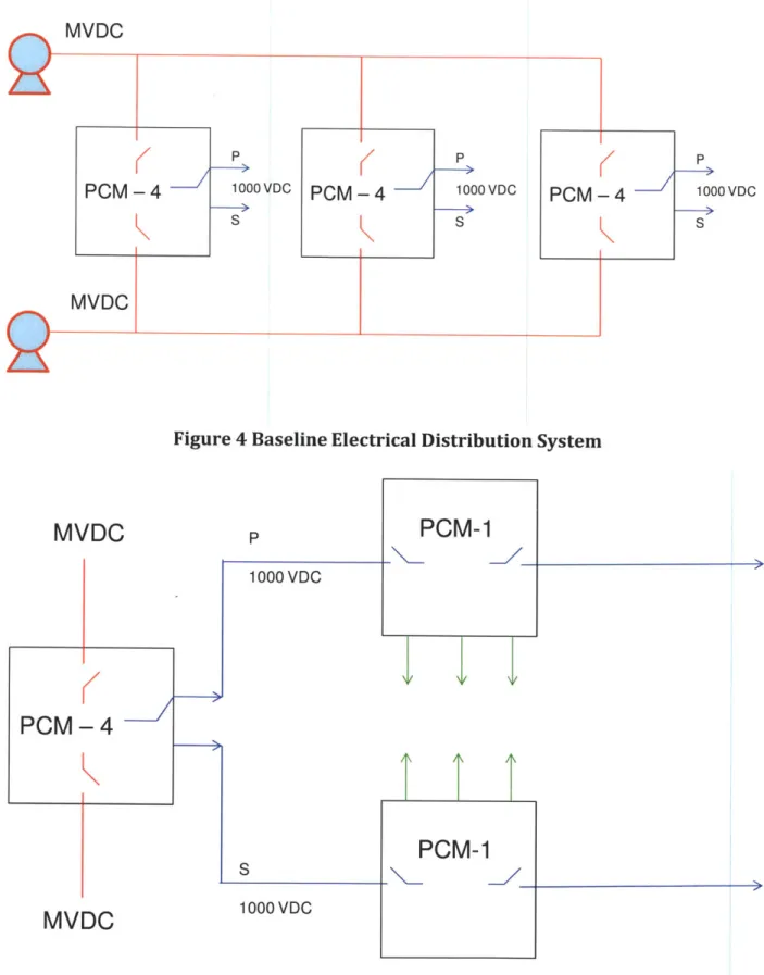
3.1 BASE SHIP SERVICE ELECTRICAL DISTRIBUTION SYSTEM LAYOUT
Using the general guidance developed in Chapters 1 and 2, a baseline electrical distribution system layout was developed as shown in Figure 4 and Figure 5. This baseline attempts to demonstrate the reliability features and general configuration that is
envisioned to operate around the PCM-4 designed herein. A simple 3-zone ship is shown for emphasis only.
MVDC
Figure 4 Baseline Electrical Distribution System
MVDC
PPCM
- 4
1000 VDC 1000 VDCMVDC
PCM-1
PCM-1
The baseline configuration has a port and starboard MVDC bus which feeds the PCM-4's. This provides reliability in that all the PCM-4's can be supplied with power independent of which set of generators in online. Likewise, the PCM-4's output of 1000
VDC is fed to a port and starboard ship service bus. Typically, the port and starboard ship
service buses will be fed by half of the PCM-4's to increase redundancy. Inside each zone, the PCM-1's will be supplied by the opposite bus. Individual loads will then be supplied from the PCM-1 or PCM-2's with vital and redundant loads powered from multiple sources.
The net effect of these reliability considerations is an electrical distribution system that can get electrical power from any available source to any available load through any available PCM configuration.
It should be noted that there are multiple configurations that the PCMs can be
arranged in. For example, the PCM-4 could be combined with the PCM-1 to form a PCM-1A. There could be 2 PCM-1A's per zone to produce a redundant system with, perhaps, a
different survivability characteristic.
3.2 PCM-4 FUNCTIONAL BLOCK DIAGRAM
Simulink is the primary modeling tool utilized for this project. As such, the PCM-4 is made up of subsystems: PCON and converter modules. The converter modules are further broken down later. The overall PCM is shown below in Figure 6. More converter modules can be added in parallel to supply larger loads.
Enuous po we rg ul
The minimum control signal is a voltage control signal from PCON that sets the operating voltage of the modules. Sensing lines were also required to determine the actual operating voltage of the PCM. These minimum signals are expanded in later sections as the system design is expanded.
3.3 POWER CONVERTER
The first piece to explore is the Power Converter stage. The Power Converter stage is made up of a switch, transformer, and diode as the major components. The power converter stage produces an average output voltage at 1000 VDC. The input and output filters work with the Power Converter to produce a voltage with a limited amount of ripple,
2% of steady state voltage. The converter is shown in Figure 7 below.
N:1 Continuous powergui D1 D2 D3 D4
Figure 7 Simulink model of Converter Module
The forward converter consists of a direct converter and a transformer. The direct converter produces an AC voltage with four switches. Therefore, even though the input and output of the converter are DC voltages, the switched AC voltage allows the use of a transformer in the middle of the converter, which transforms the voltage to the level
out gnd
required to produce the desired output voltage at the ideal duty ratio (D). The ideal duty ratio value depends on the switch used and the circuit, but in general the ideal duty ratio reduces stress on the switch and maximizes efficiency. Typically a 50% duty ratio or D of
0.5 is a good tradeoff.
The type of converter shown above is sometimes referred to as a double-ended isolated forward converter. In addition to the advantages mentioned above, this converter also reduces the voltage ratings required for the switches. Based on the current level of switch technology, it is still expected that the higher MVDC bus voltages will require circuit modification to achieve a realizable switch voltage rating.
3.3.1 CONVERTER MODULE SIZE
The PCM-4 high level architecture decided on earlier was a Converter made up of a control module and the needed number of converter modules. To complete the design of the PCM-4, the size of the individual converter modules had to be determined. This size was bounded on both the lower and upper ends by physical considerations inherent in the ship and the electrical distribution system
The size of the converter modules was determined to be large enough that the design for paralleling the multiple modules was not overly complex. Too many modules operating in parallel could have led to unexpected interactions. Additionally, it was
believed that having too many modules would decrease the overall efficiency of the PCM-4. On the other hand, having too few modules would also impact efficiency by ensuring that an individual module would rarely be operated at its ideal loading. The requirement to have an installed spare module would also become cumbersome if the modules were too large.
Initially, an in-depth optimization was planned for the module size. However, it quickly became apparent that the number of variables from zone loading to ship type made the prospect of optimizing the module size for any one configuration unproductive. As a result, the possibility of multiple module sizes was introduced, but a 200 kW module size was selected as the initial offering. This size was intended as a compromise between the
previously mentioned parameters as well as trying, in advance, to limit the size of the filtering components.
3.3.2 POWER SWITCH
The type of switch selected for this design affected all of the other components and even influenced the converter layout. As a result, after exploring the basic transformer frequency ranges, the switch selection was the next step. The proper switch selection was critical to the efficiency and durability of the converter.
There are several types of switches to choose from. Common designs include variations of Gate Turn-Off Thyristors (GTOs), Insulated Gate Bipolar Transistors (IGBTs),
Metal Oxide Semiconductor Field Effect Transistors (MOSFETs), and Bipolar power Junction Transistors (BJTs). Each of these devices has advantages and disadvantages that were explored to select the best device for the PCM-4. Silicon-Carbide (SiC) devices were not seriously considered due to the lack of established devices. As larger SiC devices are produced and tested, their advantages should be reviewed for inclusion in this type of
converter.
GTOs can handle high currents and high voltages, but they require commutation or high turn off currents [7]. As a result, they were placed at the bottom of the component selection.
Barkhordarian [8] provides a comparison of BJT and MOSFET devices as follows. BJTs are current driven devices, and as a result, as much as 20% of the collector current is required to keep the device on which drives up the cost and complexity of the switching circuit. In addition, BJTs have a relatively slow switching period and are difficult to operate in parallel. MOSFETs by comparison are faster switching and can be paralleled easily due to the forward voltage decrease with temperature increases which helps to evenly
distribute the current to each parallel device. However, the forward voltage drop at high voltages becomes worse than BJTs which limits the effectiveness of MOSFETs.
IGBTs are a combination of a FET and BJT. As a result, IGBTs are voltage controlled devices that do not require a snubber circuit. IGBTs can also be combined in parallel to provide added current capability [7]. The IGBT also has the low on resistance of a BJT and
higher current capability than a MOSFET [9]. As a result, IGBTs have become "the
switching element of choice" in high voltage applications. Although the IGBTs have a lower frequency range than MOSFETs, recent advances have increased the frequency range of IGBTs while minimizing switching losses. As a result of these characteristics, the IGBT was the first choice for a switch for the PCM-4 model.
To provide a safety margin for survivability, a factor of 2 was used for the switch rating. For example, if 6 kV was expected across the switch during normal operation, the switch or switches must be rated at 12 kV. Not only does this provide an inherent
capability to survive voltage transients, but it also improves the switch life.
The highest rating IGBTs commercially produced were rated at 6500 VDC. Of course, this voltage rating would not support the 10 kV model variant and provide the safety factor of 2. As a result, two options were considered. The first option was to assume that eventually a higher voltage rating IGBT would be produced. The second option was to use the IGBTs in a scheme that would allow an effective voltage splitting between multiple IGBTs.
The first option appeared to be low risk. Based on the literature review, a 10 kV switch appears to be the next iteration of the IGBT design. The second option evaluated allowed for operating IGBTs in series. Ju Won Baek [10] presents a simple and efficient series connection which was used as a starting design for series switch connection. He uses an RC circuit to balance the voltage across 2 switches and allow for a higher operating voltage.
The variants shown in Table 2 will be analyzed individually starting with variant Al which is a single module operated at 3.3kV input voltage. In order to achieve the 2 times rated voltage, at least a 3kV switch must be used since 2 switches are in series. As
estimated in Equation (1) below [5], the switch current is approximately 128 A.
P = pf - I, = 2(200kW) =2P 128A (1)
2 Pf= P Vppf -3300V(0.9S)
The Hitachi 3.3kV switch referenced for this paper has a current rating of 1500A providing a comfortable current margin. The higher current and voltage rating will also
allow the converter module to absorb a rather large transient without damage to the switches. As shown below in Figure 8, the forward voltage drop is approximately 1.3V at a
worst case 125"C. Figure 9 indicates that the turn on loss will be approximately 0.4
J/pulse,
and Figure 10 indicates an approximately 0.35
J/Pulse
turn off loss. Finally, the reverserecovery losses will be approximately 0.35
J/Pulse
as shown in Figure 11. The turn on timeis approximately 1.9[tsec with a turn off time of about 5.8 psec as shown in Figure 12.
TYPICAL| 3000 2500 2000 LL 3 1500 -o 0 1000 500 0 VGE=OV -Tc=25 'C - --- 12 Tol 25 C50 -- TG 150C C_ 0 1 2 3 4 Forward Voltage, VF(V)
4.0 3.5 3.0 2.5 0 (n 2.0 (P2 0 0 a- 1.5 PR-0 200 400 600 800 1000 1200 1400 1600
Collector Current, IC(A)
Figure 9 3.3kV IGBT Turn on loss [12]
TYPICAL -[EConditional Ls=10-nH Eon(full) We- I aS! -va-t av Eon(fu--0 R13=2.79 CGE=330nF (10C) Tc=125"O Eon(1 0%) 0 ' t 7t3 4 12 Eon(0) -7 (exC)- dt
4.0 3.5 3.0 S2.5 CL U S2.0 0 C 1.5 1-0 200 400 600 800 1000 1200 1400 1600
Collector Current, Ic(A)
Figure 10 3.3kV IGBT Turn off loss [12]
T Y PICALI [Conditions] Vow= I IIOV -- Ven d0V v-*15v CGE=330nIF _ TU=t25te
.of(tA) = PICA vee a
E-off (full) =((k -VCEQ.
Eoff(full)
Eoff(ful)
(150 c)
Eoff(10%
3.0 2.5 UD 0 -1.0 0.5 0.0 TYPICAL [Conditions) _ea I lH VeeGt 650V VG=*1 5V RG=2.7Q CGE=330nF Te125%C Err(full) -(150 C) Err(full) Err(1 0%) t11 110 --Err(10%.)= c l xVe) .dt -Err(full)= (1,x VCE)-d 0 200 400 600 800 1000 1200 1400 1600
Forward Current, IF(A)
TYPICA L 6.0 1 1 Lon dition - - -- - - ~ALa100fnM - - - c=1UUIIV -VG-*I5V G=2.70 5.0 0-E- 330oF Ta=12 4T toff 4.0 - ~~ ~ ton 0 --E 1.0 trr 0.0 -0 200 400 600 800 1000 1200 1400 1600
Collector Current, IC(A)
Figure 12 3.3kV IGBT switching times [12]
A larger switch was required for variant A2. In order to achieve the 2 times rated
voltage, at least a 6kV switch must be used since, again, 2 switches are in series. As estimated in Equation (2) below, the peak switch current is approximately 65 A.
I = 2P _ 2(200kW) - 65A (2)
2 P Vppf 6500V(0.95)
The Hitachi 6.5kV switch referenced for this paper has a current rating of 750 A providing a comfortable margin. As with the 3.3 kV switch, it is believed that using the larger switch at a lower than rated power increases the operational life and reliability. As shown below in Figure 13, the forward voltage drop is approximately 1.4V at 125"C. Figure
14 indicates that the turn on loss will be approximately 0.8 J/pulse, and Figure 15 indicates an approximately 0.6 J/Pulse turn off loss. Finally, the reverse recovery losses will be
approximately 0.55 J/Pulse as shown in Figure 16. The turn-on time is approximately 2.3 ptsec with a turn off time of about 5.8 iisec as shown in Figure 17.
TYPICAL 1400 1200 1I000 6T4 800 0 0 1 2 3 4 5 6 Forward Voltage, VF(V)
Figure 13 6.5kV IGBT forward voltage drop [13]
I I till I I I II I i i i
i=ll I i liii
Tc=-1251C -- ~|
-1- ~1 -t TT T T T T T T
-LLLL .. L WL l-_IJJ J J -J.J L. 1 .
i i II i i i i iii Ilti I Ii i l I i ii|
-4---- -4--4-4- -4-4- -4-4--4- -4-4-4-i-
-4-4-4-4-111 i i i i iii i I 1 i t1 I i l
F~rFr ~t-i-Fl----l" ~ -T T T T TT T
lilt ii lllt t1ill fill lilt liii lilt fi i ii I i i I i I i iii
i ii i ii ilt I i ii i ii Ill t Iill
Sil i i i i ilt t I ilt I ii i i t I ill F 1 1 -11 T~TT T T T T T
LLLL -LLL.WtJ- JJ JJ. 1.. j1iLL
till fil l fill Ill l1 liii 1111
- l-1-4_ -E - - -lt i1 - 1 - -4-4 -4 - + -+ + + - -+ + ++ . I I I i ii i ii i i i i ii
-in- ~-T Tr ~-
-T-T-T-r-mTT-ilt i ii I lil Itii i iii til ll I ill
iIi i ill ilt I I ill t iill t Iill
-L-LL -Li-t---i---1 4 4 -J.-4.4. LLA. lilt~_ til til I it tiltlltl
l iI i i i iltI I I til i i ii i i i
LLLL LLL LL- JJ. JJ J 1. 1 1Lii
I- - -F - I---1-1----i- -+- --i - --i + +
+1--I-i-I i l l ii 11li t 1l lilt ilt 1 fill ~lFrFF -rrl-~--~~ -- ~-1 77 -1i1 T~TT T T TT'
_LL_ IL-L WJ _L _L - - L
till 1 iii liltl f t l ii il I li
LLLLP I-i-i--I-I- --J.JJ 4444 LJ.Jr. 4T
rLi-lilt fIll I I fi 1111 i it l it iii
t-r-r-t- i-i-i-i--ii i--i--ii - i-t- -t-| i| i | --1 |-| F F Fi I I I I I 11 -1 1 111 T T T T T - i-- I-i-i-i 1-1- - -4 -- 4 - -4 - -t -4 - + - + + + + + FFFrr r- - - ----1-1-1-1- -T--1 - TT T TTTT' LLL -l __LL-U--JJ . JJ..l J.14l . .L.LL I I I I i t i J j I i I I I I l I I I I - F F F
TYPICAL II~~~ II I I i I 14.0 12.0 10.0 I I I I -4--4-_ T L I r T I I -FT I I - L. I I - T Li I I I I --- l-iI I I I I I -lJ.JJ_ I i I l i I lii til Ili
I i ii I i ii i ii lilii 11
-- l+- i-+- - -11-1-- - - -- i-I- --I--I -FT T-r- -- -r Tr T T~ -1 -1- rrr T-1-1
lI I I I I I I I I jill
i i IIi Il l|i lii Ili
'±LLL II I IJW WI WL ~F T ~l Tl~~ lT T~ 7r1r 1 Tr 1 fiii I I lI I I L_ I | |
|
| ||
| |I| | WIW LWL LJ LW h I iJ I JI | || TT I I T-T I I T--I T--I T i~ SI ii -I -I -I -I--1-1-1-7
I I I I I I l | F J I I L -Frrr -I i i i I I FF TT -1 L L.Li IJ ' ' I ' I I I I I I I' I I I 1 7' F I-, Ly~I i j I 10i LL. -L LL. J&(0
L 0 250 500 750 1000 1250Collector Current , Ic (A)
Turn-on Loss vs. Collector Current Figure 14 6.5kV IGBT turn-on loss [13]
1500 VGE=±15V, Rg on'g 2Q Vcc-3600V, L4200nH, Tj-I 25 C Inductive load
We
0 n U tVa. 12 Eon(Flil J 1 We cd 0I 4-r-_jI 8.0 6.0 4.0 2.0 0.0 I I -F F - I -I - . L I I I I I I I .1 - I- .L L. I I- I- I I I - [ I I I II I I I I I I - - - I _I- L L. II I I I I I : : : : : : : : ! 4-F - -4 SI I_ J I I I . -1...-1~T-i-1-1-TYPICAL -F-Ft L1 -J-i - L -- --- ' L L J- J --J . L VGE ±15Vgffh2 .-- L L D D -L Vcc 3600VL-2OOnH. Ti 125'C - --- Inductive load - - w--F - t - -1-- L -4-.- 1 LLL L4 . .. L 0 J J- .. LLLI .. .~ aT .1-r a-1-- -II -I
- - Eoff(1O%). Ic-Voeid - -
II---E J 1~ t
L EoffiutjIfk loVce 4_ _ii_ .4 ___ I4- - 4-i Ii 12.0 11.0 10.0 9.0 - -I J. -i-I--4.4 -1+444-4 ---+ _ 1 1 --L A - -1--4- -E 1-E11 J.J-l-1 - L-LL-A. j|Eo MRFull) --4-4-1- 1- -- 4--1-1 1-- -t -4-4-1--1I- - I-- -Eoffi0%)' LLL JJJ-I-LL L L. -4t-4-1--1 - -I- -- I -44-L -44-L -L! L1++ --4-4 --i ~-rr 4 44L -4-4 -4-Id L.L -t 4-I .-C 4-IL4-LL L 4i .1 -44-4-4- :ii-j:- -4-4-1-J- 44----JI JJ - -44-1-1-LE 1 I [E' i i i i :I[E 1111]] E E 1-4 4 D :11 i : 1D-I-Ii--A - 4 --- L L - i i _214 ~- 4-~4-- -4~ -- E ] -- - --]] - I-~LEE ~ -I~[-- t+ - -i-- - -- - -- ---- +-- -i- - r- -r- - - --0 r- -rvrr-TT -7-T-77 JJ 7-T-i:r-F -7]] 0
EETI - JJ~CC~CEll JJJJ~~CE
IE,-:I~[]]-- L.LJ.IE,-:I~[]]-- -_----..LLL lJ LML L . J. J .1J - - 4 - - -4--1- - -e - 4 -t -1--1 - - - - - -+ + 1 i 0 ~ ~ ~ - --- r - r- r--- -r-, r --r-r-r-r - L JJ -1j - 1--1- -. LLLJ L -4J J---...1L L L J.J.J -V --+- 4-- - -F-1-- -- -4 - -4-1- 1- --- e - + i 0 250 500 750 1000 1250 1500
Colector Current , Ic (A)
Turn-off Loss vs.Collector Current
Figure 15 6.5kV IGBT turn-off loss [13]
- L L L L
-ILL L L
-i.-
I TYPICAL
5.0 ,, 1eae' 11
-r T VGE ±15VRgon, 32Q -i---rrr -r T T
- T Vcc 36COVL-2OOnHTj 125C -i--i-rrr
TT--F-T ltduA ve luid ii- r T T
-F T -rTl F F4.5-r-r-FTI If ~FT F1 L . 4.0 -r1 -I F T - Fr'r TT F T:t12 1--F F TT 3.5 1 F~ FtT(1O4. f 11F-Vrodt 1 - - -r F I I -T T ITr -T~ -- -r-r--F- FT r T.1 1-1~l- ~rr "-r T
T-F Ef It~Ful.f ID r veet --- i-rrr FTT7
I I iI I I I I I I 1 I 1-~l-1-~l-1-F- FTTTTT --TTl~~ T T T~rF ~T r 7 T I -'-1~ -l1 -~1"TT -i - - r r - T ~-F.5r(1091 ). 1 1 F V1 1 r 1 T I I I I I I I I I I .0 . 0.0) T! T 1 ii I I I I I I I I I I F FT - rT -i lI i T li - |TIii li I i I I I
lii II liii lii i
li i I I liii .l . .. i. I Ii| liii I I I liii li ii i ii _______ l i i Ii iIi i i tI ilt I I1 i i ii li i i I lI i I i iII I iii i ii I Ii i li ii I lii liii i ii i i ii I i i i i | I I li ii li ii i ii l Iiii ______ I iiI IiI III I i i I i i li i I iI I
i iii ili ii l Iiii i ii I Ii ii _____
i II II i Iiii i i i i i i III
ilt II i I i l Ii i I l i i i i ii i I I I iii i i i I ilt I i i I i
| lii i I iii I l Ii i ii i lIi i i Ill
li l I I i I lii i i i i i i Ill
0 250 500 750 1000 1250 1500
Forward Current, IIIA)
Figure 16 6.5kV IGBT reverse recovery loss [13]
10.0 9.0 7.0 6.0 S . C 0 3.0 2.0 1.0 0.0 TYPICA L i- V L 15V Rgo -. I Q L L L-- i
I-I I-I Voc 360DV, L'.200nH, Ij-125"C11 lii i
- - Indtuctive load 11 4- L -L I -1 - 1- 1- I I I I __ - 1 - 1 i I -I -I I 1 - 4 -1 I S
iI
I I I I I I I ' L -LI i I I I Ii
1 L-L- l -1 -1-1-1- -L- .. . -J-1-1- -- L L - .L.-1 J J- I-L |- | |L | -1 -I- - L- |- - I -| | |J L L -L -I-| | 1 | 1 1 1 1 1 | 1 1 11 |' 1 |' | |I -T -| I I I I I I 0- 1[ 1II I | 1 | 1 1 |7 1 | | I I I I T F F I I I I I iI 1 I 0 ,* 1 1 1 1 1I I I I I I I i I I - i L I I |J L- | I- 1 - L I I tr 4 -1 -1-- L - -4 - 1 [-1- - - 4l - J4- - l_ L 4- -- 4-J4J4 -|| T ||| tr ' I I I i i I IT -T I I I I I | , . I I - - 4 4 - -4 -1 -1-1- - - 4- -4 -4---4 4 -4 4 -1--0 250 500 750 1000 1250 1500CollectorCirmat .1I (A)
Figure 17 6.5kV IGBT switching times [13]
In order to proceed with the design, the decision was made to assume that a 10kV switch will become available. Since no data is available, the parameters were extrapolated based on the differences from the 3.3kV to 6.5kV switches. This should provide a
reasonable starting point for efficiency calculations. Future design work could investigate the methods of combining switches in series if the 10kV switches are not yet producible.
The table below summarizes the switch parameters from above as well as the estimates of the 10kV switch parameters. These values will be used later in the analysis to determine the efficiency of the converter. Equation (3) below determines the value of peak current as 42A.
P2= pf 2(200kW)= 42A
2 f * P Vppf -10000V(0.95) (3)
|
f
Load Forward Turn-on Turn-off Reverse Turn-on Turn-off Design I SwitchI Current Voltage Drop Loss Loss Recovery Time TimeAl 3.3 kV 128 A 1.3 V 0.40J/pulse 0.35J/pulse 0.35J/pulse 1.9 usec 5.8 usec
A2 6.5 kV 65 A 1.4 V 0.80J/pulse 0.60J/pulse 0.55J/pulse 2.3 usec 5.8 usec
A3 10.0 kV 42A 1.4 V 1.10 J/pulse 0.75J/pulse 0.70J/pulse 2.6usec 5.8usec
Table 3 Switch Properties 3.3.3 CONVERTER LAYOUT
The second iteration of this converter layout is shown below in Figure 18. This circuit includes a Voltage Control block and a Voltage regulator block. In addition, because a relatively low switching frequency is expected, a block called, Shunt, was added as a placeholder for some active filtering components. This system provided the starting point for the design that follows.
Figure 18 Second iteration of converter layout
As the design progressed, it was expected that the Voltage Control block would be used to transform the control signal (duty ratio, D) into a control signal to actuate the
switches which take MVDC and produce a switched AC voltage at the input to the transformer.
The voltage regulator block was intended to modify the output voltage as required to allow multiple modules to be operated in parallel. In addition, the voltage regulator would also help to minimize transients through providing the control signal to the voltage controller as well as controlling the active filtering components in the Shunt block.
A maximum steady-state and transient input voltage variation of 3.5% of the MVDC
bus voltage will be accepted while still producing 1000 VDC output voltage within the acceptable band. The final consideration for the converter layout will be the combining of switches in series. This will be done to ensure a safety factor of 2 above the normal
operating voltage.
3.3.4 CONVERTER WAVEFORMS
Some considerable energy was applied to developing an optimal waveform. As mentioned above, the input waveform to the transformer must reverse polarity to allow full wave rectification and decrease the size of the filtering components as well as eliminate the clamping circuit. Additionally, a waveform was chosen which would allow the output voltage to be increased or decreased without changing the switching frequency or input amplitude.
A square sine-wave input to the transformer would allow the maximum energy
transfer with the smallest energy storage. However, some allowance must be made for input voltage variation. In addition, a small period of zero input voltage will help the transformer transition to a reverse current. An initial waveform incorporating these factors is shown in Figure 19. The waveform variables are described in Table 4.
t (sec)
OT
Figure 19 Base Transformer Input Waveform
Variable Description
T Period of one cycle
OT Off Time between positive and negative half-cycle
D Duty ratio between 0 and 1 with a base value of 0.5
F Delay Factor for ZVS and ZCS initiation
(smaller factor is more delay)
Table 4 Transformer Input Waveform
The transformer operation and design can be simplified if the input waveform approximates a sinusoidal waveform. While a multiple level waveform could be used to more closely approximate a sinusoid, it was decided that a simpler approach could be used for this application. The area under the square wave was set equal to the area of a sinusoid. This has the added advantage of producing the same Volt-sec, or flux, in the transformer as the sinusoid per cycle. Equation (4) shows the calculation of the area to be placed under the square wave and the value of the variables.
f1
sin("t)
dt=
4
f
4 sin ( t) dt = (4)The area under the unit sinusoid is 2T/w. To mimic the same flux distribution, the square wave in Figure 19, the square wave must have a total area of 2/7r per cycle. This calculation is shown in Equation (5) below. This value of OT will be selected as the base value for the space between the square wave halves. When the frequency of the switching circuit is selected, the value of OT will be a constant value until a control signal, D, is applied to raise or lower the voltage.
(T - 20T) * 1 = 2T iF = OT = f 2 T 21r T = 2 -ir T (5) The first run through the converter operation was made with an attempt to
be added to achieve Zero Voltage Switching (ZVS) or Zero Current Switching (ZCS); however, efforts were made to reduce the switching stresses on average. The switching sequence shown in Table 5 has 4 unique modes of operation which are designed to produce ZVS switching for switches 2 and 4. This will help to minimize the size of the module as well as increase converter efficiency. The delay factor, F, was adjusted to provide the desired delay between the operation of the two switches in series.
Mode Switch Time Comment
1 S4--C OT(1-D)*F ZVS S1-C OT(1-D) 2 S1--O 0.5T-OT(1-D) S4-+O 0.5T-OT(1-D)*F ZVS 3 S2->C O.5T+OT(1-D)*F ZVS S3-C 0.5T+OT(1-D) 4 S3-O T-OT(1-D) S2-+O T-OT(1-D)*F ZVS
Table 5 Converter switching modes
The converter control is realized using time delays as shown in Figure 20. A pulse circuit was used as a clock signal. The frequency of the clock was determined by the
switching frequency of the switch. When the positive pulse is initiated, the delay timers are activated. As shown in Table 5, there are 8 timers. Each of the timers is used as an input signal which either shuts or opens the inverter switches S1-S4. The operating frequency, or clock, of the system is not adjusted after the system is constructed. This voltage control circuit is shown below in Figure 20.
Generator
Figure 20 Voltage Control Circuit with ZVS Delay Factor (F)
The control signal, D, from PCON is used to adjust the voltage of the inverter. As can be seen mathematically in Table 5, when D is increased, the total area under the volt-sec
curve in Figure 19 will increase. This is equivalent to more flux being generated in the transformer and more power being transferred to the secondary side. As a result, more energy is stored in the secondary filtering components, and the average voltage increases. The converter is designed to operate in a steady state with D equal to 0.5. As the converter responds to transients on either the input or output side, D is adjusted to minimize the change in voltage on the output.
As the design evolved, the delay factor was abandoned as a means to control the switches to achieve one switch operation under ZVS. It was acknowledged that a path must be provided to allow continuity of current in the windings of the transformer. As a result, two switches are always left shut. The switches will first shut to provide a path from the source to the transformer, and then the switches will operate to provide a path for the transformer primary current to coast down to zero. The revised converter switching is shown below in Table 6.
Time SwitchComment S1 S2 S3 S4 0 0 0 C C Carryover State OT(1-D) C 0 0 C O.5T-OT(1-D) C C 0 O O.5T+0T(1-D) 0 C C 0 T-OT(1-D) 0 0 C C__
Table 6 Updated Switching Sequence
Table 6 above takes into account the continuity of transformer primary current. In addition, the number of switching states was increased to equalize the switching stresses. The first task was accomplished by always leaving 2 switches closed across the
transformer primary. These closed switches provide a current path for primary current to continue to flow during the OT periods while the input is not connected to the transformer. To balance out the heat loading and current stress on the switches, S1 and S3 would be shut one half cycle and then S2 and S4 during the other half cycle. This also requires that the delay factor (F) be removed and the switching order be modified from Table 5 as shown in Table 6.
Eliminating the delay factor (F) provided some benefit but also added some
complications. The benefit of eliminating F was that now the duty ratio (D) could be varied from 0 to 1 without additional circuitry being added. However, now, all four switches will be switched under full voltage. To minimize the switching losses, ZVS/ZCS needs to be addressed 4 times vice 2 times, adding to the circuitry, cost, and weight.
These changes required the Voltage Control circuit to be redesigned. In addition to the above discussion, this redesign was brought on by early testing which showed that D might have to vary significantly in order to help minimize transients. The second iteration of the voltage control circuit is shown below in Figure 21.
(1 -D)2
Figure 21 Second Iteration of Voltage Controller
After some initial testing of the operation, another variation was analyzed. If the transformer current was allowed to coast down on the secondary side, the primary switches would not have to be configured to provide an off-state conduction path. This approach also allows the duty ratio to be adjusted throughout a prescribed range that covers 0 to nearly 1. The upper limit is still based on giving the transformer time to reverse fields, but the voltage control circuit does not inherently limit these values.
Figure 22 Final Voltage Control Circuit
Figure 22 above was also modified to allow greater flexibility in the control of PCM voltage. In addition to simplifying the circuit, timers were added to allow short cycling its operation. For example, if the requested duty ratio changes during the current cycle, the new duty ratio will modify the control signals in real time. The advantage is that the relatively slow switching frequencies can effectively be increased without increasing the actual frequency and therefore switching losses. The circuit's extra features were designed to allow a switch to be opened or shut at any time during its normal half-cycle. However, to limit the increases in switching losses, once the switch pairs are opened during a half cycle, they cannot be shut again until their next operation period. This allows the switch to be opened at any time, even if the requested duty ratio was 90% when the switch was shut.
3.3.5 CONVERTER EFFICIENCY
After the switching schema was determined, a comparison analysis was performed to optimize the switching frequency and switch losses with the size of the transformer and filtering components. An initial calculation was performed in Table 7, Table 8 and Table 9 below. This calculation was based on the manufacturer's data presented in the previous section and summarized in Table 3. The primary losses accounted for included the conduction loss calculated from the forward voltage drop and conduction current.
from the manufacturer's data. These are typically the primary losses of concern. These losses were calculated based on the 2 series switches.
The diode losses were based on a DYNEX rectifier diode with a voltage drop of approximately 0.8V with about 200A of average current. The losses are relatively small, but they are given their own category to differentiate them from the other losses involved.
3.3 kV 500 Hz 750 Hz 1000Hz 1500 Hz2000Hz 250 0 Hz 3000Hz_ 13500-Hz 40 z
Power 200 kW 200 kW 200 kW 200 kW 200 kW 200 kW 200 kW 200 kW 200 kW
power factor 0.95 0.95 0.95 0.95 0.95 0.95 0.95 0.95 0.95
Conduction Current 128A 128A 128A 128A 128A 128A 128A 128A 128A
Forward Drop 1.3V 1.3V 1.3V 1.3V 1.3V 1.3V 1.3V 1.3V 1.3V
D 0.50 0.50 0.50 0.50 0.50 0.50 0.50 0.50 0.50
F 1.00 1.00 1.00 1.00 1.00 1.00 1.00 1.00 1.00
T 2.OE-03 1.3E-03 1.OE-03 6.7E-04 5.OE-04 4.OE-04 3.3E-04 2.9E-04 2.5E-04
Turn-on loss 0.4J/pul 0.4J/pul 0.4J/pul 0.4 J/pul 0.4 J/pul 0.4J/pul 0.4J/pul 0.4J/pul 0.4 J/pul
Turn-off loss 0.4 J/pul 0.4 J/pul 0.4J/pul 0.4 J/pul 0.4 J/pul 0.4J/pul 0.4J/pul 0.4J/pul 0.4 J/pul
Reverse recoveries 0.4J/pul 0.4 J/pul 0.4J/pul 0.4J/pul 0.4J/pul 0.4 J/pul 0.4 J/pul 0.4J/pul 0.4J/pul
Non-ZVS On Trans 2000 3000 4000 6000 8000 10000 12000 14000 16000
Non-ZVS Off Trans 2000 3000 4000 6000 8000 10000 12000 14000 16000
Reverse recoveries 2000 3000 4000 6000 8000 10000 12000 14000 16000
Cond. Time/cycle 1.OE-03 6.7E-04 5.OE-04 3.3E-04 2.5E-04 2.OE-04 1.7E-04 1.4E-04 1.3E-04
Conduction diss. 0.2 kW 0.2 kW 0.2 kW 0.2 kW 0.2 kW 0.2 kW 0.2 kW 0.2 kW 0.2 kW Switching Diss. 02.4 kW 03.6 kW 04.8 kW 07.2 kW 09.6 kW 12.0 kW 14.4 kW 16.8 kW 19.2 kW Transformer Loss 04.0 kW 04.0 kW 04.0 kW 04.0 kW 04.0 kW 04.0 kW 04.0 kW 04.0 kW 04.0 kW Filter Loss 02.0 kW 02.0 kW 02.0 kW 02.0 kW 02.0 kW 02.0 kW 02.0 kW 02.0 kW 02.0 kW Diode Loss 00.3 kW 00.3 kW 00.3 kW 00.3 kW 00.3 kW 00.3 kW 00.3 kW 00.3 kW 00.3 kW Power Loss 08.9 kW 10.1 kW 11.3 kW 13.7 kW 16.1 kW 18.5 kW 20.9 kW 23.3 kW 25.7 kW Switching Efficiency 95.6% 95.0% 94.4% 93.2% 92.0% 90.8% 89.6% 88.4% 87.2%
![Figure 8 3.3kV IGBT forward voltage drop [12]](https://thumb-eu.123doks.com/thumbv2/123doknet/14541787.535526/27.918.227.654.302.892/figure-kv-igbt-forward-voltage-drop.webp)
![Figure 9 3.3kV IGBT Turn on loss [12]](https://thumb-eu.123doks.com/thumbv2/123doknet/14541787.535526/28.918.253.673.95.710/figure-kv-igbt-turn-loss.webp)
![Figure 10 3.3kV IGBT Turn off loss [12]](https://thumb-eu.123doks.com/thumbv2/123doknet/14541787.535526/29.918.235.657.106.699/figure-kv-igbt-turn-loss.webp)
![Figure 11 3.3kV IGBT Reverse Recovery Loss [12]](https://thumb-eu.123doks.com/thumbv2/123doknet/14541787.535526/30.918.251.672.102.678/figure-kv-igbt-reverse-recovery-loss.webp)
![Figure 12 3.3kV IGBT switching times [12]](https://thumb-eu.123doks.com/thumbv2/123doknet/14541787.535526/31.918.229.661.108.714/figure-kv-igbt-switching-times.webp)
![Figure 13 6.5kV IGBT forward voltage drop [13]](https://thumb-eu.123doks.com/thumbv2/123doknet/14541787.535526/32.918.250.677.169.822/figure-kv-igbt-forward-voltage-drop.webp)
![Figure 15 6.5kV IGBT turn-off loss [13]](https://thumb-eu.123doks.com/thumbv2/123doknet/14541787.535526/34.918.260.671.97.720/figure-kv-igbt-turn-loss.webp)
