HAL Id: hal-02927404
https://hal.archives-ouvertes.fr/hal-02927404
Submitted on 15 Feb 2021HAL is a multi-disciplinary open access
archive for the deposit and dissemination of sci-entific research documents, whether they are pub-lished or not. The documents may come from teaching and research institutions in France or abroad, or from public or private research centers.
L’archive ouverte pluridisciplinaire HAL, est destinée au dépôt et à la diffusion de documents scientifiques de niveau recherche, publiés ou non, émanant des établissements d’enseignement et de recherche français ou étrangers, des laboratoires publics ou privés.
Photoemission Spectroscopy Characterization of Halide
Perovskites
Solène Béchu, Maryline Ralaiarisoa, Arnaud Etcheberry, Philip Schulz
To cite this version:
Solène Béchu, Maryline Ralaiarisoa, Arnaud Etcheberry, Philip Schulz. Photoemission Spectroscopy Characterization of Halide Perovskites. Advanced Energy Materials, Wiley-VCH Verlag, 2020, Halide Perovskites – Optoelectronic and Structural Characterization Methods, 10 (26), pp.1904007. �10.1002/aenm.201904007�. �hal-02927404�
1
Photoemission Spectroscopy Characterization of Halide Perovskites
Solène Béchu*, Maryline Ralaiarisoa, Arnaud Etcheberry and Philip Schulz*
Dr Solène Béchu Author 1, Dr Arnaud Etcheberry Author 3
Université Paris-Saclay, UVSQ, CNRS, UMR 8180, Institut Lavoisier de Versailles, 78000, Versailles, France
E-Mail: [email protected]
Dr. Maryline Ralaiarisoa Author 2, Dr. Philip Schulz Author 4
CNRS, Institut Photovoltaïque d’Île de France (IPVF), UMR 9006, 18 boulevard Thomas Gobert, 91120, Palaiseau, France
E-Mail: [email protected]
Keywords: Halide Perovskites, Photoemission Spectroscopy, Electronic Properties, Energy
Materials Solar Cells
Controlling the surface and interface properties of halide perovskites (HaPs) materials is key to improve performance and stability of HaP-based solar cells. Here, we give an overview on the use of different photoemission spectroscopy (PES) techniques, a primary tool kit to investigate chemical and electronic properties of surfaces and interfaces, in research on HaP compounds. Our focus is on X-ray Photoelectron Spectroscopy (XPS), Hard X-ray Photoemission Spectroscopy (HAXPES), Ultraviolet Photoemission Spectroscopy (UPS) and Inverse Photoemission Spectroscopy (IPES), highlighting the importance of good practices during PES measurements. Starting from the working principles of PES, we discuss critical measurements conditions. In particular, the exposure of HaP surface to vacuum and high energy radiation can cause accelerated ageing, degradation, and also ionic migration in the sample. We then discuss the impact of these changes on the electronic and chemical properties, and elaborate on the specific challenges encountered when performing PES measurements of HaPs. These include the deviation from pristine surface conditions, determination of “soft” band edges and assessment of band bending. We conclude the review by emphasizing good practices for PES
2
measurements of HaP samples and outline the scope of operando type measurements to capture the transient behavior of HaPs in the experiment.
1.Introduction
Halide perovskites (HaPs) define a class of semiconductors with tunable optoelectronic
properties uniquely paired with remarkable mechanical properties.[1,2] They have found
widespread application in a broad range of optoelectronic devices such as thin-film
photovoltaics, light emitting diodes and radiation sensors.[3–5]
In this review, we examine the use of photoemission spectroscopy (also called photoelectron spectroscopy) to analyze the chemical and electronic properties of HaP surfaces and interfaces in HaP-based devices. Particularly, the role of the interface for device functionality in terms of
performance limits and stability has been found to be crucial.[6] However, characterization of
these interfaces proved to be challenging due to the complex composition of the HaP material itself, which often includes five or more different elemental and molecular components. We will describe the basic applicability of photoemission spectroscopy (PES), give the scope of HaP material parameters accessible by this characterization, and evaluate best practices for reliable data collection.
The implementation of PES, and more specifically, of the more commonly known X-ray photoemission spectroscopy (XPS), allows the determination of the chemical composition of a sample surface. Furthermore, the technique yields information about the chemical environment of the probed species and hence the atomic bonds. Given the complex stoichiometry of HaPs, we will discuss how a careful analysis of these data becomes paramount to investigate the chemical state of the various components under the predicament that the measurement itself, i.e. exposing the surface to high energetic radiation in vacuum, poses a perturbation to the
surface.[7] Given the complex stoichiometry of HaPs, we will discuss how a careful analysis of
3
under the predicament that the measurement itself, i.e. exposing the surface to high energetic radiation in vacuum, poses a perturbation to the surface. This latter aspect is prevalent for HaP samples which typically consist of volatile and reactive components. Indeed, since the earliest PES reports on perovskites solar cells, stability issues, leading to chemical surface modifications, have been encountered, notably due to the generation of defects under energetic
radiation in vacuum.[8–10]
In addition to the chemical analysis, PES offers the possibility to experimentally access key electronic properties, which determine the mode of operation of a semiconductor device in question. Here, the classical semiconductor thin film device exhibits multiple metal–
semiconductor, insulator-semiconductor, insulator-metal, and/or
semiconductor-semiconductor interfaces, all of which require a distinct model framework and approach to characterization. Considering interfaces in HaP-based devices, electronic transport can primarily be attributed to electrons and holes at the conduction and valence band edges, respectively, if transport via defect-levels remains negligible. Hence, determining the position
of the Fermi level (EF) in the band gap and the relative positions of the band edges with respect
to EF and vacuum level (Evac) becomes of primary interest.
PES measurements give direct experimental access to the band offsets at semiconductor interfaces. In consequence, knowledge of the offset between the conduction band edges of two adjacent semiconducting films determines the electron transport across the interface, while the valence band edge offset describes the transport of holes.
Further energetic quantities can be extracted in the context of the PES experiment as shown in
Figure 1. These are the work function (WF), which is the distance between EF and Evac and the
ionization energy (IE), which is defined as the energy difference between Evac and valence band
maximum (EVBM). Equivalently to the latter, one can implicitly determine the electron affinity
4
(ECBM). On a general note, IE and EA can be understood as the minimum energy required to
remove a valence electron from the surface, and the minimum energy released by capturing a free electron from vacuum, respectively.
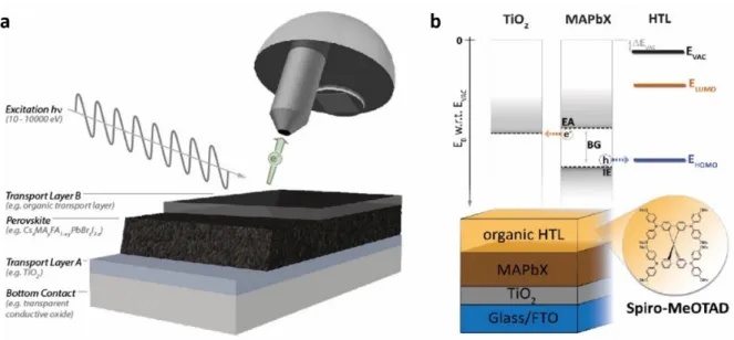
Figure 1. Photoemission spectroscopy of halide perovskite thin films. a) Schematic of the
PES experiment for a typical perovskite thin film on top of a transport layer A. For the analysis of the forming interface incremental (typically 0.1 – 30 nm) overlayers of a transport layer B can be grown on top while successively performing the PES measurements. b) Energy level diagram for a typical halide perovskite solar cell stack. PES measurements give access
to key energetic parameters, the formation of interface dipoles (Evac) and to adjacent
transport layers (here: energies of the lowest unoccupied molecular orbital, ELUMO, and
highest occupied molecular orbital, EHOMO, of an organic semiconductor).
Assuming the absence of additional chemical reactions, the determined values can be used as input parameters for transport models based on thermionic emission at HaP/metal interfaces,
i.e. in the Mott-Schottky limit,[11] or equivalently for HaP-semiconductor heterojunctions
5
by vacuum level alignment, and the interface energy barrier for electron and hole transport is the difference between the EAs and IEs of the two materials, respectively. We note that over the past decades expanded and more realistic models were developed for many semiconductor systems. Notably, the generation of these models also relied on the precise determination of the energy level alignment process between the two films and, for example, comprise interface
dipole formation and induced density of interface state effects.[13–15]
New means and increasingly powerful computational methods for the calculation of the electronic structure of semiconductor surfaces and interfaces along with more accurate PES experiments were at the forefront of the development of these models. Particularly, in situ layer
growth, to determine band onsets (i.e. the distance of the band extrema from EF) at the surface
and band offsets at the interface of two semiconductors by PES became a hallmark method for
model validation.[16]
Following this path, we will lay out how PES, as the method of choice to measure EVBM, IE and
the densities of states (DOS) of frontier electronic states at the surface, can be employed for HaP systems. We note that, in this context, often inverse photoemission spectroscopy (IPES) is
mentioned as a complementary tool to identify ECBM and the EA. For further reading on the
many interface systems that exist between HaP films and a large variety of functional layers (transparent conductive oxides, organic semiconductors, metal contacts, etc.) we point to a host of literature and review pieces that go beyond PES methods and reference further detailed
studies.[17–20]
2.Methodology
2.1. Photoemission spectroscopy: working principle and measurements conditions 2.1.1.Working principle
6
PES can be commonly considered as a set of non-destructive analytical characterization tools
based on the principle of photoelectric effect.[21,22] PES is usually performed under ultra-high
vacuum (UHV) conditions and used to determine the chemical and electronic properties of the surface and near surface region of a (semi-)conductive sample, with the probing depth depending on the photon energy used for the generation of photoelectrons. In a classical picture, the photoemission process can be described as a three-step process, occurring almost simultaneously. First, the sample is irradiated with high energy photons (either from an X-ray tube, a gas discharge lamp, laser excitation or a synchrotron radiation source), which excite electrons via the photoelectric effect. Secondly, the excited electron travels though the solid towards the surface. While on its path to the surface, the electron can be subject to multiple scattering events and hence lose parts of its initial kinetic energy, which would eventually give rise to well defined background contribution in the captured (photo)electron distribution curve
(EDC) from these so-called secondary electrons.[23–26] However, part of the excited electrons
escape the solid without energy loss through the surface into UHV and are subsequently captured and detected in the spectrometer in the final step. These primary electrons are emitted with well-defined kinetic energies, which correlate to a first approximation with the
corresponding binding energy the electrons had in their initial bound state in the solid.[27] In this
way the electron provides insight into the nature and atomic level of the material it is emitted from and yield element and compound dependent signatures in the EDC.
Mathematically, the photoemission process can be expressed according to the Equation 1:[28]
𝐸𝐾 = ℎ𝜈 − 𝐸𝑏− 𝑊 (1)
with, the measured kinetic energy EK, the photon energy hν, the binding energy the electron
had in the solid Eb, and the spectrometer work function W.
The incident photon energy determines the range of accessible binding energies of occupied states in the solid and hence the nature of the probed electronic energy levels, i.e. deep core
7
levels, shallow core levels or valence band electrons. As a final point concerning the working principle of PES, we note that the photoemission process generates, via the emission of a free electron, an atomic perturbation that is the photohole, i.e. a positive charge remaining on the surface. In a more involved theoretical description this photohole would be considered in the
final state energy of the electronic systems.[27] Practically, this perturbation must be
compensated by complex de-excitation phenomenon which needs to be considered accurately. Furthermore, as soon as the solid has poor electrical conductivity (charging) or (photo)chemical
instabilities,[29] which can be the case for complex materials such as HaPs, de-excitation and
charge compensation become a considerable challenge for the PES experiment.
2.1.2.Measurements parameters Vacuum environment
Standard PES measurements are run under UHV conditions.[29] These measurement conditions
are required since the UHV environment allows the analysis of pristine sample surfaces and for unperturbed trajectories of the photoelectrons through the spectrometer to the detector.
Thus, first UHV minimizes surface contamination of the probed sample. For reference, a perfectly clean surface (e.g. via sputter-anneal-cycles) is covered by a monolayer of CO
molecules within 1 second at a background pressure of 10-6 mbar. Second, as electrons with
low energy are easily scattered by the residual gas molecules, a good ratio between the noise
and the total spectral intensity typically requires working at a pressure in the range of 10-8 to
10-10 mbar.[30]
We note in this context that due to the recent developments in vacuum equipment and spectrometer configurations for PES experiments, it is now possible to probe surfaces under more realistic environmental conditions, i.e. at higher pressure through Near Ambient Pressure
8
phase and the surface at a pressure of up to 20 mbar, by placing a sample inside a specific cell which is opened to the analyzer via a small aperture. For HaP semiconductors dedicated experiments that probe the interaction between the HaP surface and environmental gases, such
as O2 and H2O, by NAP-XPS, can yield invaluable information on the degradation relevant in
many device applications.[32,33]
Probing depth
Generally, the probing depth in a PES experiment is limited by the escape length of the photoemitted electrons, which is related to their inelastic mean free path (IMFP) in the solid and hence the corresponding kinetic energy of the electrons. This surface selectivity is a fundamental characteristic and strength of PES techniques, but also limits their applicability for the characterization of bulk properties.
The photoelectron IMFP describes the mean distance an electron of a specific kinetic energy can travel through the solid before it scatters inelastically, thereby losing energy to its
surroundings.[34] Values for the IMFP were compiled by Seah and Dench [35] (Figure 2) and
plotted in a “universal curve” that yields an estimate for the attenuation length of photoelectrons in various PES (and IPES) techniques. The actual probing depth amounts to approximately three times the IMFP, with more than 60% of the signal coming from within a distance of one
IMFP from the surface.[29] Therefore, typically the probing depth will vary between 1 nm and
15 nm, depending on the PES technique used. It is however important to note that, in the low kinetic energy electrons range, the IMFP value is mainly dependent on the electron-phonon scattering, which will vary regarding the nature of the material. Thus, the depth analysis is
highly material dependent and can vary by an order of magnitude.[27,36–38] Today, the most
9
Figure 2. Inelastic mean free path (IMFP) of electrons in pure elemental materials as a
function of the electron kinetic energy yielding the "universal curve" according to Seah and
Dench. Adapted with permission.[35] Copyright 1979, American Chemical Society.
However, the IMFP parameter should not be the sole parameter employed for depth-resolved analysis since it only takes the effect of inelastic scattering into consideration. The implementation of the effective attenuation length (EAL), which includes the effects of both elastic and inelastic scattering, is one option to overcome this shortcoming. By including elastic scattering, the apparent depth of electrons can increase without inducing any change in energy, when layers of different electron densities are studied at off normal takeoff angles, due to modifications of the emitted angular distribution of electrons and thus, of the shape of energy
spectrum distribution curve.[34,40]
Further quantitative assessment of vertical position of atom in the analyzer area can also be achieved by considering the energy loss during PES measurements. These losses are related to two origins, firstly due to the creation of core holes, and secondly due to the transition of the
10
these aspects,[42–44] it is possible to investigate the influences of surface texturing [45] but also
vertical compositional information.[46]
2.2.Commonly Applied PES Techniques
Comprehensive descriptions and guidelines for the performance of PES measurements can be
found in literature for a broad range of material systems in general[34] and halide perovskites in
particular.[47] In this section we give a brief overview over the most common PES methods, that
found widespread applications for the determination of chemical and electronic properties at HaP surfaces and interfaces.
2.2.1.X-ray Photoelectron Spectroscopy (XPS)
Among all PES techniques, XPS is the most commonly used, and is hence sourced exhaustively
in existing reports and textbooks.[27–29,34,48] In XPS measurements, photoelectrons are excited
by an X-ray source operating at excitation energies between 150-2000 eV, i.e. in the range of soft X-rays. We will discuss hard X-ray-based PES methods that offer a larger probing depth in separate subsections (sections 2.2.2 and Erreur ! Source du renvoi introuvable.). For standard XPS measurements the typical sources available in laboratories are based on Al or Mg anodes emitting Al Kα (1486.6 eV) or Mg Kα (1256.6 eV) radiation, respectively.
For each element present in the material under investigation, one or several photopeaks at specific energy (dependent on the core level) are observed within the recorded energy range. Except for H and He, all elements from the periodic table exhibit these characteristic core level photopeaks as “finger prints” which in turn allow the assignment of atomic components of the probed surface in the XPS analysis. Moreover, and with particular relevance for multicomponent HaP systems, the evolution of the chemical environment of the observed atomic species can be determined by tracking chemical shifts in the photoelectron binding
11
For the analysis of the chemical composition, XPS serves as a quantitative tool as the photopeak intensities are proportional to the atomic concentration weighted by the energy level dependent photo-ionization cross-section . Values for are strongly depending on the kinetic energy, thus linked to the used excitation energy, but have been determined and tabulated for many core
levels under standard XPS conditions.[27,29,34] Depending on the cross-section of the most
prominent characteristic photopeak the detection limit in XPS can range down to 0.5% at.
The energy resolution of the spectra is critical for the precise determination of the electron’s EB
and is dependent on the electron energy analyzer as well as the X-ray source.[48] By using
monochromatic sources, one can obtain an energy resolution as low as 0.3 eV, providing thus a very accurate interpretation of the chemical environments in the probed region when dedicated fits to the spectra are performed. Concerning the spatial resolution, the analyzer spot size is now close to 10-30 µm for laboratory spectrometers and can reach down values within the range of micrometer (up to 1µm for Kratos instruments) for specific energy analyzer configurations.
XPS photopeaks nomenclature is based on quantum numbers and is widely documented in
literature.[27,29,34,49] With the exception of the s orbitals (angular momentum quantum number l
= 0), all orbital levels present a doublet, with a spin-orbit splitting (j = l + s), where the two
possible states exhibit a different EB for the two spin components.[49] Nowadays, spin-orbit
splittings are well tabulated in literature [29] for all element core levels, which aids significantly
for high resolution peak fitting.
2.2.2.Hard X-ray Photoemission Spectroscopy (HAXPES)
As mentioned in the preceding section, the probing depth for a classical laboratory spectrometer operated with Al or Mg X-ray source is limited to approximately 10 nm. Current trends in the
advancement of XPS methods [50] focus on the use of radiation with higher excitation energies
12
well illustrated by the universal curve for the electron IMFP and the corresponding energy range above 2 keV (Figure 2).
An initial reason to introduce HAXPES measurements has been to reduce the effect of surfaces,
i.e. contamination, and capture more signal originating from the bulk of the probed materials.[51]
In a systematic approach, the variation of the excitation energy lets us sample the composition at the surface and in the sub-surface region. For HaP films this approach is valuable as it offers insight into potential stoichiometric deviations due to the segregation of chemical species as will be discussed in section 3.4.
Hard X-rays can either be generated at synchrotron beam lines or also on a laboratory scale with the recent development of new sources. For example, by using the Ag Lα line (2984.2 eV) instead of the Al Kα (1486.6 eV), the information depth is extended to about 18 nm from the sample surface. However, sources yielding even higher photon energies (and thus extending the probing depth) become available such as X-ray anodes producing Ga Kα (9252 eV) radiation.
Generally, the type of data gained from HAXPES measurements is the same as in a regular XPS experiment, but some disadvantages amount to a loss in energy resolution as well as in the photoionization cross-section. Accurate data for photoionization cross-sections at high energy excitation are not as routinely available as for Al or Mg X-rays sources. Hence, the quantitative interpretation of core levels intensities remains ambiguous and requires careful calibration steps for new compounds and rarely probed core levels. Moreover, HAXPES techniques need to be performed with the caveat of potentially more pronounced beam damage of the samples than in soft X-ray methods. While the larger inelastic mean free path of high energy electrons implies fewer interactions with the material and thus integrally less beam damage, the potential for sample degradation is rather rooted in the nature of the typical radiation flux. HAXPES measurements are usually performed at synchrotron light sources, which exhibit a higher
13
brightness compared to laboratory-based X-ray sources. In order to achieve similar signal to noise ratios, spectrum acquisition is usually done with high X-ray flux in the analyzer spot. It is thus important to perform measurements with intensities which will not lead to a faster chemical degradation of HaPs (Pb0 growth for example) due to their high sensitivity (especially
the photosensitivity).[52] Means to follow these precautions are to de-tune the monochromator
of the incoming X-ray beam or use filters to attenuate the beam intensity particularly for lower order reflections in the range of soft X-ray which would otherwise accelerate sample degradation. Several examples show that HaP film formulations exist, that can provide high
stability even under an excitation energy of 2100 eV.[53]
2.2.3.Ultraviolet Photoemission Spectroscopy (UPS)
In UPS measurements, samples are irradiated with ultraviolet photons, either from a discharge lamp (most commonly He I or He II emission at 21.2 or 40.8 eV, respectively) or by laser excitation or in the distant UV by synchrotron radiation. Analogous to the process in XPS measurements, the UV-excited photoelectrons are then collected to retrieve the EDC and hence
the density of states.[48]
In practice, the energy resolution of the UPS experiment is on the order of 0.1 eV but can be as high as only a few meV in dedicated setups with highly monochromatic sources and low temperature conditions. This allows for a more precise determination of the valence band density of states, including the electronic states near the Fermi level. The spatial resolution is strongly dependent on the electron analyzer and photon source used, but can go down to 10
µm.[48] For the most common UPS measurement procedure using He I excitation (21.22 eV),
the kinetic energy of electrons originating from the valence band onset and frontier occupied molecular orbitals is on the order of 15-20 eV. This principally makes standard UPS measurements more surface sensitive than their XPS counterparts, restricting analysis to the
14
very top layers of the studied surface. Thus, the avoidance of surface contamination becomes critical for an accurate characterization of the valence band features by UPS.
2.2.4.Inverse Photoemission Spectroscopy (IPES)
IPES is a surface sensitive method that is complementary to the PES tool box. In contrast to PES measurement, in IPES the sample is irradiated with low kinetic energy (5 – 50 eV) electrons. After entering the solid, the electrons dissipate their kinetic energy, either radiatively or non-radiatively, and reach states at lower energy. If this decay is radiative, the emitted photon
can be detected.[54] As the initial energy of the electron is known, the measured energy of the
emitted photon leads to the determination of the final state, which represents a previously
unoccupied energy level above the Fermi level.[55] Thus, this spectroscopy technique unlocks
access to the unoccupied density of states from the conduction band.[27]
Acquisition times in IPES measurements are longer than the UPS ones, due to a significantly lower count rate. The energy resolution can reach ∼0.2 eV with a spatial resolution of around
1 mm.[55]
2.2.5.Angle-Resolved Photoemission Spectroscopy (ARPES)
For all PES measurements presented above, the photoemission is generally detected along the normal of the sample surface and via angle-integrating electron optics. The basic principle of ARPES is to vary the observed emission angle of electrons, either by tilting the sample, by moving the analyzer, or in a specific analyzer and detector configuration (p-ARXPS) , which is based on the simultaneous collection of the photoelectrons emitted under different angles
without tilting the sample.[56]
Furthermore, area detectors enable the discrimination of emission angles for electrons within the acceptance cone passing through the analyzer optics.
15
By introducing angular resolution in XPS measurements, quantitative information about the depth distribution of the elements in the top few nanometers of the sample can be extracted, as one can reduces the effective escape depth of electron at emission under grazing angles. Performing HARPES (Hard X-ray Angle-Resolved Photoelectron Spectroscopy) presents a versatile approach to vary the surface contribution to the spectrum and obtain a more discriminate picture of the bulk and surface electronic structure and chemical composition. Finally, angle-resolved UPS (ARUPS) measurements consist of acquiring several spectra at varied angles from a monocrystalline or highly ordered polycrystalline material, which leads to the generation of “band-maps” of the electronic structure of the valence bands, i.e. mapping of
the dispersion relation.[48] Note that this analysis can also be pursued at higher photon energies,
by working with hard X-ray excitation in HARPES mode. This provides a more bulk-sensitive electronic structure determination through angle-resolved band mapping, particularly attractive for ex-situ prepared samples, with surface contamination. It is however necessary to keep in mind that working in the hard X-ray regime can lead to specific issues, such as increased
radiation damage.[57]
Clearly, coupling all these PES techniques is thus a comprehensive approach to obtain a complete overview of the chemical and electronic properties of materials. Hence, the surface chemical gradient inside the top material layer and its quantification can be easily determined at different probed thicknesses through a combined study with XPS, ARXPS and HAXPES measurements and will be detailed in section Erreur ! Source du renvoi introuvable.. with specific application to HaP materials.
2.3.Spectrometer calibration and the influence of charging effects
Recently, the issue of faulty data analysis in PES measurements has been raised by the research
community, which highlights poor and incorrect material data analysis in the past.[58] The aim
16
measurement, for which we rather refer to existing ASTM standards,[59–62] ISO standards[63–65]
and additional literature,[34,66] especially for HaPs materials.[38,47] More specifically, Philippe et
al.[38] recently detailed good practices regarding PES measurements for HaPs (sample
preparation, calibration, radiation damages).
However, we would like to emphasize the question of charging effects during PES measurements since they can lead to important misinterpretations of PES data. We thus turn to a technical aspect that can become particularly relevant for the determination of the binding energy of core levels. In case of poorly conductive samples, which holds true for a subset of HaP compounds in the absence of photogenerated carriers over the entire sample structure, one can encounter erroneous photopeak positions due to charging. This charging effect is corresponding to photoholes that accumulate at the sample surface leading to a positive electrostatic potential. In consequence, photoelectrons leave the sample at lower kinetic energies. During XPS measurements, this charging effect hence leads to an apparent shift of the photopeaks to higher binding energies. Thus, charge compensation can become necessary for measurements in which electrostatic charging occurs. Usually charge compensation can be achieved by “flooding” the sample surface with an excess of low-energy electrons to balance
out the positive charges.[29] This workaround enables that an elemental quantification can still
be obtained in the case charge compensation is used for the measurement. Other methods are
also available from literature, with specific focus on sample mounting.[34] However, we note
that the identification of chemical environments becomes more difficult and needs to strongly rely on the analysis of core level peak positions relative to each other at best. In addition, the determination of band onsets is no longer possible, as the constant flow of electrons constitutes
an arbitrary shift of EF on the sample surface.
When reaching the determination of energetic diagrams, issues raised by the charging artefact become more critical. Indeed, in this case; charge compensation via flooding is not appropriate.
17
To overcome this issue, the sample preparation as well as calibration step (especially for UPS
measurements) are key parameters and some examples can be found in literature.[34,38] It is also
very important to corroborate the experimental data obtained through PES measurements with other experimental work to probe the validity of the energetic diagrams obtained. More details will be specified in Section 3.2.
3.PES analysis of HaP material properties
3.1.Stoichiometry and chemical composition
The stoichiometry measure by XPS is highly dependent on the chemical environment at the HaP surface, but the accuracy of the evaluation can be improved by an appropriate choice of
photopeaks and the corresponding range of EB. Indeed, the probing depth of the analysis varies
depending on the chosen energy range. This effect is typical for system in which the surface composition deviates from the bulk composition and was for instance reported for other materials that find application in photovoltaic and other optoelectronic applications. For
example, in the case of Cu(In,Ga)Se2 solar absorber layers, the GGI key ratio ([Ga]/([Ga]+[In]))
evolves from 0.25 to 0.29 depending on the energy range chosen for the photopeak analysis
(EK = 675 eV if Ga 2p3/2 and In 3d5/2 levels are chosen and 10 eV if the Ga 3d and In 4d levels
are chosen for the analysis, respectively), for a theoretical value of 0.30.[67] The larger the
distance between the binding energy range of two or more probed elements, the larger is the variation in IMFP, which poses a predicament on the determination of the absolute stoichiometry.
The issue can be rectified by applying a kinetic energy dependent sampling depth correction, which however does not eliminate surface segregation or gradient effects. However, it is not always possible to access core levels with neighboring energy ranges for materials with complex stoichiometries such as HaPs. Indeed, as described in the following paragraph, wide
18
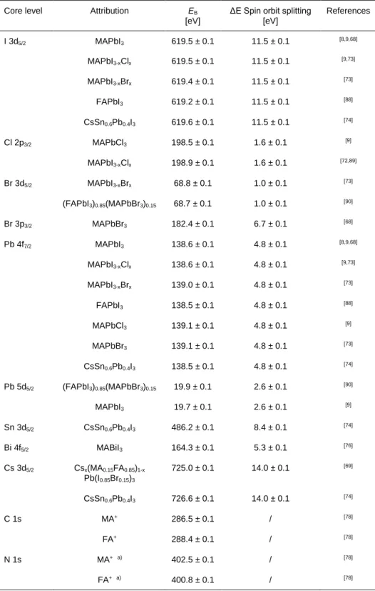
energy windows are involved for HaP materials, with at least an energy difference of 250 eV between the nitrogen and iodine core levels. Therefore, as there is a lack of better alternatives, recording the major photopeaks of the constituent elements, for which standard spectra are indexed in the literature, is the more advised strategy. In the following we give a few select examples of the most relevant elements probed for HaP analysis.
Multiple halide elements can be implemented for HaPs solar cells, the most common ones being
I, Br and Cl. Numerous comparative studies of MAPbX3 (where X represents the halide)
absorbers can be found in literature,[8,9,68–70] enabling a more consistent indexation of the BE
peak positions of the main core levels: I 3d5/2 (619.5 ± 0.1 eV), Cl 2p3/2 (198.5 ± 0.1 eV) and
Br 3d5/2 ( 68.5 ± 0.2 eV). Those EB can slightly evolve, especially for mixed cations such as
MAPbI3-xClx and MAPbI3-xBrx (Table 1).[71–73]
The case of Pb is interesting because the corresponding EB will be influenced by the halide
element it is bound to. Indeed, for MAPbI3 system, the Pb 4f7/2 photopeak is positioned at a EB
of 138.6 ± 0.1 eV but is shifted to 139.1 ± 0.1 eV in pure MAPbCl3 or MAPbBr3 structures.[9,68]
For MAPbI3 systems the binding energy range from 15 to 55 eV is suitable for a more accurate
chemical analysis as it contains the Pb 5d and I 4d core levels (Pb 5d5/2 at 19.7 ± 0.1 eV and I
4d5/2 at 49.5 ± 0.1 eV), offering measurements at similar probing depth for both elements.[9]
In this context we note that lead can be substituted with tin. Liu et al.[74] studied the
incorporation of Sn in mixed perovskites with different structures. For CsSn0.6Pb0.4I3
quantum-dots, they found the Sn 3d5/2 EB at 486.2 ± 0.1 eV. Kamarudin et al.[75] found that several
oxidations states are attainable for Sn, with Sn4+ at 486.9 ± 0.1 eV, Sn2+ at 485.9± 0.1 eV and
Sn0 at 484.5± 0.1 eV in EB for FA0.98EDA0.01SnI3 structures. Furthermore, heterovalent
substitutions of lead are attempted, for instance by Bi, to expand the class of perovskite-like
materials.[76] The binding energy of the Bi 4f7/2 photopeak in (CH3NH3)3Bi2I9 is located at 159.0
19
(159.4± 0.1 eV and 159.0 ± 0.1 eV, respectively), the best reference to index to MABiI3 position
becomes thus Bi 4f5/2, located at 164.3 ± 0.1 eV (spin orbit splitting of 5.3 eV).
For more complex structures such as triple cation mixed halide perovskites (Cs0.05(MA0.15FA0.85)0.95Pb(I0.85Br0.15)3 and Cs0.1(MA0.15FA0.85)0.9Pb(I0.85Br0.15)3 for example),
where FA denotes organic formamidinium (C(NH2)2) cations, the literature remains sparse. For
reference, the Cs 3d5/2 core level in this structure is located at 725 ± 0.1 eV.[69] This position
slightly shifts for a different perovskite structure such as CsSn0.6Pb0.4I3 quantum-dots where it
is measured at 726.6 ± 0.1 eV, even though the Pb 4f7/2 and I 3d5/2 peak positions are found at
their usual binding energy (138.5 ± 0.1 eV and 619.6 ± 0.3 eV respectively).[74]
Fitting the C 1s spectrum is complex and is ideally performed in correlation with the N 1s
spectra fitting. Indeed, one would only expect the presence of C-N bonds, in MA+ and/or FA+,
which have been well identified.[77,78] Jacobsson et al.[78] performed the deconvolution of the C
1s and N 1s spectra based on three different perovskites, using MAPbBr3, FAPbI3 and mixed
perovskite (FAPbI3)0.85(MaPbBr3)0.15 (obtained by spin-coating). Specific EB values for the C
1s were derived from their work, namely at 288.4 and 286.5 eV for the carbon in FA+ and MA+,
respectively; the corresponding N 1s positions were determined at 400.8 and 402.5 eV, respectively, but were shifted by +0.2 eV in the case of mixed halide perovskite (Figure 3, a
and b). Table 1 summarizes values for EB and spin orbit splitting for the major core levels
photopeaks of HaP materials.
Often, other contributions at lower EB - between 285.4 eV and 284.6 eV - are observed in the
C 1s region and have to be indexed according to their EB. Jung et al.[77] attributed a contribution
in this region to the presence of CH3-NH2 at 285.4 eV, in correlation with literature values.[79]
They found this component for HaP films that were grown via two different deposition
20
a sequential vacuum evaporation process.[80] They assume this carbon contribution to be a
structural defect at the interface between MAI and PbI2, which disappeared after annealing.
Another C 1s photopeak observed at 285.3 eV was attributed to the presence of CH3I [81] which
could arise from the thermal decomposition of MAI (Figure 3, c-e).[82] In addition, adventitious
carbon can be present when films have been exposed to ambient or other environmental conditions that lead to inherent contamination. In this case, multiple additional components can be detected on the surface: C-C bond at 284.5 to 285 eV (depending on the initial calibration
performed) due to the presence of hydrocarbons species in air,[83] but also oxygen-related
species, for which carbon-oxygen bonds (i.e. C-O, C=O, C-OH, RCOOH…) yield signal in the
energy range between 285.5 and 289 eV.[84,85] For the latter, the corresponding O contamination
becomes also apparent by the detection of the O 1s core level at EB of 532.3-532.8 eV.
Attribution of the contribution of C 1s at low EB is thus not always well-defined, and has to be
performed with precautions.[82,86] In this context we note that the calibration of binding energy
scale to adventitious carbon has been a subject of controversial discussion, as it grossly neglects
insufficient Fermi level alignment between spectrometer and the probed sample surface.[87]
Now, particularly in the case of hybrid HaP materials and the corresponding multi-component carbon signal, we highly discourage the use of this referencing method.
21
Figure 3. a) and b) N 1s and C 1s core level spectra (respectively) of the
(FAPbI3)0.85(MaPbBr3)0.15, FAPbI3 and MAPbBr3 deposited on amorphous SnO2/FTO
substrates. Reproduced with permission.[78] Copyright 2016, American Chemical Society. c),
d) and e) Pb 4f, I 3d and C 1s core level XPS spectra (respectively) of the MAPbI3 film (i) and
the samples after depositing an additional excess MAI layer of 1 (ii), 2 (iii), 4 (iv), 8 (v), 16
(vi), and 32 nm (vii). Reproduced with permission.[82] Copyright 2017, American Chemical
22
Table 1. Characteristics of the main core level photopeaks of HaPs: EB (eV) and spin orbit
splitting (eV).
Core level Attribution EB [eV]
ΔE Spin orbit splitting [eV] References I 3d5/2 MAPbI3 619.5 ± 0.1 11.5 ± 0.1 [8,9,68] MAPbI3-xClx 619.5 ± 0.1 11.5 ± 0.1 [9,73] MAPbI3-xBrx 619.4 ± 0.1 11.5 ± 0.1 [73] FAPbI3 619.2 ± 0.1 11.5 ± 0.1 [88] CsSn0.6Pb0.4I3 619.6 ± 0.1 11.5 ± 0.1 [74] Cl 2p3/2 MAPbCl3 198.5 ± 0.1 1.6 ± 0.1 [9] MAPbI3-xClx 198.9 ± 0.1 1.6 ± 0.1 [72,89] Br 3d5/2 MAPbI3-xBrx 68.8 ± 0.1 1.0 ± 0.1 [73] (FAPbI3)0.85(MAPbBr3)0.15 68.7 ± 0.1 1.0 ± 0.1 [90] Br 3p3/2 MAPbBr3 182.4 ± 0.1 6.7 ± 0.1 [68] Pb 4f7/2 MAPbI3 138.6 ± 0.1 4.8 ± 0.1 [8,9,68] MAPbI3-xClx 138.6 ± 0.1 4.8 ± 0.1 [9,73] MAPbI3-xBrx 139.0 ± 0.1 4.8 ± 0.1 [73] FAPbI3 138.5 ± 0.1 4.8 ± 0.1 [88] MAPbCl3 139.1 ± 0.1 4.8 ± 0.1 [9] MAPbBr3 139.1 ± 0.1 4.8 ± 0.1 [73] CsSn0.6Pb0.4I3 138.5 ± 0.1 4.8 ± 0.1 [74] Pb 5d5/2 (FAPbI3)0.85(MAPbBr3)0.15 19.9 ± 0.1 2.6 ± 0.1 [90] MAPbI3 19.7 ± 0.1 2.6 ± 0.1 [9] Sn 3d5/2 CsSn0.6Pb0.4I3 486.2 ± 0.1 8.4 ± 0.1 [74] Bi 4f5/2 MABiI3 164.3 ± 0.1 5.3 ± 0.1 [76] Cs 3d5/2 Csx(MA0.15FA0.85)1-x Pb(I0.85Br0.15)3 725.0 ± 0.1 14.0 ± 0.1 [69] CsSn0.6Pb0.4I3 726.6 ± 0.1 14.0 ± 0.1 [74] C 1s MA+ 286.5 ± 0.1 / [78] FA+ 288.4 ± 0.1 / [78] N 1s MA+ a) 402.5 ± 0.1 / [78] FA+ a) 400.8 ± 0.1 / [78]
a)(Positions are shifted by +0.2 eV in the case of mixed halide perovskite)
23
As laid out in the introduction, PES gives access not only to the chemical but also to the electronic properties of a material. Before describing the detailed process of characterizing the electronic properties, and thus the energy level alignment (ELA) at the interface, we briefly recap some important parameter definitions concerning the electronic properties of a surface that had been introduced earlier.
The first two important reference energies necessary to assess the position of electronic levels
are the Fermi level (EF) and the vacuum level (EVAC), which were introduced earlier. EF
represents the energy at which the probability of occupation of an electronic state is ½ and is hence inherently linked to the electronic structure and electrochemical potential of the material
investigated. For metals, EF cuts through the conduction band and marks the limit between
occupied and unoccupied states, while for an intrinsic or non-degenerately doped
semiconductor, EF is located within the band gap. EVAC represents the energy threshold an
electron needs to overcome in order to escape from the solid into vacuum. The work function (WF) represents thus the difference between those two values, according to the Equation 2:
𝑊𝐹 = 𝐸𝑉𝐴𝐶 − 𝐸𝐹 (2)
Similarly important are the distance between VBM and EF as well as the distance between CBM
and EF, defined as the onset energies, EVBM and ECBM, respectively. These quantities are linked
to the position of the Fermi level in the gap and hence the doping of the probed surface. They are directly related to IE and EA by the following equations 3 and 4:
𝐸𝑉𝐵𝑀 = 𝐼𝐸 − 𝑊𝐹 (3)
𝐸𝐶𝐵𝑀 = 𝑊𝐹 − 𝐸𝐴 (4)
A thorough investigation of these electronic properties to study the ELA in complex heterostructures can be achieved by a combination of XPS (position of the valence band
24
band region, work function),[92] and IPES (position of the conduction band onset relative the
Fermi level)[54] measurements.
It is important to note that the values obtained through PES measurements should always be compared to other experiments in order to validate the absence of any charging effect. Optical measurements as well as theoretical band gap predictions can be a good lead to compare the
data obtained,[93,94] as well as a more recently developed technique named chemically resolved
electrical measurements (CREM), developed by Cohen and coworkers.[95,96] For CREM,
charging effects are consistently being followed and subsequently accounted for, to allow for the construction of a realistic band diagram for multi-interfacial structures. Another promising approach is the performance of operando PES measurements, which has been successfully
demonstrated by Teeter et al.[97] for chalcopyrite solar cells. The authors find that
photoexcitation due to x-rays or stray visible light during XPS or similar measurements can produce measurable photovoltages in materials, and thus, improve band-offset determinations with more reliable values for the junction built-in voltage.
A first complete description of the ELA in HaPs solar cells as measured by a combined PES/IPES approach was reported by Schulz et al., in conventional as well as inverted device
geometry.[10,98] Since then, the community explored more meticulously the electronic properties
in general, and the band edge determination leading to the correct energy level assessment by
PES/IPES in particular, which is topic of several reviews.[6,20,99,100] Note that the choice of the
PES method employed can be critical when evaluating the intrinsic electronic properties of the perovskite surface. When perovskite films have been exposed to ambient air, the determining
EVBM by XPS is more precise than by UPS,[101] as UPS is more surface-sensitive and thus, more
susceptible to inherent contamination. Apart from the ELA assessment, more recently complete
band structure measurements of single crystalline HaPs were obtained, for MAPbI3 and
25
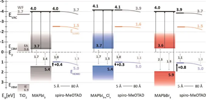
Looking back at typical values of ELA in HaPs, we begin with the study by Schulz et al.,[98] in
which they investigated films with different compositions and provided first complete energy
level positions for MAPbX3 films (X = I, Br, I3-xClx) on top of TiO2 bottom layers with and
without thin evaporated HTLs as overlayer. Through the combination of UPS and IPES
measurements, they obtained WFs of 4.0 eV for MAPbI3 and MAPbBr3 and 4.1 eV for MAPbI
3-xClx, IEs of 5.4 eV for MAPbI3 and MAPbI3-xClx and 5.9 eV for MAPbBr3, EAs of 3.7 eV for
MAPbI3 and MAPbI3-xClx and 3.6 eV for MAPbBr3 and electronic gaps of 1.7 eV for MAPbI3
and MAPbI3-xClx and 2.3 eV for MAPbBr3 (Figure 4). The electronic gap values from combined
UPS and IPES were assessed by comparison with optical measurements and density functional theory (DFT) calculations including spin-orbit coupling and GW approximation. Hence, the absence of charging allowed for an accurate determination of the band onsets for the study
performed by Schulz et al.[98]
In order to assess the ELA to an adjacent HTL, the corresponding organic semiconductor is deposited on top in incremental steps, leading to a gradual buildup of the interface. This
procedure has been pursued for the commonly employed HTL material
N2,N2,N2′,N2′,N7,N7,N7′,N7′-octakis(4-methoxyphenyl)-9,9′-spirobi[9H-fluorene]-2,2′,7,7′-tetramine (spiro-MeOTAD) in the study by Schulz. The measurements indicate that vacuum level alignment occurs at this particular interface between HaP and
spiro-MeOTAD, leading to an apparent offset between EVBM in the HaP and the EHOMO of the
spiro-MeOTAD layer, which does not cause a barrier for hole extraction from the HaP to the HTL, but could in principle pose a limit to the attainable photovoltage. This initial PES investigation of this interface system led to further studies which indicate that the valence band offset in the ELA has no major impact on the device performance as long as the IE of the HTL is smaller
than the IE of the HaP film.[6,107,108] Endres and co-workers [109] also performed similar
26
combined the approach with a density functional theory (DFT)-based theoretical calculation of
the DOS. In that work they corroborated the values obtained by Schulz et al.[98] for MAPbI3
and MAPbBr3 by a refined fitting procedure for the band edges (see section 4.2).
Figure 4. Experimentally determined energy level diagrams of interfaces between
spiro-MeOTAD and MAPbX (X = I3, I3-xClx, Br3) on TiO2. Each diagram provides the perovskite
band gap, Fermi level position, electron affinity, ionization energy and work function. The HTL HOMO and LUMO positions with respect to the perovskite VBM and CBM underline key points of hole extraction and electron blocking, respectively. Minor band bending is observed
throughout the spiro-MeOTAD film. Reproduced with permission.[98] Copyright 2014, Royal
Society of Chemistry.
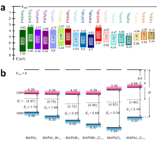
Recently, Olthof and her co-workers [110] performed a systematic study of the energy level
positions in tin- and lead-based HaPs, by exploring the electronic properties of 18 different
AMX3 perovskite structures, through the variation of monovalent cations (A = FA+, MA+ or
27
a better understanding of the changes in the band gaps as well as the influence of composition on the absolute positions of VBM and CBM as measured by PES/IPES. The findings consistently track the increase in band gap energy with changing halide species, going from I to Br to Cl, in accordance with optical measurement and ab-initio calculations. Hence, CBM energy is shifted upward while a downward shift is observed for the VBM; both shifts correlate with the electronegativity and the metal to halide bond distances decrease (again from I to Br to Cl in decreasing order). The IEs and EAs of Sn-based perovskites are lower than those of their Pb-based counterparts, which is attributed to the lower electronegativity of Sn compared to Pb. As for the monovalent A-site cation, Olthof et al. report on a more convoluted trend in the change of the absolute IE and EA values, which they ascribe to a subtle interplay of the structural parameters on the unit cell scale (Figure 5, a).
Mixed halide perovskites also present an interesting trend in the electronic structure with regard
to their single halide perovskite counterparts, as measured by PES. Li et al.[111] studied the
influence of the halide nature, by tuning its composition in MAPbX3 (MAPbCl3, MAPbBr3,
MAPbI3, MAPbBr1.5Cl1.5, MAPbI2.1Br0.9 and MAPbI2.1Cl0.9). The partial substitution of I by Br
or Cl (MAPbI2.1Br0.9 and MAPbI2.1Cl0.9)leads to a fine control of the electronic properties,
characterized by intermediate band onsets between those of the single halide perovskites (Figure 5, b). These dedicated PES/IPES studies are a first important step towards compiling a library of energy levels and have to be extended to other mixed HaPs.
28
Figure 5. a) Schematic energy level diagram of 18 HaPs, with variations of monovalent cations,
metal cations and halide anions with the respective IE, EA and band gap values. Reproduced
with permission.[110] Copyright 2019, Springer Nature. b) Schematic energy level diagram of
six metal halide perovskites, with variations of halide anions with the respective IE, EA and
band gap values. Reproduced with permission.[111] Copyright 2016, American Chemical
Society.
3.3.Reproducibility and reliability
Various deposition techniques for HaP thin film formation [4,81,112–120] as well as a variety of
device architectures, i.e. conventional [100,121–124] or inverted [125–131] devices with a diverse
selection of electron transport layer (ETL) or hole transport layer (HTL) have been realized to optimize device performances. It is noteworthy that the various deposition techniques and different sample architectures of HaP thin films induce a substantial variability of the PES
29
results for stoichiometric quantification and electronic properties. As an example, in literature,
the electronic parameters values of MAPbI3 vary significantly, with, for example, IE values
ranging from 5.1 to 6.6 eV.[98,101,132–137]
3.3.1.Preparation method
Wang et al.[138] studied the effect of five different deposition techniques on the surface
composition of MAPbI3 deposited on Si substrates by XPS. They showed that the composition
varies from one deposition technique to another, mainly in the carbon content, and related these
variations to the dissociation of MAPbI3 during the film formation.
Emara et al.[139] tried to correlate the electronic properties of MAPbI3 films with the device
efficiency of corresponding perovskite solar cells. They performed a UPS study on 40 MAPbI3
films prepared with various methods and concluded that varying the preparation conditions leads to a wide range of electronic properties as the IE values were scattered within a range of 0.8 eV, which they attribute to fluctuations in the Pb/N ratio.
In a similar study, Wang et al.[138] report on a dependence of the work function on the deposition
method, yet the spread in observed IEs is less pronounced than in the study of Emara et al.[139]
Note that, for both studies, the evolution of electronic structure and properties is correlated with the evolution of the surface stoichiometry (assessed by XPS). These examples demonstrate that PES is a powerful tool to correlate surface composition and energetics of HaPs. They also tell a cautionary tale that one needs to expect high sample-to-sample variance and ambiguity in the measured surface electronic properties, that can depend on minutia in the sample production process and despite other metrics (e.g. corresponding device characteristics) remaining mostly unaffected.
Sun et al.[140] used XPS mapping for laterally resolved chemical analysis of MAPbI3 thin films
to probe the influence of sample preparation parameters. They studied three different deposition
30
Imaging XPS techniques are of primary interest to investigate the surface homogeneity.[143] The
main challenge is to combine sufficient data collection in a limited amount of acquisition time
[144] with the minimization beam damage to the HaP layers. Here, Sun et al.[140] demonstrate
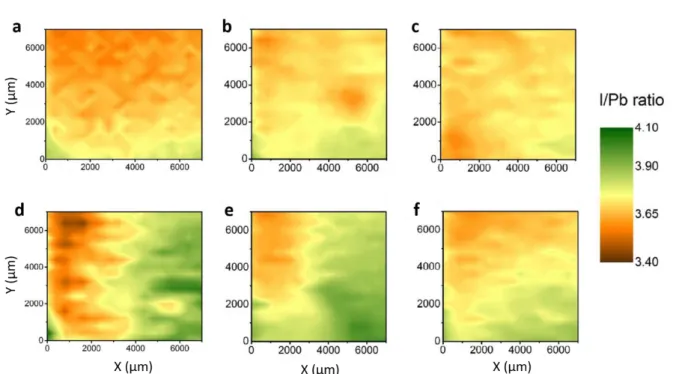
that the I/Pb ratio is not homogenous within the deposition method but also from one batch to another as well as within the same sample (Figure 6).
The work denotes a proof of concept regarding mapping of perovskite layers but reveals two critical challenges in the data analysis and correlation. The first issue is related to the discrepancy of the I/Pb ratio compared to expectation and literature values. Indeed, Sun et
al.[140] present ratios within the range of 3.1 up to 4.1, not representative of a MAPbI3 surface.
It could be explained by an excess of MAI component since, as it will be detailed in Section 4.1.2, during storage under UHV, the I/Pb values decreases due to a loss of MAI surface adsorbents. The second issue concerns the origin of the lateral segregation within a similar sample. The strong variations in the I/Pb ratio can be induced by non-uniform coverage of surface contaminating species. Indeed, as no specific information is provided for the surface composition except the evolution of I/Pb ratio, it is reasonable to imagine that contamination could also be responsible, as well as the different options offered by the authors (concentration of solvent vapor, annealing temperature…). A critical cross-examination of this hypothesis would require at least the elemental maps of C, N and O species.
31
Figure 6. Homogeneous (a, b and c) and inhomogeneous (d, e and f) I/Pb maps of MAPbI3
films deposited by different techniques according to Zhang’s procedure (a, d)[142], Ahn’s
procedure (b, e)[117] and Jeon’s procedure (c, f)[141]. Adapted with permission.[140] Copyright
2018, American Chemical Society.
3.3.2.Substrate influence
Further variations in the obtained PES results can be linked to the influence of the substrate, the
HaP film is grown upon. Olthof and Meerholz [86] addressed the influence of the substrate type
by depositing MAPbI3 following a co-evaporation process on four different substrates: Indium
doped tin oxide (ITO), MoO3, PEDOT PSS (poly(3,4-ethylenedioxythiophene) polystyrene
sulfonate)) and polyethylene ethoxylate (PEIE). After a thickness of over 30 nm has been
deposited, all MAPbI3 samples presented similar surface composition as determined in PES
measurements. However, below a thickness of 30 nm, the surface composition and the growth
mechanism appeared to be strongly substrate-dependent, with the formation of a PbI2-rich phase
32
Most importantly, the influence of the substrate can result in a significant change in the electronic properties of the HaP surface even at several hundreds of nanometers distance from
the buried interface. By exploring different n-type substrates (TiO2, ZnO, ZrO2, and F:SnO2
(FTO)) and p-type substrates (PEDOT:PSS, NiO and Cu2O), Miller and co-authors [101] found
that the substrate types apparently change the electronic properties of thin MAPbI3 layers,
specifically their doping type. This trend was confirmed by Schulz et al.[10] who investigated
several 100 nm’s thick layers of MAPbI3 on NiO and TiO2 substrates and highlighted a work
function shift of 700 meV, along with shifts of all the energy levels, depending on the substrate. This substrate dependency of the electronic properties of HaPs is further discussed in section 4.3, where we contrast the effect to potentially related phenomena such as Fermi level pinning and band bending.
3.4.Ageing and degradation
3.4.1.Modifications due to photon irradiation
The characterization of perovskites by PES, as well as their actual operation as light-harvesters in photovoltaic devices, obviously involves the exposure to electromagnetic radiation. It has been recently reported that surface photovoltage (SPV) of up to 0.7 eV can develop in an HaP film by varying the exciting UV photon flux during the UPS experiment in standard laboratory
conditions.[145] The photovoltage buildup is related to the creation of electron-hole pairs upon
UV excitation, which can substantially compensate the band bending at the surface of the
perovskite films. Such an effect is critical to the measured EB and should be considered when
assessing PES results.
The effect of actual operating conditions on perovskite films embedded in a solar cell
configuration was analyzed by XPS in vacuum.[146] The perovskite layer did not exhibit any
33
additional illumination. However, exposure to additional white light led to degradation,
characterized by the formation of metallic lead (Pb0), as also highlighted in several PES studies
on halide-based perovskites.[90,147,148] Indeed, the degradation of lead-iodide based perovskite
has been proposed to involve the formation of PbI2 and the segregation of the latter into metallic
lead and I2 by photolysis,[149,150] while a more intricate pathway for Pb0 formation is linked to a
Lewis acid base reaction centered on the de-protonation of the (organic) cation on the perovskite
A-site.[151,152] This process is further described in section 4.1.1. Interestingly, this degradation
into Pb0 appeared to be strongly constrained upon the application of a voltage bias.[146] Thus
implying that HaPs are more stable under voltage application, which could, for instance, suppress electrochemical processes.
However, a further study reports on a significant change in composition to readily occur upon
X-ray exposure.[8] At an early stage of the exposure and up to 4.5 h of exposure, this change is
characterized by the generation of iodine (I) and methyl ammonium (MA) vacancies, VI and
VMA, respectively. Steirer et al. assume that these vacancies act as self-compensating defects
that compensate each other and thus do not affect the position of valence and core levels yet. This could thus reflect on the proposed defect tolerance of perovskites at earlier stage of
irradiation and explain the negligible X-ray beam damage assessed from XPS studies.[32]
Nevertheless, over several hours of X-ray exposure the surface composition changes, with loss
of methyl ammonium and iodine , corresponding to the degradation of MAPbI3 into PbI2.[8] In
a comparable study, overnight exposure to X-rays in UHV of MAPbI3 perovskite resulted in
the degradation of MAPbI3 to PbI2 and Pb0.[153] It is noteworthy that the light-induced
degradation is insignificant in nitrogen-filled environment and mostly occurs when performing the illumination under vacuum conditions or in environments with oxygen content as low as 1 %.[148,154]
34
In summary, light and radiation exposure can damage the HaP film and even more so its surface, particularly under vacuum conditions. This (beam)damage effect can severely affect the results obtained in the XPS experiment and hence requires a careful measurement approach. Ideally spectra are recorded over short acquisition times and at reduced beam intensities to dynamically track changes that can occur during the measurement. To date the actual radiation impact or energy flux on the analyzed spot on the sample is rarely mentioned in the literature reports. Given the strong variation in HaP film stability, this induces another parameter of uncertainty in the comparison of completed studies. As a measure of best practice the radiation impact on the sample as well as transient behavior in the PES data should be reported similar to the
procedures presented above.[8,147]
3.4.2.Thermal degradation
Since several heating steps (annealing step, module encapsulation…)[155] can be necessary for
the fabrication of the HaP-based optoelectronic devices, understanding thermal degradation is thus of paramount importance and can be aided by dedicated PES experiments.
Investigations about thermal stability were performed by several groups, mostly on MAPbI3
-based samples.[156,157] For this compound, the chemical changes induced by thermal stress
appeared at a nominal temperature of 130°C, through the decrease of the N 1s and the I 3d XPS
signals, and in some cases, the growth of Pb0 signal. The study explains this evolution by the
MAPbI3 decomposition into CH3I, NH3 and PbI2, with the evaporation of CH3I and NH3 while
PbI2 remains on the surface. This thermal degradation process was claimed to progressively
occur from the film surface to its bulk, already occurring when the material was exposed to
80 °C for extended time (>60 min).[157]
Very few literature reports exist about the deviation of electronic properties due to thermal
degradation. Foley and co-authors [158] studied the evolution of MAPbI3 electronic structure
35
measured work function but observed a reversible shift in the VBM onset. In their review, Wang
et al.[138] proposed a specific mechanism that would pertain to a potential evolution of the ELA.
The model is based on an increase of PbI2 degradation product, which presents different
electronic properties compared to MAPbI3 (IE of ≈ 6.3 eV and ≈ 5.3 eV for PbI2 and MAPbI3,
respectively).
Note that combining thermal degradation and X-ray exposure during heating has also been
reported to additionally contribute to the generation of Pb0.[9]
3.4.3. Interfacial degradation
The long term stability of HaP devices is strongly related to interfaces,[6] where many different
reactions can occur, leading to degradation of perovskite absorber and thus, to the change of its electronic and optoelectronic properties. A particularly unstable interface is the metal/HaP junction. In the classical device, perovskites films are often separated from any metal cell terminal through buffer and transport layers and are hence not directly in contact with the
metallic species. However, different processes [6] can lead to the creation of metal HaP
interfaces, notably metal migration from the contacts through the transport layer directly to the
perovskite films,[159] pinholes formation inside the transport layer or more directly, via a
deliberate cell design (HTM-free PSC).[160,161]
The presence of such an interface can lead to major implications for the HaP chemical state as
proved by Zhao et al.[162] When exposed to different metals, they report the MAPbI3 surface to
spontaneously degrade through either redox chemistry reactions (Al, Ag, Cr and Yb) or partial
charge transfer (Au). They evidenced this degradation through the appearance of a Pb0
photopeak at 136.5 eV, without the presence of oxygen or light. This degradation is not specific
to hybrid perovskites since degradation is also present for inorganic perovskites such as CsPbI3
36
Liu et al.[132] monitored the evolution of MAPbI3 electronic properties by UPS upon incremental
deposition of Au on top of MAPbI3. After the first 0.5 Å Au deposition, a vacuum level shift of
0.3 eV (from 4.7 eV for pristine MAPbI3 to 4.4 eV with 0.5 Å Au on top) is observed, possibly
due to charging of Au particles from island-like growth on top of the HaP until a fully interconnected layer is formed. As more Au is deposited, a finite density of valence states is
observed within the gap of MAPbI3, until a true metallic Fermi edge is completely developed
(Au thickness of 64 Å). Those two studies about perovskite/metal interface formation differ
through the degradation process, as no degradation products (Pb0 particularly) are seen in Liu’s
work.[132]
Ramos et al.[163] evaluated the impact of a Al
2O3 encapsulation layer on MAPbI3 surface
chemical composition after deposition by atomic layer deposition. They accessed the chemical
environment and composition of MAPbI3 surface by depositing only 2 nm of Al2O3 at 60°C
and 90°C. By monitoring the elemental ratios Pb/I and N/Pb they claimed that no significant
surface modifications were induced during the Al2O3 encapsulation process performed at 60°C
while at 90°C, after the Al2O3 layer deposition, the increase of the Pb/I ratio suggested the
formation of a PbI2-riched phase.
3.5.Tracking phase segregation and ion migration
The prevalence of ion migration and phase segregation in halide perovskite has been reported
on extensively [164] and was linked to a unique combination of mechanical properties in HaPs.[2]
In devices, ion migration affects transient behavior and can play into hysteresis effects as seen
for PSCs.[165,166] Depth-profiling XPS can thus be a potent complementary characterization tool
to explore and spatially resolve these compositional changes that originate from ion migration events.