HAL Id: hal-01891773
https://hal.archives-ouvertes.fr/hal-01891773
Submitted on 23 Nov 2018HAL is a multi-disciplinary open access
archive for the deposit and dissemination of sci-entific research documents, whether they are pub-lished or not. The documents may come from teaching and research institutions in France or abroad, or from public or private research centers.
L’archive ouverte pluridisciplinaire HAL, est destinée au dépôt et à la diffusion de documents scientifiques de niveau recherche, publiés ou non, émanant des établissements d’enseignement et de recherche français ou étrangers, des laboratoires publics ou privés.
Solid-state nanopore easy chip integration in a cheap
and reusable microfluidic device for ion transport and
polymer conformation sensing
Jean Roman, Olivier Français, Nathalie Jarroux, Gilles Patriarche, Juan
Pelta, Laurent Bacri, Bruno Le Pioufle
To cite this version:
Jean Roman, Olivier Français, Nathalie Jarroux, Gilles Patriarche, Juan Pelta, et al.. Solid-state nanopore easy chip integration in a cheap and reusable microfluidic device for ion transport and polymer conformation sensing. ACS Sensors, American Chemical Society, 2018, 3 (10), pp.2129-2137. �10.1021/acssensors.8b00700�. �hal-01891773�
Solid-state nanopore easy chip integration in a
cheap and reusable microfluidic device for ion
transport and polymer conformation sensing
Jean Roman,
†,‡Olivier Français,
¶Nathalie Jarroux,
‡Gilles Patriarche,
§Juan Pelta,
∗,‡Laurent Bacri,
∗,‡and Bruno Le Pioufle
∗,††ENS Paris-Saclay, CNRS, Institut d’Alembert, SATIE, Université Paris-Saclay, Cachan F-94230, France
‡LAMBE, Université Evry, CNRS, CEA, Université Paris-Saclay, Evry F-91025, France ¶ESIEE-Paris, ESYCOM, Université Paris Est, Noisy-Le-Grand F-93160, France §C2N, CNRS, Université Paris-Sud, Université Paris-Saclay, C2N-Marcoussis, Marcoussis
F-91460, France
E-mail: [email protected]; [email protected]; [email protected]
Solid-state nanopores have a huge potential in upcoming societal challenging applications in biotechnologies, environment, health and en-ergy. Nowadays, these sensors are often used within bulky fluidic devices that can cause cross-contaminations and risky nanopore chips manipu-lations, leading to a short experimental lifetime. We describe the easy, fast and cheap innova-tive 3D-printer-helped protocol to manufacture a microfluidic device permitting the reversible integration of a silicon based chip containing a single nanopore. We show the relevance of the shape of the obtained channels thanks to finite elements simulations. We use this device to thor-oughly investigate the ionic transport through the solid-state nanopore as a function of applied volt-age, salt nature and concentration. Furthermore, its reliability is proved through the characteriza-tion of a polymer-based model of protein-urea interactions at the nanometric scale thanks to a hairy nanopore. KEYWORDS: microfluidics, solid-state nanopore, 3D-printing, ionic transport, protein-urea interactions, grafted polymer confor-mation, hydrodynamic simulations
Resistive pulse sensing is a rapidly growing method for macromolecules sequencing,
nanopar-ticle detection and analysis1,2or diagnosis3,4based
on the principle of the Coulter counter.5An
aper-ture made in an insulating material is placed between two voltage biased electrolytes. The ionic conductance of this aperture transiently de-creases as a single nanoparticle passes through it. This electrical technique is used to character-ize its scharacter-ize,6 conformation7 or interactions with
other particles8at the single molecule scale. Two major resistive pulse sensing technique families can be considered: nanochannels and nanopores. Nanochannels feature a small aperture in re-gard of their length and consist of nanocapillar-ies,9 molded nanochannels10–12 and track-etched
channels.13–16 The micrometric length of these nanochannels makes them less sensitive to parti-cle translocation, for the conductance drop ratio is equal to the ratio between the volume of the empty channel and the one with the particle in-side. In contrast, nanopores have similar nanomet-ric length and diameter. They consist of either syn-thesized17–20 or proteic21,22 channels inserted in a
lipid bilayer, or of a solid-state nanopore pierced in an ultra-thin dielectric membrane.8,12,23–30 The main advantage of protein channels is the re-producibility of their structure and their
sensitiv-ity.31,32 However, theses pores are limited by the mechanical fragility of lipid bilayers and of their internal diameter, bound to a few nanometers.
In this work, we propose biomimetic nanopores made in solid membranes using techniques of the micro-electronic industry.23,30 These membranes
are resistant to chemical, mechanical and heat stress. They are mainly pierced thanks to a focal-ized ion beam,23,24,27,33,34 an electron beam25,28,30
or more recently via dielectric breakdown35–37 to obtain a nanopore that matches the analyte size. Unfortunately, these membranes often bear a high surface energy. Thus, they are prone to particle or protein adsorption.27,38Chemical,39protein40,41
and polymer grafting26,42,43 or the use of HfO 2
membranes29 has been proved to avoid these ad-sorptions and to increase nanopore conductance stability over time. In this study, we choose to graft polymer chains on the membrane.
Traditional and commercially available integrat-ing devices are typically composed of two com-partments open to the air and separated by the nanopore chip (Figure S1). Toric joints are of-ten used to prevent any current leaking. Changing the analytes in such systems can only be done by emptying completely each compartment and then filling them up with the new analyte. Thus, cross-contamination between the analytes can only be avoided by reiterating the analyte change many times. The aperture to the nanopore chip and the joints hold a dead volume hardly reachable that in-crease the cross-contamination risk. In this publi-cation, we propose to insert the nanopore chip into a microfluidic device.44,45 Based on micrometric channels directly in contact with the nanopore chip, this technology allows for rapid and efficient changes of analytes without dead volumes. Fur-thermore theses microfluidic channels hold only about 100 µL of analytes. Whereas classical mi-crofluidic nanopore-integrating devices are irre-versibly sealed onto the nanopore chip, we show an easy way to obtain a reversible set-up, permit-ting to secure the valuable nanopore in between experiments.
The main difficulty of the making of PDMS-based microfluidic systems resides in the fabrica-tion of a master mold. This is usually done using photolithography,46 a time-consuming technique
requiring a clean room. Here, we propose a new
way to rapidly produce low-cost microfluidic mas-ters thanks to a 3D-printer.47,48 Thanks to
finite-elements simulations we show that the shape of the channels we obtain are better suited for the analy-sis of biological samples than typical ones as they yield a lesser hydrodynamic resistance and a more homogeneous shear stress.
In this work, we describe a new method to make an easy to use, unsealed device. It permits to use the same device with several nanopore chips and thus different pores or pore grafting or to reuse nanopore chips on different devices. We can also rapidly change the analyte without disassembling the nanopore chip from the microfluidic system.
We use this device with a nanopore grafted with long polymer chains.49 We discuss the nanopore conductance in a large range of LiCl and KCl salt concentrations in terms of ions and counter-ions transports.1,16,50,51We discuss the conformation of the polymer chain grafted on the Si3N4 surface
from the evaluation of apparent radius and length of the nanopore after polymer grafting.
As a proof of concept, the device is used for the analysis of grafted long chains conformations de-pending on the salt used. The electrical response of the pore leads us to a simple experimental proof for an important question about the mechanism of protein unfolding induced by urea.52–54
The design of the mold was performed using Blender (Blender foundation), a 3D graphics soft-ware. Instructions to the 3D-printer were then generated using the slicer Cura (Ultimaker B.V., Netherlands). We use an Ultimaker 2 3D-printer (Ultimaker B.V., Netherlands) to quickly fabri-cate the low-cost master for the molding of the PDMS sub-units of the device. This kind of print-ers is called Fused Deposition Modeling printprint-ers (FDM). It allows for the 2D patterning of melted material on a surface, leading to the fabrication, layer after layer, of a 3D object. In our case, only a few layers are necessary, each layer being 100 µm thick. FDM printers can be used on any flat surface provided that the first layer of deposited material can stick to the substrate. We print the Poly(Lactic Acid) (PLA) master on a silicon wafer to benefit from its low roughness. We print at high tem-perature (200oC) and at a low speed (10 mm/s) to avoid residual stress inside the printed material and optimize print adhesion. Additional
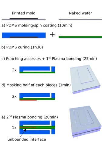
modifica-b) PDMS curing (1h30)
a) PDMS molding/spin coating (10min)
c) Punching accesses + 1st Plasma bonding (25min)
e) 2nd Plasma bonding (20min)
d) Masking half of each pieces (1min)
unbounded interface
f) Inlet/outlet tubes insersion and PDMS casting (1h50) Naked wafer Printed mold 2x 2x 1x 1x
+
Figure 1: Protocol for the realization of the nanopore chip microfluidic device (not to scale). a) (left) The printed mold is covered by PDMS. (right) A thin PDMS film is produced by spin coat-ing b) Curcoat-ing at 75oC. c) Plasma bonding (first) d) Masking e) Plasma bonding (second) f) Tube in-sertion and PDMS casting
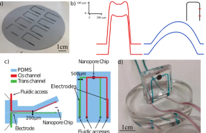
tions to the instructions code were made thanks to a custom program of our own. During the print, the substrate is heated up to 80oC to enhance print adhesion and limit the warping of printed objects due to the high temperature difference between the bottom of the object and the nozzle. Lastly, the freshly printed mold is heated up to 180oC for a few seconds using a hot plate. This last step is cru-cial in order to i) smooth the shape of the printed pattern and ii) achieve a good adherence of the PLA on the silicon wafer. Printed patterns were realized down to a width of 50 µm. However we chose to work with 150 µm wide channels as it in-duces less hydrodynamic resistance and make for more robust masters. The three inches master con-tains eight of those channels, for the mounting of a total of four devices (Figure 2a).
PDMS is used because of its insulating proper-ties as well as its fluidic sealing properproper-ties. We use Sylgard 184 (Dow Corning, U.S.A.) with a 10:1 base to curing agent ratio. After a thorough mixing, the solution is degassed at 300 mbar for 10-15min. The fabrication steps of the microflu-idic device we propose is detailed in Figure 1. The device is made of two identical PDMS sub-units corresponding to the cis and trans sides of the nanopore chip. The latter will be inserted in between these sub-units (Figure 1a and c). Each sub-unit is composed of two parts: one main part containing the channel and the other one a thin film for closing the channel. The first one is cast on a 3D-printed master (Figure 1a), the channels di-mensions are reported on Figure 2c. This layer should be around 5 mm high to be flexible enough to easily mount the nanopore chips without break-ing and still be durable. Fluidic access to the chan-nels are made at this step using a biopsy puncher. The thin film is spin-coated down to 200 µm over a naked silicon wafer (Figure 1a). PDMS is cured at 75oC for 1h30 (Figure 2b). Using a Basic Plasma Cleaner (Harrick Plasma, U.S.A.), the PDMS film is covalently bonded to the main part containing the channel to finalize the fabrication of each sub-unit (Figure 1c).
These sub-units are then partially bonded to-gether. First, the top half of both these parts is masked with tape (red line represented in Fig-ure 1d). Then, a second plasma activation bonds the unmasked bottom parts of the two sub-units.
1cm
1cm
Figure 2: PDMS based device for easy solid-state nanopore chip use. a) Picture of mold 3D-printed on a 3 in silicon wafer. Four devices can be as-sembled from the eight printed patterns. b) Pro-files of a 3D-printed mold before (red) and after melting. Two profiles are presented to show the uniformity of the printed parts, their location are approximately represented by red marks on the in-set. c) Side and top schematic view of the device. d) Picture of the device with a mounted nanopore chip.
The upper part (dotted red line in Figure 1e) re-mains open for nanopore chip insertion. Fluidic access tubes are inserted in the holes we previ-ously pierced. A talon of PDMS is cast to perfect their sealing (colored in orange in Figure 1f). For this, the device is put in a 2 in Petri dish which is then filled with PDMS. This talon also permits the device to stand for easy manipulations. Fi-nally, using a biopsy puncher again, apertures are made through the thin layer covering the channel in place of where the nanopore chip will be in-serted (Figure 2d). It will permit the analytes to reach the nanopore. To avoid any leaking during the changes of analytes, light pressure is applied to the upper part of the device thanks to two glass slates and a paper clip after nanopore mounting. This step is crucial to reversibly seal/detach the nanopore chips into/from the microfluidic device.
We use 3 mm silicon nitride chips (Nanopore solutions, Portugal) : these chips are composed of a 200 µm thick silicon substrate, covered by a 20 nm-thin Si3N4 layer. The substrate is etched in
its center to obtain a 15 × 15 µm2 free-standing
Si3N4membrane (Figure 3a).
Nanopores are all pierced thanks to a Titan Themis TEM mode at 8 nA. The size of the probe
is adapted to the desired pore size to obtain straight walls and a more stable pore. Thanks to the high currents used and the great control over the size of TEM beams, pores from 3 to 200 nm can be obtained rapidly.30Immediately after piercing, the
electron beam is defocused and we obtain an im-age of the pore. In this publication we use a 31 nm Si3N4pore (Figure 3).
PEG-7kDa (PolyPure AS, Norway) was grafted over the surface of the nanopore chip thanks to a three steps protocol already described in a previ-ous paper42,55 and is briefly reported in the
Sup-porting Information.
We use Ag/AgCl electrodes directly inserted in-side the channels of the device to measure the ionic current going through the pore. Current ampli-fication was done thanks to an Axopatch 200B (Molecular devices, U.S.A.). Data was acquired with a PCIe-6251 board (National Instruments, U.S.A.) interfaced with a custom .Net based pro-gram.
Current versus voltage curves (IVs) were ob-tained applying 30 s long voltage steps of 25 mV between ±200 mV. The current was recorded at 103samples/s and filtered thanks to the Axopatch 200B with a Bessel four poles low pass filter at 5 kHz. The average current for each voltage step is obtained from the last 15 s of the steps to avoid the expected capacitive surges induced by the changes of voltage. Finally, the slope of the IV curve yields the conductance of the pore according to the Ohm’s law. Typical recordings as well as the re-sulting IV curves are shown in Figure 4a and b.
Figure 3: Morphology of a nanopore chip. a) Stylized side-view of a nanopore chip grafted with PEG-7kDa. b) TEM view of the pierced pore be-fore grafting.
A schematics of a typical microfluidic system for solid-state nanopore measurements is shown in Figure S1. These systems are composed of two large compartments containing the electrolytes
separated by the nanopore chip. The main draw-back of such a system is that the change of analytes is done without a managed fluidic flow. The op-erator needs to change the electrolyte many times to avoid cross-contamination. Also, these systems often contain unreachable volumes of electrolytes, namely dead volumes, which accentuate this dis-advantage. The use of a grazing channel facilitates the change of electrolytes and ensures less cross-contamination. These channels are a typical solu-tion employed in microfluidics.
Previous approaches of printing microfluidic chips48,56or molds47with FDM printers show that the spatial resolution is limited to 200±100 µm de-pending on the 3D-printer used, with a roughness of 11 µm.48To rise up to this challenge, we chose to print the mold over a silicon wafer to take ad-vantage of the wafer nanometric smoothness. Af-ter printing, we melt the mold using a hot plate to enhance adhesion between the printed PLA and the silicon wafer. The profile of the 3D-printed mold has been measured thanks to a Dektak pro-filometer (Bruker, Germany) and is reported in Figure 2b. The height and width of the chan-nel are constant along a straight part with 213 ± 0.1 µm height and 826 ± 1 µm width measured on both profiles. Also we measured the rough-ness of the printed parts of the mold. We show that the heating step allows to decrease the chan-nel roughness from Rraw
a = 0.21 ± 0.1 µm and
Rqraw = 0.25 ± 0.1 µm to Rmelteda = 8 ± 4 nm and Rmelted
q = 10 ± 4 nm (calculus explained in
Sup-porting Information, Eq. 1). This low roughness allows for more durable molds as PDMS won’t clutch to it when removed.
The reversible sealing of the device has been tested thanks to a simple manometer. The device withstands to up to 2 bar without leaking. Most of the time, old devices or intensively used ones only leak from the entry point of the access tubes. Thus, measurements are still possible with small leakage.
This microfluidic device permitted to record ev-ery set of data used for a graph within 7 hours each. The study we describe in the next section has been done along 4 weeks, dismounting the same nanopore chip at the end of the day to safely store it between experiments. This shows the reliability of the device for the handling of the fragile chip.
Whereas obtaining high channels is costly and difficult with traditional photolithography meth-ods, our method allows for the fabrication of chan-nels up to 1 mm-high without hassle. An advan-tage of using high channels is their reduced hydro-dynamic resistance. Thanks to this, the filling of the microfluidic system and the change of analytes in this device takes only 6 to 10 s for 1 mL injec-tions by hand using a syringe. Also, we studied the effect of hemicylindrical channels on the fluidic flow using COMSOL Multiphysics finite elements simulations (COMSOL Group, Sweden). The flow speed and shear stress calculated for hemicylin-drical, rectangular and cylindrical channels having the same cross-section area are reported in Fig-ure S2. These simulations show the hemicylin-drical channel yields a hydrodynamic resistance 3% lower than the rectangular one for a straight channel. Furthermore, the shear stress is more ho-mogeneous along the wall in the hemicylindrical channel. Such homogeneity, especially along the walls of the channel is advantageous in tissue engi-neering, which is quite understandable as it corre-sponds to the shape of vascular vessels. A cylindri-cal channel allows for an even more homogeneous shear stress and a lesser hydrodynamic resistance. An assembly of two hemicylindrical channels ob-tained thanks to a 3D-printed mold could achieve such a channel. However, in our case, hemicylin-drical channels are more suited to the integration of a nanopore chip.
Grafting long polymer chains on nanopores tends to reduce their apparent size.26 Theses
chains presumably occupy space inside the pore and partially block the ion flux. The confor-mations of those chains inside or near the pore should greatly depend on their affinity with the electrolyte.57 We studied a Si3N4 31 nm pore
grafted with a long polymer: PEG-7kDa. Those pores have been characterized intensely through the study of their conductance in KCl and LiCl buffers at various salt concentrations (Figure 4). First, we plot the current traces at fixed voltages between −200 mV and +200 mV (Figure 4a). In figure 4a, we observe long fluctuations of the cur-rent in 10 mM LiCl. This behavior is discussed in the Supporting Information.
From the average value of the current trace, we plot the rectification parameter
|I(+200mV)/I(-Figure 4: Characterization of a hairy Si3N4
nanopore. a) Typical sequence of current measure-ments used to obtain one current versus voltage (IV) plot a hairy nanopore. Each trace in this graph corresponds to a voltage ranging from −200 mV (blue) to 200 mV (red) in a 10 mM LiCl buffer. b) IV plots obtained with 1 µM to 2 M LiCl. c) Recti-fication |I(+200 mV )/I(−200 mV )| of the same nanopore according to the KCl and LiCl concen-trations. d) Conductance of the pore at different KCl and LiCl concentrations showing the transi-tion between surface conductransi-tion at low concen-tration and ionic conduction at higher concentra-tions. Solutions were buffered by 5 mM Hepes at pH 7.4. Experiments are performed with a 31 nm wide nanopore grafted with PEG-7kDa in a 10 mM LiCl buffer.
200mV)| according to the LiCl or KCl concen-tration (Figure 4b). When we increase the LiCl concentration from 1 µM to 10 mM, the rectifica-tion decreases from 1.49 to 1.17. For concentra-tions larger than 10 mM, this rectification remains steady (1.14 ± 0.05). In presence of KCl, the rec-tification remains steady (1.08 ± 0.06) whatever the concentration. Considering the Debye length is larger than 3 nm if the salt concentration is smaller than 10 mM,51the electroosmotic flow could drag the grafted chains along the nanopore. In pres-ence of KCl, the K+cations are linked to the PEG chains, which are too strongly attracted to the neg-atively charged inner side of the nanopore to be dragged by the electroosmotic flow. In this case, we do not notice any current fluctuation.
Secondly, the average value of each current trace of the Figure 4a is used to plot the current-voltage characteristic curve (I-V curve) of the nanopore (Figure 4b). We observe a linear behavior of the ionic current versus the applied voltage : the ionic conductance through this channel follows the Ohm’s law. The IV-curve slope defines the con-ductance G of the nanopore.
We repeat these steps changing the salt concen-tration (1 µM < C < 2 M) and nature (LiCl or KCl) to obtain Figure 4d. This figure shows that the pore conductance G increases with salt concentration according to two regimes. At high concentrations (C > 0.1 M), the conductance in-creases linearly with the salt concentration thus be-ing governed by the bulk ionic transport. At low concentration, the conductance reaches a plateau and is dominated by the movement of counter-ions on the inner surface of the nanopore.
Pore size determination according to its ionic conductance is a frequently discussed matter.34,58,59 This conductance can be de-scribed by following simplified models.51,60
At high ionic concentration, the conductance is governed by the bulk conductivity K : Gvol= (π R2)/L × K where R is the radius
of the pore, L its length. Nevertheless, we must take the access conductance Gacc = 4 R K
of the nanopore into account.61 Considering
Gionic = 1/(1/Gvol+ 1/Gacc), we write :
Gionic= K L π R2 + 1 4 R (1)
In this regime, the bulk conductivity reads : K = (µ++ µ−) e2c (2)
where µ+ and µ− are the cation (µK+ = 4.76 ×
1011m2s−1J−1
, µLi+ = 2.50 × 10¹¹m2s−1J−1)
and the anion (µCl = 4.94 × 10¹¹m2s−1J−1)
mo-bilities respectively, e is the elementary charge and c the ion concentration (in ions per m3).
Now, we consider that the thickness h of the grafting is the same on the membrane and in the nanopore.60 Then, the apparent radius and length of the nanopore becomes R0 = R0 − h and L0 =
L0+2 h respectively after membrane coating, with
R0 and L0 the radius and length of the pore
be-fore grafting. From this, we can deduce a relation between the nanopore dimensions after grafting : L0 = L0+ 2 (R0 − R0). Finally, the equations (1)
and (2) become : G0ionic = (µ++ µ−) e2c L0+2 (R0−R0) π R02 + 1 4 R0 (3)
The fit of the experimental data (Figure 4d) leads to a decrease of the apparent radius of the nanopore after grafting RLiCl0 = 9.4 ± 0.6 nm in LiCl buffer and R0KCl = 12 ± 0.2 nm in KCl buffer. Thus, we estimate the thickness of the decorated membrane L0LiCl= 32.7 ± 1.2 nm and L0KCl = 27.5 ± 0.4 nm in LiCl and KCl buffer respectively. These results show that the grafted chain thickness is hLiCl = 5.6 ± 0.6 nm or
hKCl = 3 ± 0.2 nm in presence of LiCl or KCl
respectively.
Now, we discuss the conformation of the poly-mer chains grafted on the Si3N4 surface
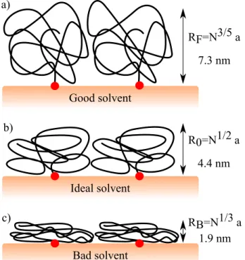
assum-ing that there is no overlappassum-ing between grafted chains.62–64 First, we could consider that these chains have better affinity with water molecules than with the membrane. In this case, they behave according to a good solvent conformation, as it is depicted in Figure 5. In this situation, the poly-mer chain has a better affinity for LiCl or KCl sol-vent than for itself. The chain size is character-ized by the Flory radius RF.65 With PEG-7kDa,
we calculate RF = 7.3 nm (Figure 5a). As RF
is larger than the grafted chain thickness, we can assume that the PEG-7kDa chains does not fol-low this regime. Then, we could consider
inter-RF=N3/5 a 7.3 nm Good solvent a) RB=N1/3 a 1.9 nm Bad solvent c) R0=N1/2 a 4.4 nm Ideal solvent b)
Figure 5: Conformations of polymer chain grafted on Si3N4 membrane a) behavior in good solvent
regime b) in ideal solvent regime c) in bad sol-vent regime. N is the number of monomeric units of length a. Calculations are perform with PEG-7kDa chain (N = 159, a = 0.35 nm).
actions between polymer chains and the solvent are balanced with the ones with the membrane. In this situation, the polymer chain could be con-sidered as an ideal one characterized by the ideal radius R0 (Figure 5b). As R0 = 4.4 nm, we
could consider that the polymer chains behaves as ideal polymer brush only in presence of LiCl (hLiCl > R0), whereas it is not the case in
pres-ence of KCl (hKCl < R0). In the latter case, the
PEG chains seem to be collapsed on the membrane in presence of KCl (Figure 5c). In this situation, the polymer chains are more attracted by the Si3N4
surface than by the aqueous phase, and behaves as in bald solvent regime. This behavior could be due to the binding of K+ cations.66,67 Then, the
chains adopt a cigar-like shape, as it was previ-ously described in.66 The PEG chains behave as positive polyelectrolytes in KCl, which increases their attractions with the negatively charged silanol groups on the membrane surface.68These observa-tions show that the conformation of grafted PEG chains is controlled by the electrolyte: apparent ideal chain in LiCl and apparent collapsed chain
in KCl.
At low ionic concentration, the conductance is dominated by surface effects due to the presence of counter-ions on the inner surface of the nanopore. It reads :
Gs =
2πR0 L0
µ+e σ (4)
with σ the surface charge of the pore, µ+
the ionic mobility of the positive counter-ions, considering that the negative charge sur-face is due to the the dissociation of silanol groups.68 At low salt concentrations, we
can see on Figure 4 that the pore yields a lower conductance with LiCl than with KCl : GLiCl
s = 5.4 ± 0.1 nS and GKCls = 9.4 ± 0.2 nS.
According to Eq. (4), we calculate the corre-sponding surface charge : σLiCl= 46 ± 6 mC/m2
and σKCl = 33 ± 3 mC/m2. The surface charge
of the grafted nanopore is not dependent on LiCl or KCl concentration. These values are in good agreement with the one measured with shorter PEG chain,26but they are smaller than the surface
charge measured with uncoated Si3N4 channels
σSiN = 60 mC/m2.50 This decrease could be
ex-plained by the polymer chain brush covering the inner side of the nanopore. Moreover, this screen-ing effect could be enhanced by the formation of K+/PEG complexes in presence of KCl (decrease from 60 to 33 mC/m2).66
Now, we propose to use this nanopore to charac-terize interactions between proteins and urea at the nanometer scale. Protein denaturation is usually performed with urea addition. Nevertheless this process is not yet well understood. Two mecha-nisms are usually described:69the first one is based on the disruption of the structure of water around the protein, which increases the solubility of hy-drophobic groups.70 These bindings would lead to the entering of urea into the unfolded protein. Thus, urea would behave as a surfactant between the protein and water.71 The second mechanism is based on direct interactions between urea and the protein.72
In this work, PEG chains act as a model chain to mimic interactions of proteins with urea or wa-ter. As the electrical detection coupled with mi-crofluidic integration allows to precise the PEG conformation, we use this method to determine the PEG chain conformation in presence of LiCl
a) 10 5 0 -5 -10 Current (nA) -200 -100 0 100 200 Voltage (mV) 0M 10mM 100mM 500mM 1M 2M 3M 4M 5M 6M 7M 8M 9M b) c) e) d) 10mM LiCl 0.5M KCl 0.5M LiCl 10mM KCl 220 200 180 160 140 120 100 Pore Conductance (nS) 9 8 7 6 5 4 3 2 1 0 Urea Concentration (M) Measured Calculated 50 45 40 35 30 25 Pore Conductance (nS) 9 8 7 6 5 4 3 2 1 0 Urea Concentration (M) Measured Calculated 22 20 18 16 14 12 10 Pore Conductance (nS) 9 8 7 6 5 4 3 2 1 0 Urea Concentration (M) Measured Calculated 13 12 11 10 9 8 7 6 Pore Conductance (nS) 9 8 7 6 5 4 3 2 1 0 Urea Concentration (M) Measured Calculated
Figure 6: Interactions of urea with polymer brushes in confined medium. a) IV curves ob-tained with urea concentrations ranging from 10 mM to 9 M at 0.5 M LiCl. Pore conductance (plotted with circle markers) versus urea concen-tration at b) 0.5 M LiCl, c) 0.5 M KCl d) 10 mM LiCl e) 10 mM KCl. The conductance calculated from bulk conductivity (Eq. 5) is plotted with square markers. All experiments were performed in buffered solution with 5 mM Hepes at pH 7.5.
or KCl. Firstly, we consider the high salt concen-tration where the conductance is governed by the ionic flow. We plot IV-curves in a 0.5 M LiCl so-lution by increasing the urea concentration from 0 M to 9 M (Figure 6a and S5). As we do not notice current rectification, we use the slope of each IV-curve to calculate the nanopore conduc-tance. In presence of 0.5M LiCl, we observe that the nanopore conductance decreases linearly from 52.1 ± 0.1 nS to 25 ± 2.3 nS when urea concen-tration goes from 0 up to 9 M (Figure 7b). As the ionic mobility is inversely proportional to the vis-cosity, this decrease could be due to the viscosity increase, when we increase the urea concentration. To answer this assumption, we consider a conduc-tance Gv calculated from conductivity K of the
urea solution :
Gv =
K Kb
Gb (5)
with Gb and Kb the pore conductance and the
electrolyte conductivity without urea respectively. This relation, based only on the viscosity varia-tions, is plotted in Figure 6b with square mark-ers. At 0.5 M LiCl, there is a good agreement between conductance measurements, plotted with circle markers, and calculated conductance Gv.
We observe the same behavior at 0.5 M KCl (Fig-ure 6c). Then, we repeat these meas(Fig-urements at low salt concentration where the conductance is dominated by counter-ions, i.e. charge density on the inner side of the nanopore. We observe the same behavior with 10 mM KCl (Figure 6e), but the conductance does not decrease as much as ex-pected as the viscosity increases when we add urea in presence of 10 mM LiCl (Figure 6d).
Then, we normalize the conductance G with the conductance Gv calculated above (Eq. 5) to know
if the conductance variations are due to viscosity or to geometrical ones :
GN =
G Gv
(6)
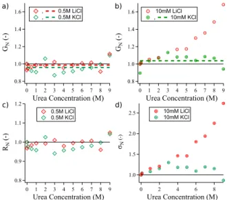
Considering the regime of high ionic concentra-tions, we observe that the normalized conductance GN is constant GN = 0.99 ± 0.05 at 0.5 M LiCl
(Figure 7a). In this regime, the conductance in-side the nanopore is mainly governed by the ionic
flow. We could neglect the effects due to the sur-face conductance of the pore. According to Eq. 3, GN is just function of the geometrical dimensions
of the nanopore. Then, we define the normalized radius :
RN =
R0 Rb
(7)
where R0 and Rb represent the apparent nanopore
radius with or without urea respectively, calcu-lated from Eq. 3. In Figure 7c, this normalized radius is steady when the urea concentration in-creases RN = 0.99 ± 0.02. Then, we could
sup-pose that urea has no action on the pore sizes and doesn’t affect the conformation of PEG chains at high LiCl concentrations. We observe the same behavior in presence of 0.5 M KCl (Figure 7a). In this case, the normalized conductance does not vary (GN = 0.96 ± 0.07). Then, we plot the
nor-malized radius according to Eq. 7 versus the urea concentration. It is constant RN = 0.98 ± 0.03.
Then, urea seems to not affect the conformation of grafted PEG chains in presence of KCl, as it was the case with LiCl.
Now, we could consider the regime of low ionic concentrations. If we plot the normalized conduc-tance GN, we observe that it increases with urea
concentration (Figure 7b). Considering that the nanopore radius is not modified by the increase of urea concentration, this increase could be due to the increase of counter-ion charge according to Eq. 4. Then, we define a normalized surface charge:
σN =
σ σb
(8)
where σ and σb represent the nanopore charge
sur-face with or without urea respectively, calculated from Eq. 4. σN increases with urea concentration
until 2.7 times at 9 M urea (Figure 7d). This strong increase could be explained by the high dipole mo-ment of urea (4.56 D), which is 2.5 times higher than the water one (1.85 D). Then, we could sup-pose that urea could replace water inside the PEG brush and modify strongly the counter-ions distri-bution inside the nanopore.
Now, we consider the experiments performed with 10 mM KCl. We observe that the normal-ized conductance of the pore doesn’t increase with urea concentration : GN = 1.03±0.07 (Figure 7b).
gov-a) b) d) c) 1.6 1.4 1.2 1.0 0.8 GN (-) 9 8 7 6 5 4 3 2 1 0 Urea Concentration (M) , 0.5M LiCl , 0.5M KCl 1.6 1.4 1.2 1.0 0.8 GN (-) 9 8 7 6 5 4 3 2 1 0 Urea Concentration (M) 10mM LiCl , 10mM KCl 1.2 1.1 1.0 0.9 0.8 RN (-) 9 8 7 6 5 4 3 2 1 0 Urea Concentration (M) 0.5M LiCl 0.5M KCl 2.5 2.0 1.5 1.0 σN (-) 8 6 4 2 0 Urea Concentration (M) 10mM LiCl 10mM KCl
Figure 7: Normalized pore conductance as a func-tion of urea concentrafunc-tion at a) 0.5 M LiCl and KCl and b) 10 mM LiCl and KCl. The dotted lines represents the average values of the conductance. None have been plotted for 10 mM LiCl. The plain black line represents the expected value of GN = 1. c) Normalized pore radius at 0.5 M LiCl
and KCl at various urea concentrations. d) Nor-malized surface charge of the nanopore at 10 mM LiCl and KCl at various urea concentrations.
erned by the counter-ions, we plot the normalized charge surface σN in Figure 7d. As σN is steady
σN = 1.08 ± 0.15, the surface charge seems to
not be modified by the addition of urea. Con-trary to the observations performed with LiCl, urea molecules seem to not replace the water ones in-side the PEG brush in presence of KCl. These ob-servations could be explained by considering the PEG conformation. Previously, we have shown that the PEG chains are strongly attracted to the Si3N4 surface in presence of KCl. Then, in that
state the polymer brush behaves like in an apparent bad solvent. In this collapsed conformation, we could suppose urea can’t go inside the PEG brush to replace water.
We designed and manufactured a cheap mi-crofluidic master from an easy and fast 3D-printer-based protocol for the reversible integration of a solid-state nanopore chip. This device per-mits to quickly perform a large series of electri-cal measurements in different environments (na-ture and concentration of salt, urea) without disas-sembling the nanopore from the microfluidic
sys-tem. Also, our device could be used to rapidly pierce nanopores thanks to the dielectric break-down method35–37 to be then stored for future
use. We found that, at low salt concentrations, the conductance is dominated by the movement of counter-ions on the inner surface of the nanopore and that at high concentrations, the conductance is governed by the bulk ionic transport. From elec-trical measurements we can deduce the conforma-tion of the polymer chains grafted on the nanopore surface. At high ionic concentration, the polymer chains behave as ideal polymer brush or as a cigar-like shape respectively in presence of LiCl or KCl. For ideal chains, urea molecules can stand in for the water molecules leading to an increase of the apparent charge of the polymer-grafted surface. On the other hand, if the chain is collapsed, the urea molecule cannot enter into the chain and thus don’t change its conformation nor its polarisabil-ity. This biomimetic system allows to enhance our understanding of interactions between urea and proteins. In our case, the PEG chains in presence of LiCl are similar to the hydrophilic domains of the protein whereas in presence of KCl they be-have like the hydrophobic domains. This experi-mental study is in good agreement with previous simulations of protein denaturation with urea.69,72
Nevertheless, we did not observe the penetration of urea into the hydrophobic core.72
The authors declare no competing financial in-terest.
Acknowledgement This research was supported by the "DEFI CNRS Instrumentation aux limites" 2016 & 2017 and by ANR Epsilomics (ANR-17-CE09-0044-02). We thank Johanna Canovas, Rasta Ghasemi and Abdelghani Oukhaled for their assistance. This publication is dedicated to Loïc Auvray’s memory.
Supporting Information
Avail-able
The Supporting Information is available free of charge on the ACS Publications website at DOI:
Description of a traditional flow-cell; Calcula-tion of the roughness measurement; Flow sim-ulation in microfluidic channels; Current traces
and fluctuations with hairy nanopore; Conduc-tance measurement in urea;
References
(1) Lepoitevin, M.; Ma, T.; Bechelany, M.; Janot, J.-M.; Balme, S. Functionalization of single solid state nanopores to mimic biological ion channels: A review. Adv. Colloid Interface Sci. 2017, 250, 195–213.
(2) Shi, W.; Friedman, A. K.; Baker, L. A. Nanopore Sensing. Analytical Chemistry 2017, 89, 157– 188.
(3) Wang, Y.; Zheng, D.; Tan, Q.; Wang, M. X.; Gu, L.-Q. Nanopore-based detection of circulat-ing microRNAs in lung cancer patients. Nat Nano 2011, 6, 668–674.
(4) Lin, Y.; Ying, L.; Shi, X.; Liu, S.-C.; Long, Y.-T. Direct sensing of cancer biomarkers in clin-ical samples with a designed nanopore. Chem Commun 2017, 53, 11564–11567.
(5) Coulter, W. H. Means for counting particles sus-pended in a fluid. 1953.
(6) Larkin, J.; Henley, R. Y.; Muthukumar, M.; Rosenstein, J. K.; Wanunu, M. High-Bandwidth Protein Analysis Using Solid-State Nanopores. Biophysical Journal 2014, 106, 696–704.
(7) Plesa, C.; Cornelissen, L.; Tuijtel, M. W.; Dekker, C. Non-equilibrium folding of individual DNA molecules recaptured up to 1000 times in a solid state nanopore. Nanotechnology 2013, 24, 475101–475108.
(8) Varongchayakul, N.; Huttner, D.; Grin-staff, M. W.; Meller, A. Sensing Native Protein Solution Structures Using a Solid-state Nanopore: Unraveling the States of VEGF. Sci. Rep. 2018, 8, 1017–1025.
(9) Steinbock, L. J.; Otto, O.; Skarstam, D. R.; Jahn, S.; Chimerel, C.; Gornall, J. L.; Keyser, U. F. Probing DNA with micro- and nanocapillaries and optical tweezers. J Phys : Condens Matter 2010, 22, 454113–454120. (10) Saleh, O. A.; Sohn, L. L. Direct detection of
antibody-antigen binding using an on-chip artifi-cial pore. Proc. Natl. Acad. Sci. U. S. A. 2003, 100, 820–824.
(11) Halpern, A. R.; Donavan, K. C.; Penner, R. M.; Corn, R. M. Wafer-scale fabrication of nanoflu-idic arrays and networks using nanoimprint lithography and lithographically patterned nanowire electrodeposition gold nanowire masters. Anal. Chem. 2012, 84, 5053–5058. (12) Angeli, E.; Volpe, A.; Fanzio, P.; Repetto, L.;
Firpo, G.; Guida, P.; Lo Savio, R.; Wanunu, M.; Valbusa, U. Simultaneous Electro-Optical Track-ing for Nanoparticle Recognition and CountTrack-ing. Nano Letters 2015, 15, 5696–5701.
(13) Siwy, Z.; Fulinski, A. Fabrication of a synthetic nanopore ion pump. Phys. Rev. Lett. 2002, 89, 198103–198106.
(14) Yameen, B.; Ali, M.; Neumann, R.; Ensinger, W.; Knoll, W.; Azzaroni, O. Single conical nanopores displaying pH-tunable rectifying characteristics. manipulating ionic transport with zwitterionic polymer brushes. J. Am. Chem. Soc. 2009, 131, 2070–2071.
(15) Guo, W.; Tian, Y.; Jiang, L. Asymmetric Ion Transport through Ion-Channel-Mimetic Solid-State Nanopores. Acc. Chem. Res. 2013, 46, 2834–2846.
(16) Balme, S.; Picaud, F.; Manghi, M.; Palmeri, J.; Bechelany, M.; Cabello-Aguilar, S.; Abou-Chaaya, A.; Miele, P.; Balanzat, E.; Janot, J. M. Ionic transport through sub-10 nm diameter hy-drophobic high-aspect ratio nanopores: experi-ment, theory and simulation. Sci. Rep. 2015, 5, 10135–10148.
(17) Bacri, L.; Benkhaled, A.; Guegan, P.; Auvray, L. Ionic channel behavior of modified cyclodextrins inserted in lipid membranes. Langmuir 2005, 21, 5842–5846.
(18) Geng, J.; Kim, K.; Zhang, J.; Escalada, A.; Tunuguntla, R.; Comolli, L. R.; Allen, F. I.; Shny-rova, A. V.; Cho, K. R.; Munoz, D.; Wang, Y. M.; Grigoropoulos, C. P.; Ajo-Franklin, C. M.; Frolov, V. A.; Noy, A. Stochastic transport through carbon nanotubes in lipid bilayers and live cell membranes. Nature 2014, 514, 612–615. (19) Mamad-Hemouch, H.; Ramoul, H.; Abou Taha, M.; Bacri, L.; Huin, C.; Przybylski, C.; Oukhaled, A.; Thiébot, B.; Patriarche, G.; Jar-roux, N.; Pelta, J. Biomimetic Nanotubes Based
on Cyclodextrins for Ion-Channel Applications. Nano Letters 2015, 15, 7748–7754.
(20) Goepfrich, K.; Li, C.-Y.; Ricci, M.; Bhamidi-marri, S. P.; Yoo, J.; Gyenes, B.; Ohmann, A.; Winterhalter, M.; Aksimentiev, A.; Keyser, U. F. Large-Conductance Transmembrane Porin Made from DNA Origami. ACS Nano 2016, 10, 8207– 8214.
(21) Bezrukov, S. M.; Vodyanoy, I.; Parsegian, V. A. Counting polymers moving through a single ion channel. Nature 1994, 370, 279–281.
(22) Wang, H.; Ettedgui, J.; Forstater, J.; Robert-son, J. W. F.; Reiner, J. E.; Zhang, H.; Chen, S.; Kasianowicz, J. J. Determining the Physical Prop-erties of Molecules with Nanometer-Scale Pores. ACS Sensors 2018, 3, 251–263.
(23) Li, J.; Stein, D.; McMullan, C.; Branton, D.; Aziz, M. J.; Golovchenko, J. a. Ion-beam sculpt-ing at nanometre length scales. Nature 2001, 412, 166–169.
(24) Bacri, L.; Oukhaled, A. G.; Schiedt, B.; Patri-arche, G.; Bourhis, E.; Gierak, J.; Pelta, J.; Au-vray, L. Dynamics of colloids in single solid-state nanopores. J. Phys. Chem. B 2011, 115, 2890– 2898.
(25) Cressiot, B.; Oukhaled, A.; Patriarche, G.; Pastoriza-Gallego, M.; Betton, J.-M.; Auvray, L.; Muthukumar, M.; Bacri, L.; Pelta, J. Protein Transport through a Narrow Solid-State Nanopore at High Voltage: Experiments and Theory. ACS Nano 2012, 6, 6236–6243.
(26) Giamblanco, N.; Coglitore, D.; Janot, J. M.; Coulon, P. E.; Charlot, B.; Balme, S. Detection of protein aggregate morphology through single antifouling nanopore. Sensors and Actuators, B: Chemical 2018, 260, 736–745.
(27) Oukhaled, A.; Cressiot, B.; Bacri, L.; Pastoriza-Gallego, M.; Betton, J.-M.; Bourhis, E.; Jede, R.; Gierak, J.; Auvray, L.; Pelta, J. Dynamics of Completely Unfolded and Native Proteins through Solid-State Nanopores as a Function of Electric Driving Force. ACS Nano 2011, 5, 3628– 3638.
(28) Waduge, P.; Hu, R.; Bandarkar, P.; Yamazaki, H.; Cressiot, B.; Zhao, Q.; Whitford, P. C.; Wa-nunu, M. Nanopore-Based Measurements of
Protein Size, Fluctuations, and Conformational Changes. ACS Nano 2017, 11, 5706–5716. (29) Larkin, J.; Henley, R.; Bell, D. C.;
Cohen-Karni, T.; Rosenstein, J. K.; Wanunu, M. Slow DNA Transport through Nanopores in Hafnium Oxide Membranes. ACS Nano 2013, 7, 10121– 10128.
(30) Storm, A. J.; Chen, J. H.; Ling, X. S.; Zandber-gen, H. W.; Dekker, C. Fabrication of solid-state nanopores with single-nanometre precision. Nat. Mater. 2003, 2, 537–540.
(31) Baaken, G.; Halimeh, I.; Bacri, L.; Pelta, J.; Oukhaled, A.; Behrends, J. C. High-Resolution Size-Discrimination of Single Nonionic Syn-thetic Polymers with a Highly Charged Biological Nanopore. ACS Nano 2015, 9, 6443–6449. (32) Peraro, M. D.; van der Goot, F. G. Pore-forming
toxins: ancient, but never really out of fashion. Nat. Rev. Microbiol. 2016, 14, 77–92.
(33) Wanunu, M.; Dadosh, T.; Ray, V.; Jin, J.; Mcreynolds, L.; Drndic, M. microRNAs using thin nanopore sensors. Nature Nanotechnology 2010, 5, 807–814.
(34) Lee, C.; Joly, L.; Siria, A.; Biance, A.-L.; Ful-crand, R.; Bocquet, L. Large apparent electric size of solid-state nanopores due to spatially extended surface conduction. Nano Lett. 2012, 12, 4037– 4044.
(35) Kwok, H.; Briggs, K.; Tabard-Cossa, V. Nanopore fabrication by controlled dielectric breakdown. PLoS One 2014, 9, e92880–e92885. (36) Feng, J.; Liu, K.; Graf, M.; Dumcenco, D.;
Kis, A.; Di Ventra, M.; Radenovic, A. Obser-vation of ionic Coulomb blockade in nanopores. Nat. Mater. 2016, 15, 850–855.
(37) Lin, Y.; Shi, X.; Liu, S.-C.; Ying, Y.-L.; Li, Q.; Gao, R.; Fathi, F.; Long, Y.-T.; Tian, H. Char-acterization of DNA duplex unzipping through a sub-2 nm solid-state nanopore. Chem. Commun. 2017, 53, 3539–3542.
(38) Niedzwiecki, D. J.; Grazul, J.; Movileanu, L. Single-molecule observation of protein adsorp-tion onto an inorganic surface. Journal of the American Chemical Society 2010, 132, 10816– 10822.
(39) Wanunu, M.; Meller, A. Chemically modified solid-state nanopores. Nano Lett. 2007, 7, 1580– 1585.
(40) Kowalczyk, S. W.; Kapinos, L.; Blosser, T. R.; Magalhaes, T.; van Nies, P.; Lim, R. Y. H.; Dekker, C. Single-molecule transport across an individual biomimetic nuclear pore complex. Nat. Nanotechnol. 2011, 6, 433–438.
(41) Ketterer, P.; Ananth, A. N.; Laman Trip, D. S.; Mishra, A.; Bertosin, E.; Ganji, M.; van der Torre, J.; Onck, P.; Dietz, H.; Dekker, C. DNA origami scaffold for studying intrinsically disor-dered proteins of the nuclear pore complex. Nat Commun 2018, 9, 902–908.
(42) Roman, J.; Jarroux, N.; Patriarche, G.; Français, O.; Pelta, J.; Le Pioufle, B.; Bacri, L. Functionalized Solid-State Nanopore Inte-grated in a Reusable Microfluidic Device for a Better Stability and Nanoparticle Detection. ACS Applied Materials & Interfaces 2017, 41634–41640.
(43) Yin, B.; Xie, W.; Liang, L.; Deng, Y.; He, S.; He, F.; Zhou, D.; Tlili, C.; Wang, D. Cova-lent Modification of Silicon Nitride Nanopore by Amphoteric Polylysine for Short DNA Detection. ACS Omega 2017, 2, 7127–7135.
(44) Tahvildari, R.; Beamish, E.; Tabard-Cossa, V.; Godin, M. Integrating nanopore sensors within microfluidic channel arrays using controlled breakdown. Lab on a Chip 2015, 15, 1407–1411. (45) Tahvildari, R.; Beamish, E.; Briggs, K.;
Chagnon-Lessard, S.; Sohi, A. N.; Han, S.; Watts, B.; Tabard-Cossa, V.; Godin, M. Manipulating Elec-trical and Fluidic Access in Integrated Nanopore-Microfluidic Arrays Using Microvalves. Small 2016, 13, 1602601–1602607.
(46) Duffy, D. C.; McDonald, J. C.; Schueller, O. J. A.; Whitesides, G. M. Rapid prototyping of microfluidic systems in poly(dimethylsiloxane). Analytical Chemistry 1998, 70, 4974–4984. (47) Mcdonald, J. C.; Chabinyc, M. L.;
Met-allo, S. J.; Anderson, J. R.; Stroock, A. D.; White-sides, G. M. Prototyping of Microfluidic Devices in Poly ( dimethylsiloxane ) Using Solid-Object Printing the fabrication of microfluidic devices in poly ( dimethyl-. Analytical chemistry 2002, 74, 1537–1545.
(48) Macdonald, N. P.; Cabot, J. M.; Smejkal, P.; Guijt, R. M.; Paull, B.; Breadmore, M. C. Comparing Microfluidic Performance of Three-Dimensional (3D) Printing Platforms. Analytical Chemistry 2017, 89, 3858–3866.
(49) Peleg, O.; Tagliazucchi, M.; Kroeger, M.; Ra-bin, Y.; Szleifer, I. Morphology Control of Hairy Nanopores. ACS Nano 2011, 5, 4737–4747. (50) Stein, D.; Kruithof, M.; Dekker, C.
Surface-charge-governed ion transport in nanofluidic channels. Phys. Rev. Lett. 2004, 93, 035901– 035904.
(51) Schoch, R. B.; Han, J.; Renaud, P. Transport phenomena in nanofluidics. Reviews of Modern Physics 2008, 80, 839–883.
(52) Myers, J. K.; Pace, C. N.; Scholtz, J. M. Denatu-rant m values and heat capacity changes: Relation to changes in accessible surface areas of protein unfolding. Protein Science 1995, 4, 2138–2148. (53) Vanzi, F.; Madan, B.; Sharp, K. Effect of the
Pro-tein Denaturants Urea and Guanidinium on Wa-ter Structure: A Structural and Thermodynamic Study. Journal of the American Chemical Society 1998, 120, 10748–10753.
(54) Bennion, B. J.; Daggett, V. The molecular basis for the chemical denaturation of proteins by urea. Proceedings of the National Academy of Sciences 2003, 100, 5142–5147.
(55) Yang, H.; Zhang, G.; Hong, X.; Zhu, Y. Sily-lation of mesoporous silica MCM-41 with the mixture of Cl(CH2)3SiCl3 and CH3SiCl3: com-bination of adjustable grafting density and im-proved hydrothermal stability. Microporous and Mesoporous Materials 68, 119–125.
(56) Tang, C. K.; Vaze, A.; Rusling, J. F. Automated 3D-printed unibody immunoarray for chemilumi-nescence detection of cancer biomarker proteins. Lab Chip 2017, 17, 484–489.
(57) Milner, S. T. Polymer Brushes. Science 1991, 251, 905–914.
(58) Ma, Y.; Guo, J.; Jia, L.; Xie, Y. Entrance Effects Induced Rectified Ionic Transport in a Nanopore/Channel. ACS Sensors 2018, 3, 167– 173.
(59) Wen, C.; Zhang, Z.; Zhang, S. L. Physical Model for Rapid and Accurate Determination of Nanopore Size via Conductance Measurement. ACS Sensors 2017, 2, 1523–1530.
(60) Frament, C. M.; Bandara, N.; Dwyer, J. R. Nanopore Surface Coating Delivers Nanopore Size and Shape through Conductance-Based Siz-ing. ACS Applied Materials & InterfacesApplied Materials & Interfaces 2013, 5, 9330–9337. (61) Hall, J. E. Access resistance of a small circular
pore. The Journal of General Physiology 1975, 66, 531–532.
(62) Alexander, S. Adsorption of chain molecules with a polar head a scaling description. 1977, 38, 983– 987.
(63) Gennes, P. G. D. Conformations of Polymers At-tached to an Interface. Macromolecules 1980, 13, 1069–1075.
(64) Auroy, P.; Auvray, L.; Léger, L. Characterization of the brush regime for grafted polymer layers at the solid-liquid interface. Physical Review Letters 1991, 66, 719–722.
(65) De Gennes, P. G. Scaling Concepts in Polymer Physics; Cornell University Press, Ithaca, NY, 1979.
(66) Reiner, J. E.; Kasianowicz, J. J.; Nablo, B. J.; Robertson, J. W. F. Theory for polymer analysis using nanopore-based single-molecule mass spec-trometry. Proc. Natl. Acad. Sci. U. S. A. 2010, 107, 12080–12085.
(67) Breton, M. F.; Discala, F.; Bacri, L.; Foster, D.; Pelta, J.; Oukhaled, A. Exploration of Neutral Versus Polyelectrolyte Behavior of Poly(ethylene glycol)s in Alkali Ion Solutions using Single-Nanopore Recording. The Journal of Physical Chemistry Letters 2013, 4, 2202–2208.
(68) Behrens, S. H.; Grier, D. G. The charge of glass and silica surfaces. Journal of Chemical Physics 2001, 115, 6716–6721.
(69) Xia, Z.; Das, P.; Shakhnovich, E. I.; Zhou, R. Col-lapse of unfolded proteins in a mixture of denatu-rants. Journal of the American Chemical Society 2012, 134, 18266–18274.
(70) Hammes, G. G.; Schimmel, P. R. An Investiga-tion of Water-Urea and Water-Urea-Polyethylene Glycol Interactions. J. Am. Chem. Soc. 1967, 89, 442–446.
(71) Zangi, R.; Zhou, R.; Berne, B. J. Urea’s ac-tion on hydrophobic interacac-tions. Journal of the American Chemical Society 2009, 131, 1535– 1541.
(72) Hua, L.; Zhou, R.; Thirumalai, D.; Berne, B. J. Urea denaturation by stronger dispersion interac-tions with proteins than water implies a 2-stage unfolding. Proceedings of the National Academy of Sciences 2008, 105, 16928–16933.