HAL Id: hal-01222998
https://hal.archives-ouvertes.fr/hal-01222998
Submitted on 3 Feb 2016
HAL is a multi-disciplinary open access
archive for the deposit and dissemination of
sci-entific research documents, whether they are
pub-lished or not. The documents may come from
teaching and research institutions in France or
abroad, or from public or private research centers.
L’archive ouverte pluridisciplinaire HAL, est
destinée au dépôt et à la diffusion de documents
scientifiques de niveau recherche, publiés ou non,
émanant des établissements d’enseignement et de
recherche français ou étrangers, des laboratoires
publics ou privés.
Self-ordered arrays of linear defects and virtual
singularities in thin smectic-A films
Bruno Zappone, Emmanuelle Lacaze, Habib Hayeb, Michel Goldmann,
Nathalie Boudet, Philippe Barois, Michel Alba
To cite this version:
Bruno Zappone, Emmanuelle Lacaze, Habib Hayeb, Michel Goldmann, Nathalie Boudet, et al..
Self-ordered arrays of linear defects and virtual singularities in thin smectic-A films. Soft Matter, Royal
Society of Chemistry, 2011, 7 (3), pp.1161-1167. �10.1039/c0sm00747a�. �hal-01222998�
CREATED USING THE RSC ARTICLE TEMPLATE (VER. 3.1) - SEE WWW.RSC.ORG/ELECTRONICFILES FOR DETAILS
ARTICLE TYPE www.rsc.org/xxxxxx | XXXXXXXX
Self-ordered arrays of linear defects and virtual singularities
in thin smectic-A films
Bruno Zappone,*
aEmmanuelle Lacaze,*
bHabib Hayeb,
bMichel Goldmann,
b,cNathalie Boudet,
dPhilippe
Barois
dand Michel Alba
eReceived (in XXX, XXX) Xth XXXXXXXXX 200X, Accepted Xth XXXXXXXXX 200X 5
First published on the web Xth XXXXXXXXX 200X DOI: 10.1039/b000000x
Large-area ordered arrays can be created by the self-assembly of linear defects in thin Smectic-A films deposited in air on crystalline substrates. Such structu res could find applications in nanoparticle assembly and soft lithography. The smectic layers are bent in concentric cylinders
10
under the effect of conflicting strong anchoring conditions at the substrate surface and free interface, and neighboring cylindrical domains are separated by curvature walls. We have studied the internal structure of such domains near the surface of muscovite mica using synchrotron x -ray diffraction. Our findings show that the domains are centered on virtual singularities, running b elow the substrate plane, and rest upon a surface region of submicrometric thickness where layers are
15
flat and vertical, satisfying the planar anchoring condition imposed by the substrate.
Introduction
Creating large-scale ordered structures from the self-assembly of small building blocks such as copolymers1 and liquid
20
crystals2 is an exciting possibility for material science and nanotechnology. The "bottom-up" organization of organic materials is faster, less expensive and can produce more complex geometries than traditional "top-down'" microfabrication methods such as lithography. Liquid crystal
25
structures offer the additional benefit of responsiveness to external stimuli such as electromagnetic, mechanical and thermal fields, which can produce structural changes at various length scales (phase transitions, orientational transitions, pattern growth)3. In the past few years,
30
thermotropic smectic-A liquid crystal (SmA) have been used to create self-ordered templates for soft lithography4 or direct the dispersion and assembly of colloids5 and nanoparticles6. Rod-like SmA molecules form layers of nanometric thickness comparable to the molecule length, and align parallel to each
35
other along a preferential direction ("director") normal to the layers, determined by the boundary conditions ("anchoring").3
__________________________________________________
40
a LICRYL, IPCF-CNR, c/o Università della Calabria, cubo 33/B, Rende (CS) 87036 Italy. Fax: +39 0984 494401; Tel: +39 0984 496150; E-mail: [email protected]
b INSP, CNRS UMR-7588, Université Pierre et Marie Curie – Paris 6,
45
Paris, France Fax: +33 1 43542878; Tel: +33 1 44274654; E-mail: [email protected].
c Université Paris Descartes, 45 rue des Saint Pères, 75006 Paris Cedex, France
d Université Bordeaux 1, Centre de Recherche Paul Pascal, CNRS
UPR-50
8641, Pessac, France
e Laboratoire Léon Brillouin, CEA-CNRS, Saclay, France
d Institut NEEL/CNRS-UJF, 25 rue des Martyrs, 38042 Grenoble, France 55
Under the effect of incompatible but equally strong anchoring conditions, the layered structure becomes distorted. Layers are easily bent in the bulk but compression and dilation – requiring a high energy per unit volume – are confined to singular lines and walls ("defects") of nanometric extent.7
60
Colloids and nanoparticle interact with defects5 and may become trapped at the intersection of defects and boundaries.8 It is therefore crucial to understand defect-surface interaction, especially in SmA liquid crystals where interfaces are expected to deeply affect the defect structure.8-10
65
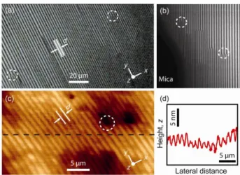
Fig. 1 Arrays of parallel linear domains of SmA 8CB on mica. The
domain axis, y, is perpendicular to the direction x of planar anchoring. d is the distance between neighboring disclinations. Circles mark regions where domains split or merge. (a) Optical micrograph of an array between
70
crossed polarizers. (b) Detail of a drop edge. (c) AFM topographic image of the free interface. (d) Modulation of height z as a function of the distance obtained from fig. (c) along the dashed line.
Fig. 2 (a) Model array of cylindrical domains with disclination centres
(blue dots) tangent to the substrate, separated by curvature walls v. SmA molecules (short rods) are normal to the free interface and parallel to x on the substrate. h is the domain thickness and d the distance between
5
neighboring disclinations. (b) Mirror symmetric domain of height h, size
d and length l. The scattering vector q is perpendicular to the disclination,
at an angle from the substrate. q is normal to the free interface for
<<The scattering intensity, I()f()ld, is proportional to the distance f()d between the disclination and the domain boundaries. (c)
10
Polar plot of the shape function f, with coordinates fx=fcos and
fz=fsin. The plot describes vertical lines for <and and an arc
of circle for <<.
In free SmA films subject to degenerate planar anchoring at
15
one surface (with layers orthogonal to the surface) competing with a homeotropic anchoring at the SmA/air interface (with layers parallel to the interface), characteristic toroidal focal conic domains appear and self-assemble into 2D hexagonal lattices.11 Such structures are now well documented10, 12, 13
20
and constitute the basis for proposed applications.4, 5 More recently, regular arrays of parallel linear domains have been obtained on crystalline surfaces that induce unidirectional planar anchoring, such as molybdenite9, 14, 15 and mica16. In thin films and droplets of SmA deposited in air on mica
25
the array is perpendicular to the direction x of planar anchoring and can cover surface areas as large as several mm2 (Fig. 1a). Such self-ordered structure may be used in the same type of applications as hexagonal lattices, expanding the variety of available geometries and length scales.
30
A possible structure of linear domains on crystalline mica, first proposed in ref.14, is schematized in Fig. 2a: SmA layers are wrapped in concentric cylinders around a singular line (center of curvature or "disclination")3 tangent to the substrate and perpendicular to x. Both homeotropic anchoring at the
35
free interface and planar anchoring along x at the mica substrate are satisfied. We call d the distance between neighbouring disclinations and h the thickness of a domain
above the disclination, where molecules are normal to the substrate across the entire thickness. Since the surface tension
40
of the free interface is high, 30 mJ/m2,17 disclinations are attracted to each other to reduce the interface area. As a result, curved layers are generally not hemi-cylinders, but truncated cylinders with h>d/2 (Fig. 2a). Curvature walls v are formed at the boundary between neighboring domains, where layers
45
undergo rapid changes of thickness and orientation over a nanometric scale.7 Experimentally, d increases from 0.5 μm to 3.5 μm as h increases from 0.8 μm to 10 μm, whereas thicker films only show focal conic domains.16
In the present work, we have used synchrotron x-ray
50
diffraction to investigate the internal structure of the domains.14 At the substrate interface, we show the existence of a region with thickness below optical resolution where layers deviate from the cylindrical shape and appear to be flat and vertical to the substrate. In this region, each curvature
55
wall v splits up into couple of new curvature walls that separate the cylindrical layers from the vertical layers. Remarkably, this requires the cylinders to be bent around virtual singularities,18 located below the substrate.
Materials and Methods
60
Linear arrays of SmA 8CB were created following the procedure described in details in ref. 16. We deposited droplets of SmA 8CB of volume smaller than 0.1 µl on freshly cleaved surfaces of muscovite mica, which were clean, atomically smooth and exposed a single crystallographic plane over an
65
area of several mm2. The droplet wetted the substrate in the nematic phase, and was left spreading for more than 1 h. After cooling down to the SmA phase, the thickness of the droplet was smaller than 10 μm, as verified by the absence of focal conic domains.16 The actual thickness depended on the initial
70
volume and on the wetting time. In the following, we will denote as 'thick', 'thin' and 'very thin' films of thickness respectively above 5 μm, between 2 and 5 μm, and below 2 μm. The final shape of the droplet was generally non circular with a maximum diameter varying from 2 to 5 mm depending
75
on the initial volume and spreading time. We prepared two type of samples: single droplets and lines of 4-5 droplets of similar thickness deposited along the cylinder axis, y (Figs. 1-2). In the latter type of sample, droplets coalesced to form a strip along the y axis.
80
X-ray diffraction experiments were conducted on the D2AM beam line of the European Synchrotron Radiation Facility (ESRF, Grenoble, France), providing the high brilliance necessary to study droplets with small volume. The photon energy was set to 8 keV and the beam width to 0.2
85
mm. The scattering geometry, optimized to study linear arrays of 8CB, is described in details in ref. 14. The scattering vector
q was perpendicular to the y direction, at an angle from the
substrate (Fig. 2b), and its modulus q=(0.200.05)Å−1 satisfied the condition of Bragg reflection for 8CB with a
90
layer thickness (period) of 3.1 nm. Due to the small value of q, the incident and scattered beam were almost grazing to the surface creating a footprint with dimensions 0.27 mm2 elongated in the y direction, that was scanned on the sample along the x direction. The footprint length exceeded the
diameter of a single droplet.
After corrections (background subtraction; geometrical corrections due to changing beam footprint and penetration depth leading to a step-like transmission factor)14, the Bragg intensity I was proportional to the number of layers
5
perpendicular to q in the volume of the sample illuminated by the beam. The layer orientation was determined by continuously rotating q in the xz plane from parallel orientation (=0°, to probe layers vertical to the substrate) to normal orientation (=90°, horizontal layers). This was
10
obtained by varying the angle of incidence with respect to the substrate from 0° to 1.4° and moving the detector, while keeping q constant. The scattered intensity was zero for <7° because the beam underwent internal reflection in the 8CB film and the beam penetration became negligible (the angle of
15
incidence became lower than the critical angle of 0.17°) . For angles >70°, the intensity I() rapidly increased due to the additional contribution of the Fresnel reflectivity of the substrate and flat horizontal SmA layers that appear over a time scale of a few hours in thin regions of the SmA film.19 In
20
the following, we will only consider ranging from 10° to 70°.
Topographic images of the free 8CB-air interface (Fig. 1(c-d)) were obtained with an Atomic Force Microscope (AFM, model Dimension from Veeco) operating in non contact
25
mode.9, 13, 14 We used rectangular cantilevers (model Point Probe from Nanosensors) with a resonance frequency of about 300 kHz, laterally scanned over the surface at slow speed <30 μm/s and vertically oscillated with an amplitude (few nm) close to the amplitude of free oscillation to avoid direct
tip-30
sample contact.
Planar anchoring of 8CB on mica rapidly deteriorates towards homeotropic at high level of humidity.19 Therefore, spreading of the droplets, AFM and X-ray measurements were done in sealed enclosures containing silica gel or saturated
35
with inert N2 or He gas. All measurements were taken at room temperature in the SmA phase of 8CB.
Results
Polarized optical micrographs of linear arrays (Fig. 1(a-b))
40
showed parallel dark lines, where the director was normal to the surface across the entire film thickness, separated by bright regions where the director was tilted from the normal. According to the model presented in Fig. 2a, dark lines correspond to regions above the disclinations and regions of
45
maximum brightness to curvature walls. In topographic AFM images of the free interface (Fig. 1c), lines of maximum height z above the substrate are located above disclinations, with lines of minima correspond to curvature walls v . Both optical and AFM images showed that neighbouring
50
disclinations did not change continuously their mutual distance d along the y direction, but they abruptly split or merged, forming respectively narrower or wider domains. d changed in small regions with dimensions d, reminiscent of dislocations in a layered structure (circles in Fig. 1).3
55
Moreover, AFM images show that the height h of the free
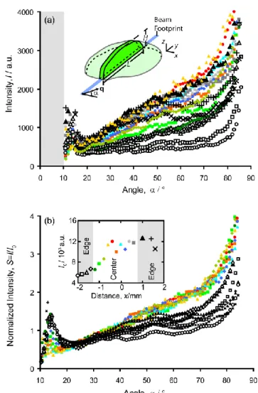
Fig. 3 Intensity I diffracted by a single droplet as a function of the
rotation angle . Different symbols indicate different positions x of the beam on the sample (color symbols – droplet center x0, white and black symbols – outer regions). Shaded areas with <10° correspond to total
60
internal reflection of the beam in the droplet. (a) Scattering curves
The inset show the geometry of the droplet and footprint. (b) Normalized intensity S=I/I0, with I0=I(d and =20-40°. Inset: I0 as a
function of x.
65
interface above the disclinations does not change along y over distances much larger than d.† Therefore, linear domains are invariant along y and relatively 'rigid': varying d and h along the y direction requires interrupting the domain, whereas variations along x can be obtained by assembling domains
70
with different thicknesses (h and h' in Fig. 2a). Variations of h along x produced the modulation of height z observed in AFM images, which was very shallow compared to the size d of the domains (Fig. 1d). The modulation is too small to be due to a convolution effect between the AFM tip and the
75
interface,14 which implies that: (i) the modulation z of height for a single domain was z<<d, and (ii) the difference of thickness h between neighboring domains was h<<d. For simple geometrical reasons (see Fig. 2a) these conditions imply that domains have approximately the mirror symmetric
80
shape described in Fig. 2b: the thickness h is much larger than the distance d, in agreement with previous results,16 curvature walls v are almost vertical and located midway between
disclinations, and most cylindrical layers end on the walls rather than on the substrate. The shape of such domain in a xz cross section is uniquely determined by the aspect ratio h/d or, equivalently, by the angle defined in Fig. 2b, such that q is normal to the free interface for <<. Since h is larger
5
than d, the angle acos(d/2h) is expected to be large, approaching in the limit of d/h0.
Calling l the domain length along the y direction, optical and AFM images showed that both d and l decreased as the droplet thickness decreased going from the drop centre to the
10
edge (Fig. 1b). The decrease along y was concentrated at the edges: the central part of the droplet contained domains with large l and d, sometimes extending almost from one edge of the droplet to the opposite, whereas both l and d rapidly decreased in a narrow peripheral region around the edge
15
where rigid domains (with fixed d and h) frequently split into thinner and narrower domains. This shows that the droplet had a "pancake-like" thickness profile, i.e. constant over a large area surrounding the centre. Such profile is common for droplets of nematic liquid crystals that wet and spread on a
20
solid surface under hybrid planar/homeotropic anchoring conditions.20 In fact, optical micrographs of our droplets show that the overall droplet shape does not change at the nematic-SmA transition.
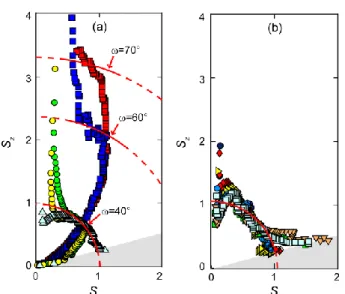
Figure 3a shows the scattering curves, I( obtained from
25
for a single, approximately circular droplet with maximum diameter 5 mm at different locations x of the incident beam. Curves obtainedin the range 0°were symmetric to those obtained for 90°<<180°, confirming that the domains had a mirror symmetry around curvature walls v (Fig. 2b). We
30
also measured the intensity I as a function of the angle between the diffraction plane and the domain axis, at several values of and a fixed value of the magnitude q = 0.2 Å-1.14 The I() curves always showed a narrow peak centered at =0, i.e., the intensity was maximum when the scattering vector q
35
was perpendicular to the disclinations. This confirms that the normal ('director') of the curved SmA layers rotates in the xz plane orthogonal to the disclinations (Fig. 2b). In the following, measurements of I as a function of were done at =0.
40
As the beam moved from the centre (defined as x0) towards an edge of the droplet, I( varied because the scattering volume changed (Fig. 3a, Inset). However, all curves could be reduced to a single master curve S(,x)=I(,x)/I0(x)in the interval 40°, when normalized
45
by the integrated intensity I0(x)=I(xd in this interval (Fig. 3b). Such master curve can be understood using the model of Fig. 2. A linear domain with dimensions d and land angle produces the scattered intensity =klf(d, where k is a constant and f()d is the distance of the disclination from
50
the domain boundaries (curvature walls and free interface) along the direction of the scattering vector q()The function f( is a shape factor, identical for all domains with the same shape (i.e., same , and closely reproduces the shape of the domain boundaries when represented in polar coordinates
55
fx=fcos and fz=fcos (Fig. 2c). The polar plot consists of an arc of circle for <<corresponding to the free
Fig. 4 Polar plots of the normalized intensity S() of Fig. 3, with
coordinates Sx=Scos and Sz=Ssin and the same meaning of the
symbols. (a) Droplet centre (x0). (b) Droplet edge. The curved line is an
60
arc of circle.
interface, connected trough inflection points to two vertical lines for < and corresponding to vertical curvature walls. In an assembly of domains, the total intensity
65
I)i=iniaifi depends on the number ni of domains with the same shape located in the footprint and on the area ai=lidi of their bases on the substrate. When the angle becomes smaller than the smallest i of the array, fi becomes independent from i and I,x)A(x)f(), where A(x) is the
70
area of the droplet in the footprint. Since the integral I0 of I calculated on any interval between 0 and min(i) is also proportional to A(x), the normalized curve S=I/I0 in this interval is independent from A(x) and x: S=f(). Experimentally, the plot of I0 as a function of x (Fig. 3b, Inset)
75
shows a plateau near the droplet centre where the intersection of the beam footprint with the droplet (area A) is maximum. The presence of a master curve for confirms the isomorphism of the linear domains at small angles, but its shape shows that the model of Fig. 2 does not correctly
80
predict the shape of the domain boundaries. At small angles, S() decreases more rapidly than expected and experimental polar plots of S() are not vertical, but highly curved (Fig. 4). According to the model, the intensity at small angles is due to the end portions of cylinders, close to a vertical orientation,
85
which end either on the mica surface or the vertical curvature wall v (Fig. 2b). Clearly, these portions of the cylinders are missing from the domain and a new domain structure must be considered near the substrate.
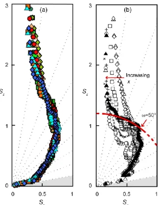
Fig. 5 (a) Polar plot of the normalized intensity S obtained from strips of
droplets aligned along y, at various positions x of the beam. Squares, circles and triangles denote respectively thick, thin and very thin strips. (b) Scattering from a single very thin droplet.
5
On the other hand, the results obtained for large angles, 40°<can be explained without changing the domain structure near the free interface, by introducing a distribution of sizes d, h and l and angles for the domains falling in the footprint. The normalized intensity S(x,) for large
10
depended on the position x of the beam. For a fixed S was almost constant with x near the droplet centre (-0.5 mm<x<1 mm) (Fig. 4a), and decreased as the beam moved towards the edges (x<-0.5 and x>1) (Fig. 4b) indicating that the main parameter influencing I) was the film thickness. As x
15
moved towards the edge, S became increasingly similar to the arc of circle predicted for the range <<, with an inflection point near 50° (Fig. 4b). To explain this behaviour, one should consider that the thickness H(x) and diameter L(x) of the droplet in the footprint decreased as the
20
beam moved towards the edges (Fig. 3a, Inset). For a given value of x, the thickness of the domains in the footprint was disperse in the range h[0,H]. Since a priori depends on h,16 was also more dispersed at the drop centre than at the edges. Therefore, the arc of circles observed near the edges
25
were due to domains having withlittle dispersion. Polar plots obtained at the centre were due to the combination of domains with a large dispersion of so that the normalized intensity S was the combination of arcs of circle differing by radius and angles of aperture. At the drop centre,
30
polar plots did not show any inflection point, which suggests that was dispersed in a wide range of interval extending up to 7S was almost independent from x at the centre of the droplet due its pancake-like shape: the maximum thickness H and thickness profile were almost uniform at the drop centre.
35
The influence of thin peripheral domains was reduced in experiments done on strips of droplets elongated along the y direction, which allowed the development of much longer
40
flattened central domains with almost uniform value of h. For large polar plots of S resembled arcs of circle with a single value of (Fig. 5a). The value appeared to increase with h as
45
predicted by earlier models16: from 40° for thin regionsto>60° for thick regions. This increase of with h did not affect the polar plots of S at small , which showed the same lack of intensity discussed above, due to missing portions of the cylindrical layers near the surface.
50
The behaviour at small changed for very thin films of 8CB. In the curves obtained for very thin strips of droplets, the arc of circle appeared to continue into the region of internal reflection <10°, without any inflection point. We obtained the same results with a single droplet prepared on
55
purpose to be very thin (small initial volume, long spreading time) (Fig. 5b). This indicates that decreased below 10° and the domain structure changed for very small thicknesses.
Fig. 6 Example of sub-domains containing (a) layers bent around a new
60
disclination (blue dot), and (b) flat horizontal layers. Domains of type (a) can be in contact with the substrate over an extended area if the disclination is tangent to the substrate. Domains of type (b) cannot touch the substrate without violating the planar anchoring condition. (c) Polar plot of the shape function f(), normalized by the value f(0), for the cases
65
of fig. (a) (dotted line) and (b) (solid line). The angle has the same meaning as in Fig. 2(b).
Discussion
The most interesting result in our measurements is that the
70
scattered intensity I decreases more rapidly than expected when the angle decreases. The deviation of I from the model curves (i.e., vertical lines in polar plots) is not limited to a particular range of angles, but continously increases as is decreased from the angle down to the minimum
75
measurable value of 10°. We first tried to explain the large deviation at small angles by replacing the end portions of the cylindrical layers, reaching the substrate with a vertical orientation and scattering at small angles, with a new sub-domain of 'misaligned' layers, located close to or intersecting
80
the surface. We considered both curved (Fig. 6a) and flat (plane) layers (Fig. 6b) and we imposed the following conditions:
(1) The domain shape and location comply with the overall mirror symmetry around vertical walls v observed in our
85
experiments. This condition is satisfied for a symmetric domain 'nested' along v.
(2) Layers inside the domain have a uniform (undeformed) thickness, while layer dilation is confined in a new curvature wall w that constitutes the domain boundary (Fig. 6a-b).7 (3) There is an equal number of layers ending on w on both sides. This conditions avoids dislocations and their high
5
energy of deformation.
(4) Layers always end with a vertical orientation on the substrate to satisfy the planar anchoring condition.
(5) Flat layers are almost horizontal (Fig. 6b) or almost vertical (Fig. 7), and the angle between the layer normal and
10
the substrate is respectively larger than 70° or smaller than 10°. Otherwise, flat layers would produce a strong peak of scattered intensity between 10° and 70°, which was never observed.
In the presence of curved or flat horizontal layers, the
15
calculated intensity was reduced in a limited interval of angles (Fig. 6c). The amplitude of the reduction and the interval of angles dependend on the type, location and extension of subdomain considered, but the intensity remained unchanged in the limit of → corresponding to vertical layers at the
20
substrate (Fig. 6c).
Fig. 7 Surface domains containing flat vertical layers, separated from the
cylindrical layers by curvature walls w. The cylinders are bent around
25
virtual disclination (blue dots) located at a depth p below the surface. To avoid dislocations, the vertical layer at a lateral distance x from the disclination meets the cylindrical layer of radius R=p+x on w. Layers meet on curvature walls v and w with disorientation angles v and w,
respectively.
30
Since we could not reproduce the observed overall deviation, i.e. at all angles, of the scattered intensity from the model prediction, we considered a global modification of the array structure: we placed the center of curvature of the cylindrical
35
layers on a virtual disclination, running at a depth p beneath the substrate and parallel to it (Fig. 7). A subdomain is now required at the substrate to prevent the cylindrical layers from reaching the substrate with a non-vertical orientation. Two hypotheses can be envisaged: either layers of the subdomain
40
are flat and vertical (Fig. 7), or they are curved. In the latter case different region of a single layer may have different radii and centers of curvature, spanning a virtual focal surface.18 We have considered the first case, because it is much simpler to analyse and reproduces all the main features observed in
45
the experimental scattering curves. We have also noticed that the inverse approach, i.e., starting from a subdomain of flat
vertical layers at the surface while excluding dislocation (point (3) above) on the curvature wall w (Fig. 7), necessarily leads to virtual disclinations or focal surfaces, which suggests
50
that the two aspects are closely related. To avoid dislocations, the shape of w must be such that the cylindrical layer with radius R=p+|x| centred on the virtual disclination must continue without interruption across w into the vertical layers that ends on the substrate at a lateral distance |x| from the
55
disclination. The number of layers on both sides of w is therefore |x|/a, where a is the thickness of a SmA layer.
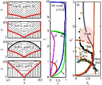
Fig. 8 (a-d) Shape of boundary wall w between flat vertical layers and the
cylindrical layers for various depths p of the virtual disclination and thickness h of the domain. (e) Polar plots of the shape function f(p/d)
60
for the examples (a-d). (f) The normalized intensity S obtained for single droplets and strips agree with model curves with fixed p/d=0.02. Dotted, dashed and solid lines correspond respectively to h/d=1.5, 2 and 10. For thick films, there is a dispersion of the h/d values (shaded area). A quarter of circle (dash-dot line) is compared to the data obtained for very thin
65
droplets and strips.
The height z of the w wall above the substrate is given by the intersection of the cylinder and vertical lines: z= (p2+2p|x|)½-p with 0<|x|<d/2. The maximum height is z*=z(p,d/2)d/2. Figs 8(a-d) show the curvature walls w between the surface region
70
with flat vertical layers and the cylindrical layers for different depths p of the disclination and thickness h of the linear domain. The overall shape of the linear domain is now specified by two aspect ratios, p/d and h/d. Domains with the same value of these parameters are isomorphic, and their
75
scattering curves I(will be proportional to the same shape function f(p/d, h/d) (Fig. 8e). In analogy with previous models, obtained for p=0, the h/d ratio can be replaced by the angle such that the scattering vector q is normal to the free interface for (Fig. 7). Notice that the polar plot of
80
the shape function f(p/d) is curved for all and does not reproduce the vertical shape of the v wall for whereas it still contains an arc of circle for . Polar plots of I() derived from this model are in good agreement with the results obtained for thick and thin droplets and strips, with a
85
constant value of p/d0.02 and different values of h/d (Fig. 8f). The maximum height of the wall w above the substrate can thus be calculated: z*(p=0.02d, x=d/2)0.12d<<h. Since d
ranges between 0.5 μm to 3.5 μm, the thickness of the surface region ranges between 60 nm and 400 nm which could hardly be revealed by polarizing or confocal optical microscopy. Nonetheless, the presence of such region has a profound effect on x-ray diffraction.
5
Experimentally, the shape function f(p/d) at small angles appears to be almost independent on the height h of the domains falling in the footprint, as demonstrated by Fig. 8f. Therefore, linear domains with different h had the same value of the parameter p/d: their surface regions had the
10
same shape. We call v the angle of disorientation between cylindrical layers that meet on the curvature wall v (Fig. 7). This angle is small at the free interface (v) and would reach a maximum value v at the solid substrate if flat vertical layers were not present. Instead, v reaches its
15
maximum value at a height z* from the substrate, where the vertical wall v splits into the w wall. The isomorphism of the surface region indicates that the splitting occurs at a specific angle of disorientation v=2atan(z*/d)0.92, rather than at a specific height z* (Fig. 7). It is well known21 that the energy
20
per unit area of a curvature wall rapidly increases with v, approximately scaling as v2 for vFor this reason, curvature walls are unstable and are usually replaced by a set of focal conic domains. Such 2D curved textures appear to be incompatible with the strong unidirectional planar anchoring
25
imposed by the crystalline substrate, and require a high energy to be nucleated in thin films.22 Instead, on mica the portion of the v wall with the highest energy (0.92 < v) is replaced by a couple of curvature walls w where cylindrical layers and flat vertical layers meet with smaller disorientation angles,
30
w< (Fig. 7). The energy per surface area on w is thereby greatly reduced. This should compensate the energy cost of replacing the small area lz*= 0.12ld of the removed portion of the v wall with the large area of the w walls, l(z*2+d2)½ ld . Moreover, replacing the disclination and the surrounding
35
cylinders with flat layers removes both the core energy of the disclination and the surrounding region with the highest density of curvature energy (due to small cylinders)16. The presence of virtual disclinations in 8CB/mica samples is a manifestation of the complex interaction of SmA defects
40
with solid substrates, still incompletely understood. On molybdenite, the interaction leads to formation of flattened hemi-cylinders and rotating grain boundaries, instead of virtual disclinations.9, 14 The difference with mica is likely due to differences in SmA/substrate interaction and nanoscale
45
structure of the interface: 8CB molecules adsorbed on molybdenite are strongly anchored in a planar and highly ordered lattice,23 whereas molecules adsorbed on mica show a distribution of orientations.19 The interaction between defects and substrate can take place through an evolution of the
50
curvature elastic constant and compression modulus of the SmA close to the substrate, where the local order parameter may increase or decrease from the bulk value.24 On molydbenite, a thin nematic layer has been evidenced in 8CB close to a molydbenite substrate,which may modify the elastic
55
constant K.15 In order to better understand the influence of anchoring strength, angular order and pretilt on the defect structure and interaction at the substrate, a study of non
-crystalline, more disordered surfaces becomes particularly interesting. Preliminary optical observations show that linear
60
arrays qualitatively similar to those obtained on mica and
molybdenite can also be obtained on rubbed polymers.
Therefore, the presence of a high degree of order at the substrate does not seem to be a necessary requirement for arrays to form.
65
Our results indicate that decreases as h decreases (Fig. 5), in agreement with previous calculations,16 while the S() curve at small angles remains the same ('thick' and 'thin' films in Fig. 8f) as expected for a fixed value of the parameter p/d (see curves 'b', 'c' and 'h' in Fig. 8e). However, as decreases,
70
the maximum height (d/2)tanof the vertical wall v above the substrate also decreases, approaching the maximum height z* of the w wall. When atan(z/d)13.5°, the v wall disappears and the top portion of the w wall become exposed to air, violating the homeotropic anchoring (Fig. 8c). At this
75
point, three scenarios are possible: (a) the ratio p/d (and therefore z*) decreases so that v does not disappear, (b) both w and v walls disappear (p/d=0, =0) leaving hemicylindrical domains centred on real disclinations, or (c) an anchoring transition occurs at the SmA/air or SmA/mica interface and
80
the layers become flat and aligned along the direction of strongest anchoring9, 16. Our measurements show indeed that the S() curves dramatically changes at small angles for very thin films (Fig. 8f), indicating that the ratio p/d changes and enters the region of internal reflection (<10°), possibly
85
becoming zero. Although we were not able to distinguish between case (a) and (b) due to the absence of data in this region, the curves show a distribution of layer orientation which allows us to exclude the case (c). Forthcoming scattering measurements in transmission at the ESRF, aimed
90
at determining the intensity variations for <10°, should clarify this point.
Conclusions
Large-area ordered arrays of linear defects appear in SmA
95
films deposited on crystalline surfaces are due to the combined effects of strong conflicting anchoring conditions and confinement to small film thicknesses. We anticipate this general result to be valid also for other types of substrates that induce a strong unidirectional planar anchoring, such as
100
rubbed polymers on glass or silica coatings obtained by oblique evarporation, which may be used to create even larger and more periodic arrays suitable for applications in nanoparticle assembly and soft lithography. Linear domains contain curvature walls and virtual singularities – seldom
105
observed in thermotropic SmA liquid crystals – and depend on the specific interaction of the SmA with the substrate. This interaction can have subtle effects, as demonstrates by the different defect arrangement of 8CB near the substrate of mica and molybdenite, in a thin surface region which could hardly
110
be revealed by optical means. Therefore, synchrotron x-ray diffraction is an important tool for the nanoscale study of defect-surface interaction.
Notes and references
† The height modulation over large distances along the y direction observed by AFM was mainly due to the non planar movement of the AFM scanner and tip relative to the free interface.
5
1 R. A. Segalman, Science, 2008, 321, 919.
2 I. Musevic, M. Skarabot, U. Tkalec, M. Ravnik and S. Zumer,
Science, 2006, 313, 954.
3 P. G. De Gennes and J. Prost, The Physics of Liquid Crystals, Oxford, 1974.
10
4 Y. H. Kim, D. K. Yoon, H. S. Jeong, J. H. Kim, E. K. Yoon and H. T. Jung, Adv Funct Mater, 2009, 19, 3008; Y. H. Kim, D. K. Yoon, H. S. Jeong and H. T. Jung, Soft Matter, 2010, 6, 1426.
5 D. K. Yoon, M. C. Choi, Y. H. Kim, M. W. Kim, O. D. Lavrentovich and H. T. Jung, Nature Materials, 2007, 6, 866.
15
6 R. Pratibha, W. Park and I. I. Smalyukh, J Appl Phys, 2010, 107, 063511.
7 M. Kléman, Points, lines and and walls in liquid crystals, magnetic
systems and various ordered systems, Wiley, New York, 1983.
8 M. Mitov, C. Portet, C. Bourgerette, E. Snoeck and M. Verelst,
20
Nature Materials, 2002, 1, 229.
9 J.-P. Michel, E. Lacaze and M. Goldmann, Phys Rev Lett, 2006, 96, 027803.
10 W. Guo and C. Bahr, Phys Rev E, 2009, 79, 011707.
11 J. B. Fournier, I. Dozov and G. Durand, Phys Rev A, 1990, 41, 2252;
25
C. Blanc and M. Kleman, Phys Rev E, 2000, 62, 6739; L. Z. Ruan, J. R. Sambles and I. W. Stewart, Phys Rev Lett, 2003, 91, 033901.
12 M. C. Choi, T. Pfohl, Z. Y. Wen, Y. L. Li, M. W. Kim, J. N. Israelachvili and C. R. Safinya, PNAS, 2004, 101, 17340; W. Guo, S. Herminghaus and C. Bahr, Langmuir, 2008, 24, 8174; W. Guo and C.
30
Bahr, Phys Rev E, 2009, 79, 061701.
13 V. Designolle, S. Herminghaus, T. Pfohl and C. Bahr, Langmuir, 2006, 22, 363.
14 J.-P. Michel, E. Lacaze, M. Alba, M. de Boissieu, M. Gailhanou and M. Goldmann, Phys Rev E, 2004, 70, 011709.
35
15 E. Lacaze, J. P. Michel, M. Alba and M. Goldmann, Phys Rev E, 2007, 76, 041702.
16 B. Zappone and E. Lacaze, Phys Rev E, 2008, 78, 061704. 17 H. Schuring, C. Thieme and R. Stannarius, Liq Cryst, 2001, 28, 241. 18 J. B. Fournier, Phys Rev Lett, 1993, 70, 1445.
40
19 B. Jerome and Y. R. Shen, Phys Rev E, 1993, 48, 4556. 20 P. G. DeGennes, Rev Mod Phys, 1985, 57, 827.
21 C. E. Williams and M. Kléman, J Phys (Colloques), 1975, 3, 315. 22 C. Blanc and M. Kleman, Eur Phys J E, 2001, 4, 241.
23 E. Lacaze, M. Alba, M. Goldmann, J. P. Michel and F. Rieutord, Eur
45
Phys J B, 2004, 39, 261
24 E. Lacaze, M. Alba, M. Goldmann, J. P. Michel and F. Rieutord, Eur
Phys J B, 2004, 39, 261.