HAL Id: jpa-00253508
https://hal.archives-ouvertes.fr/jpa-00253508
Submitted on 1 Jan 1994
HAL is a multi-disciplinary open access
archive for the deposit and dissemination of
sci-entific research documents, whether they are
pub-lished or not. The documents may come from
teaching and research institutions in France or
abroad, or from public or private research centers.
L’archive ouverte pluridisciplinaire HAL, est
destinée au dépôt et à la diffusion de documents
scientifiques de niveau recherche, publiés ou non,
émanant des établissements d’enseignement et de
recherche français ou étrangers, des laboratoires
publics ou privés.
Deep etch lithography at LURE-D.C.I. storage ring
S. Megtert, A. Labèque, Liu Zewen, H. Dexpert, R. Comès, F. Rousseaux, M.
Ravet, H. Launois, S. Ballandras, W. Daniau, et al.
To cite this version:
S. Megtert, A. Labèque, Liu Zewen, H. Dexpert, R. Comès, et al.. Deep etch lithography at
LURE-D.C.I. storage ring. Journal de Physique IV Proceedings, EDP Sciences, 1994, 04 (C9),
pp.C9-269-C9-272. �10.1051/jp4:1994947�. �jpa-00253508�
JOURNAL DE PHYSIQUE IV
Colloque C9, supplCment au Journal de Physique 111, Volume 4, novembre 1994
Deep etch lithography at LURE-D.C.I. storage ring
S. Megtert, A. Lab&que, Liu Zewen, H. Dexpert, R. Comks, F. Rousseaux*, M.F. Ravet*, H. Launois*, S. Ballandras*", W. Daniau*", S. Basrour*", M. Rouillay**, P. Blind*** and D. Hauden*"
Lahoratoire LURE, CNRS, Bdt. 2090, Universitk Paris-Sud, 91405 Orsay cedex, France
*
Lahoratoire de Microstructures et Micro&lectronique, L2MfCNRS, I96 Avenue Henri Ravera, 92225 Bagneux, France**
Lahoratoire LPMOICNRS32, Rue de l'ohsewatoire, 25000 Besancon, France***
Cetehor, 39 Rue de I'Ohservatoire, BP. 1145,25003 Besan~on, FranceAbstract : LIGA technique has proved to be a powerful tool for micro-fabrication mass production. French laboratories (LURE, L2M, LPMO) gathered to introduce this new technology at LURE facilities. In this paper are described the different steps of the deep etch lithography process including mask realization and first pseudo-tridimensional resist structures are shown.
I.
Introduction
In recent years, research and development on pseudo-tridimensional micro-machine technology went out from pure basic research to become a basic fabrication process for a large variety of micro- structures based on polymers, metals, ceramics and even glasses. The LIGA-technique has proved to be the most powerful tool in this respect [l]. It consists of a combination of deep X-Ray lithography, electroforming and molding (in German : uthografie, Wvanoformung, Abformung) and allows to get structures with a high aspect ratio (height over width up to about
loo),
lateral dimensions of a few microns if needed, size definition down to a fraction of one micron and freedom to design any structure shape without regard for further etching process. Since Germany started, other countries went into play like Japan, United States, Russia and now research institutes in Europe.As far as lithography is concerned it represents a widening of the well known lithography technique used for micro-electronic devices, the only differences being the structure height to built (up to one millimeter), the hard X-Rays (2-15 keV) provided by a synchrotron source and the suited mask technology using soft X-Rays synchrotron source
...
In France, LURE, L2M and LPMO laboratories share the necessary LIGA requirements, they also came into play end of 1992.
In this short paper we will restrict the presentation on the EIGA mask preparation and on the deep %-Ray lithography process. The latter is used to transfer the two dimensional mask pattern by shadow printing into thick resist to give rise to a pseudo-tridimensional object.
2.
X-Ray mask fabrication
X-Ray mask fabrication is one of the major concerns for LIGA process because it defines the "geometrical information" during the lithographic step. As the lithography is made in close proximity, X-Ray masks are "1%
".
This means that precision of the mask will be transfered in the image. The resolution, feature-size control, aspect-ratio of the resist pattern replications are mainly dependent on the mask characteristics, that is on the choice of the materials elements and on the severe control of their properties. An X-Ray mask consists in a transparent membrane supporting absorbing structures. In the case of deep etch lithography, the X-Ray spectral dismbution ranges between 0.05 and 0.6 nm, this means that the absorbing gold structures on mask are necessarily up to 10 pm-thick to absorb at least99 % of the beam distribution. This compelled specification on the absorber thickness drives the choice for the membrane properties (kind of material, thickness, residual stress,....). The whole compromise
JOURNAL DE PHYSIQUE IV
between absorber and membrane f n e s the mask contrast which is the relevant parameter for the lithographic results.
2.1 Materials
Membranes must meet a number of properties: large X-Ray transmission (> 50%), flatness, high mechanical stiffness, resistance to fracture, high thermal conductivity, radiation hardness, optical transparency ( ~ 5 0 % at 630 nm), roughness compatible with the size of the patterns. Among the different available materials, polycrystalline diamond is a good candidate because of its outstanding properties such as chemical inertness, highest thermal conductivity, low hydrogen content, low thermal expansion coefficient, highest nominal Young's modulus. All these properties guarantee a high stability under irradiation. Our first mask realizations have used two types of membranes. Silicon (Si) membranes 15-20 pm-thick which were obtained by classical chemical etching of a (100) Si wafer in KOH mixture and diamond membranes 2-5 pm. Diamond films were grown by MWCVD in a quartz bell jar low pressure chamber. Deposition parameters acting on nucleation and growth local conditions have been optimized to obtain thin films compatible with X-Ray membrane requests [3]. Membranes were obtained by removing the silicon substrate on 15-30 mm diameter circular windows. The optical transparency was optimized to 65% at 630 nm and the roughness was limited to 30 nm. Such roughness was prooved to be compatible with the growth of gold patterns with 100-200 nm lateral size
r21. L-a-
Absorber must be stress minimized to avoid local distorsions of the membrane. An additive process based on gold (Au) electrodeposition has been optimized using cyanid bath [3]. Gold structures were obtained with lateral sizes ranging from 100 pm down to 5 pm.
2.2 X-Ray mask processing
Two approaches for X-Ray mask processing have been tested. The first way consists to make the replication of an optical mask by contact UV lithography (UVL) in a thick Novolak photo-resist (12 pm) placed on top of a silicon substrate covered with the membrane material film. After the lithographic process, gold absorber is electrodeposited in the resist mold. The second way, consists to make directly a first "master mask" by e-beam lithography in thin polymethylmethacrylate (PMMA resist), 1 pm-thick, on top of a membrane followed by the same subsequent electroplating process. This "master mask" is then replicated in a thick PMMA layer (12 pm) by soft X-Ray proximity lithography (XRL) leading to a "daughter mask" appropriated to deep etch lithography. XRL replication is performed using the L2M lithography station implemented at Super-ACO storage ring (LITRE). ,--- - r -
The two methods are not quite equivalent concerning the ultimate limits of resolution and the aspect ratio of the absorber structures. With UVL replication process, the mask resolution is limited to a few microns (5 pm) and the gold feature sidewalls slope can range between 5' to 15'. With the XRL replication method, higher mask resolution can be obtained down to 0.5 pm (lateral size) with an excellent aspect ratio of rhe gold structures (sidewall slopes are practically vertical). Then depending on the specific needs of the LIGA object, one can choose one or the other way.
These masks have been tested on the synchrotron radiation of DC1 whose spectrum peaks at 0.25 nm. Replications have been performed in thick PMMA resist (500 pm) with a proximity gap of 100 pm.
3. Deep etch lithography.
A radiation sensitive polymer (resist) is used, the thickness of which is several hundred microns, as the transfer medium. Owing to PMMA's absorption properties, thickness, sensitivity and size definition, the best compromise is fulfilled with a highly collimated, high power, hard X-Ray synchrotron source.
The resist sensitivity may be defined independently of its thickness as the necessary absorbed dose (about 3 kJ/cm3 for a positive resist like PMMA) at the bottom of the resist layer (interface between resist and substrate) allowing its total dissolution in a given chemical bath.
A major problem is how "good" resist adhesion is per unit area (a few -2) with the metallic substrate (needed for further electroplating process) so that after chemical development the smallest
structures remain on it. Semi-empirical substrate chemical treatments (chemical bonding) and controlled roughness (mechanical inter-lock) were both used to achieve adhesion. For the smallest structures the effect of substrate fluorescence and backscattered photoelectrons also contribute to the lost of adhesion of the resist. Due to the relatively high sensitivity of PMMA to X-Rays in the range of 2
A,
low -Z-materials for which the fluorescence yield is as low as possible are prefered (Titanium instead of Copper for example).
Viscous 500 pm-thick resist are coated on the substrates and annealed in an oven for stress release after ambient temperature polymerisation.
For the pattern transfer, mask and resist are held close to each other (about 50 to 100 pm) in the sample stage of an X-Ray scanner and exposed to the filtered DCI-X-Ray beam.
After our first succesful tries with a simple exposure set up we measured all the relevant parameters to define the scanner we are now assembling. Due to the naturally collimated beam (0.22 mrad positrons divergency at D4 beam line), vertical source size (0=1.74 mm), photons divergency and source to sample distance (22 m), the vertical irradiation length is about 20 mm FWHh4. As the mask window may be much greater (up to 10 cm) one has to move mask and resist in front of the beam. In order to get homogeneous irradiation dose over the whole resist surface and to limit thermal load on the mask and resist, the sample stage is moved up and down at a speed of about 100 mm/s. The temperature of the mask and resist has to be stabilized within one degree to avoid pattem distortions (less than 0.1 pm). The perpendicularity between beam axis and sample stage must be kept within 0.1 mrad during the repetitive scans to maintain the accuracy of structure lateral dimensions within
+
0.1 pm. The resulting scanner is quite a big machine. Waiting for the delivery of our own system, we are actually sharing such a set up with colleagues from Germany (Institut for Microtechnique of Mainz, IMM) on the station D45 at LURE-DCI.The irradiation dose depends on a number of parameters (resist thickness, membrane material, gold absorber thickness, source characteristics, pattern height, filters, machine current and spectral distribution). These parameters are included in a software from which the exposure time is calculated. At DCI, a typical exposure time is about 50 mn for a 500 pm thick resist (50 mm field height) to get
3 Wcm3 at the bottom.
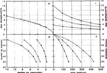
The last important step of the lithography process is the resist development. This step has to be carefully carried out to preserve the extremely precise and deep shadow printing achieved in the former step. The knowledge of the resist dissolution rate versus irradiation dose is the key of this process. Fig 1 represents the experimental way to construct this dissolution curve (IV) starting from the deposited dose at a given resist depth (curve I) and the etching depth for a given developing time (curve II).
develop in0 rats(um1min) resist depth(um)
Fig. 1 : deduced dissolution rate versus absorbed dose density in a thick resist (IV) as described in the text
.
C9-272 JOURNAL DE PHYSIQUE IV
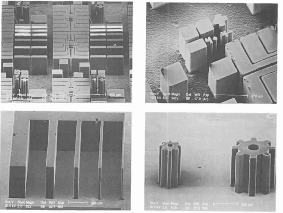
The whole described studies have been used to produce replications in PMMA. Some examples
are shown in the next electron scanning microscope photographs (Fig. 2). These examples illustrate the achieved resolution (down to 5 pm) and excellent aspect ratio (vertical sidewalls).
Fig. 2 : resist patterns replicated in proximity lithography at DCI-storage ring. Resist thickness was here about 300 pm.
References
[l] W.Ehrfeld and D. Miinchmeyer, Nuclear Instruments and Methods in Physics Research, A 303 (1991) 523-531.
[2] A.Gicque1, E. Anger, M.F.Ravet et al., Diamond and Related Materials, 2 (1993) p.417 [3] A.M.Haghiri-Gosnet, F.Rousseaux et al., J.Vac.Sci.Techno1. B8(6), NovPec 1990