The Development and Characterization of Kinematic Interfaces
for the Semiconductor Industry
by
John C. Alden
B.S. Mechanical Engineering Carnegie Mellon University, 1995
Submitted to the Department of Mechanical Engineering in Partial Fulfillment of the Requirements for the Degree of
Master of Science in Mechanical Engineering
at the
Massachusetts Institute of Technology February 1997
@ Massachusetts Institute of Technology
All rights reserved
Signature of Author
V Oiepaýment of Mechanical Engineering
January 24, 1997
Certified by ... ... ..
Alexander Slocum Alex & Brit d'Arbeloff Associate Professor of Mechanical Engineering Thesis Supervisor
Accepted by
Ain A. Sonin Chairman, Department Committee on Graduate Students
APR 1
APR 16 1997
LPPIRA91ESThe Development and Characterization of Kinematic Interfaces for the Semiconductor Industry
by John C. Alden
Submitted to the Department of Mechanical Engineering in Partial Fulfillment of the Requirements for the Degree of
Master of Science in Mechanical Engineering
ABSTRACT
An important stage of integrated circuit (IC) manufacturing is product testing. During this testing, a testhead must be interfaced with an IC handling device, and ultimately the IC. As more complex semiconductor devices are designed their pad pitch decreases making it more difficult to mechanically interface with the chip. As a result an extremely reliable, repeatable and rigid interface is required. Teradyne has developed a kinematic interface to meet the performance requirements of future interfaces.
Topics covered in this document include the mechanical performance characterization of the kinematic interface and the development of a possible standard interface performance characterization procedure. Life cycle evaluation of the kinematic interface components using PLC and PC control, and further developments of the kinematic interface including auto-planarization and a low-end mechanical version of the kinematic interface.
Thesis Supervisor-PAlexander Slocum
Table of Contents
CHAPTER 1: INTRODUCTION ...
FRONT END OF SEMICONDUCTOR MANUFACTURING ... ... 8...
THE NEED FOR AUTOMATIC TESTING ... ... ... 9
AUTOMATIC TESTING ... ... 11
AUTOMATIC TEST EQUIPMENT (ATE) ... ... ... ... 12
Testers ... ... ... 13
Peripheral Equipment... ... ... 15
Handling Equipment ... ... ... ... ... 16
Interfaces ... ... ... 17
SUMMARY OF AUTOMATIC TEST... 24
THESIS SUMMARY ... ... ... ... ... 25
THESIS CONTRIBUTION ... ... ... ... ... ... ... .... ... 25
THESIS STRUCTURE ... ... ... ... 26
CHAPTER 2: TERADYNE'S KINEMATIC INTERFACE...27
THE KINEMATIC COUPLING... 28
POTENTIAL BENEFITS OF THE KINEMATIC INTERFACE... 29
KINEMATIC INTERFACE FUNCTIONAL REQUIREMENTS ... ... 30
THE KINEMATIC MODULE... ... 33
The Gearbox ... ... ... ... ... ... 33
The Carriage... ... ... ... 33
The Z-adjust... ... ... ... ... 33
CONTROL ELECTRONICS ... ... ... ... ... 34
APPLICATION OF KINEMATIC INTERFACE ... ... ... 35
CHAPTER 3 : MECHANICAL TESTING OF THE KINEMATIC INTERFACE...36
M ECHANICAL TEST SITES ... ... 36
Motorola MOS 8 ... ... 36
Texas Instrum ents - Houston ... ... ... ... 39
MECHANICAL TESTING PLAN ... 40
M otorola M O S 8 ... ... .... ... ... ... ... 42
TI H ouston ... ... ... ... ... ... 43
MECHANICAL TESTING PROCEDURES ... ... ... . ... 43
Testhead Positional Repeatability ... ... ... ... 43
Probe Card Planarity -Repeatability ... 45
Interface Stiffness ... ... ... ... ... ... 47
Signal Integrity ... ... ... ... ... ... 49
Vibration Analysis ... ... . ... 51
RESULTS OF MECHANICAL TESTING ... 53
M otorola M O S 8 ... ... .... ... ... 53
Texas Instruments -Houston ... ... ... 59
CONCLUSIONS ABOUT MECHANICAL TESTING ... ... 61
INTERFACE CHARACTERIZATION PLAN ... 62
Sum m ary ... ... 65
LIFE-CYCLE TESTING ... ... ... 65
Sum m ary... ... .. ... 70
CHAPTER 4: FURTHER DEVELOPMENTS OF THE KINEMATIC INTERFACE...71
THE MINI-MODULE ... .. ... ... ... ... 71
D esign C onstraints ... ... 72
Design of the Mini-Module ... ... ... ... ... ... ... 74
Sum m ary ... .... .... ... . ... .... ... . ... 76
AUTO - PLANARIZATION ... ... ... ... ... ... 76
Error Budget - Feasibility ... . ... ... ... 77
Design Constraints ... ... 80
Design ... ... . . 80
Controls ... ... .. ... 82
Sum m ary... ... ... ... .... ... .. . ... 83
CHAPTER 5: SUMMARY AND CONCLUSIONS... 84
CHAPTER 6: APPENDIX ... 8 5 AVAILABLE RESULTS FROM THE MECHANICAL TESTING OF THE KINEMATIC, J-RING, AND INTEST INTERFACES ... ... ... ... 85
DETAIL DRAWINGS OF THE MINI-MODULE ... 88
DETAIL DRAWINGS OF THE AUTO-PLANARIZATION MECHANISM ... 95
List of Figures
Figure 1 : Processed Silicon W afer ... .. .. ... 9
Figure 2: Test Cell Layout ... ... 13
Figure 3: Photograph of a Tester ... ... .... 15
Figure 4: Prober ... ... .... 1 6 Figure 5: H andler ... 17
Figure 6: Testhead Interfacing with a Prober ... ... ... 18
Figure 7: Electrical Interface for Probe... ... 19
Figure 8: Probe Card and Needles . ... 19
Figure 9: Probe Needles at IC Bond Pads ... ... ... 20
Figure 10: J-Ring Interface ... ... ... 21
Figure 11: inTest Interface ... ... ... ... 22
Figure 12: Future Pad Count versus Year ... ... ... 24
Figure 13: The Kinematic Coupling ... ... 28
Figure 14: Ball and Groove Pair ... ... ... 29
Figure 15: The Latch Pin Mechanism... .... ... 32
Figure 16: Latch Pin and Groove ... ... 32
Figure 17: The Kinematic Module ... ... 34
Figure 18: A580 -KLA 1011 Application... . ... ... 37
Figure 19: A580 Testhead with Kinematic Modules ... ... ... 38
Figure 20: A580 -DeltaFlex Handler Application ... ... ... 39
Figure 21: Diagram of Physical Parameters that Ultimately Affect Yield ... 41
Figure 22: Probe Interface Structural Loop ... 41
Figure 23: Sensor Location for Testhead Repeatability Measurement ... ... 44
Figure 24: Probe Card Planarity Measurement Device ... ... 46
Figure 25: Forces Applied to the Testhead... ... .. .... .... ... 48
Figure 26: Signal Integrity Measurement Set Up ... ... 50
Figure 27: Vibrational Impulse Points... 52
Figure 28: Testhead Z-Repeatability ... .. ... ... 54
Figure 29: Probe Card Planarity Repeatability ... ... ... ... ... 55
Figure 30: Change in Probe Card Planarity Due to External Loads ... 56
Figure 31: Sample Signal Integrity Plot... ... 57
Figure 32: Deflection at Probe Card Due to Impulse Input... 5 8 Figure 33: Testhead Z-Repeatability ... 60
Figure 34: Deflection at Socket Due to Impulse Input... ... 61
Figure 35: Life Cycle Testing Fixture ... ... ... 66
Figure 36: Life Cycle Fixture Control Flow Diagram ... 67
Figure 37: The Second Life Cycle Fixture ... 68
Figure 38: The Fixture Control Box... . ... .... ... 69
Figure 39: Groove Locations of the Kinematic Interface ... 72
Figure 40: The Mini-Module ... 74
Figure 41: The Mini-Module Interface ... ... ...75
Figure 42: Prober/Testhead Model ... 78
Figure 43: Modules with Manual Z-Adjust and with Auto-Planarization ... 81
Figure 44: The Auto-Planarization Mechanism... ... 82
Chapter 1: Introduction
Chapter 1 is a brief introduction to the automatic testing of semiconductor products. The justification and need for semiconductor testing is discussed followed by a description of automatic test equipment. Testhead interfaces are introduced and their importance to semiconductor testing is presented.
Over the past few decades semiconductors have become a crucial component of modem society. To improve the "quality of life", semiconductor chips are used in a large number of systems including the automobile and in much simpler objects such as a toaster. Due to the demand by consumers for new electronic products, the number of applications and complexity of semiconductors are increasing at a rapid rate. Moore's .Law, developed in the 1960's by Gordon Moore, states that the number of transistors that semiconductor manufacturers can place on a chip doubles every year1. This was true until the 1970's, after which the rate slowed to a doubling of transistors every 18 months. Along with the increased application and complexity of semiconductors is a demand for increased reliability and decreased delivery time. For semiconductor manufacturers, "business success depends on getting more complex, but more reliable, products to market faster than ever before"2
Front End of Semiconductor Manufacturing
The manufacture of semiconductor components involves various production steps. At the front end of semiconductor manufacturing silicon wafer blanks are formed by
various stages of grinding and polishing. Layers of silicon nitride, silicon dioxide and photoresist are then deposited on the silicon blank. This prepared silicon wafer is
'G. Dan Hutcheson & Jerrry D. Hutcheson, "Technology and Economics in the Semiconductor Industry",
Scientific American, January 1996, p. 54
processed into multiple integrated circuits (IC's) by creating millions of transistors through repeated steps of photolithography, etching and doping. (Figure 1) Each processed silicon wafer can contain hundreds to thousands of IC's.
Figure 1 : Processed Silicon Wafer
Eventually, the IC's on the processed silicon wafer are separated. The individual IC's are glued to frames and placed into ceramic packages. The leads on the ceramic packages are connected to the bond pads of the individual IC, forming the chip common in everyday electronics.
The Need for Automatic Testing
An important stage of semiconductor manufacturing is product testing. Semiconductor manufacturers test the IC's in both the wafer form and the final package
form (chip). These two stages of testing are referred to as probe (wafer sort) and final test (chip test). The equipment used for this testing, automatic test equipment (ATE), is capital intensive, with typical prices in the million dollar range.
In addition to capital losses associated with equipment purchase, product testing also adds time, and hence cost, to semiconductor production without adding value. Since many IC's have prices below the ten dollar range the cost of test can be a significant portion of the manufacturing costs. If chips are cheap and testing and ATE is so expensive, how do semiconductor manufactures justify the cost of testing? The following excerpt from an article titled "Why Bother to Test?" addresses this question.
"... How do we know our devices are good if we don't test them? How do
we know our devices meet specifications if we don't test them first? Who wants to assemble a seven-layer PCB (printed circuit board) with over 200 ICs that haven't been tested? Naturally, each of these ICs has more than 250 pins each. Replacing even one or two of these devices might ruin the board. This could be very costly, not to mention delay shipping our products. ... To put even one bad part on a complex PCB is unacceptable. Rework costs or, worse yet, scrap and replacement costs are not good business. Good business is building only good products. So why bother to tests? Because we can't afford the cost of not testing." 3
Semiconductor testing is considered a cost avoidance strategy.
Semiconductor devices are tested for functionality and performance. Typical tests include checks for open circuits, shorts, and clock speed. Generally the ICs pass or fail the functionality and performance tests at different levels. In other words, testing is not always a strict pass/fail situation. For example, two devices on the same wafer may operate at a clock speed that is different from the device performance specification. The
device that does not operate at the specified speed is not thrown out, it is merely considered a lower speed device. This is precisely the situation with personal computer processors. Intel will manufacture one type of processor, for example a 120 MHz Pentium with Math Co-processor. When this device is tested, the chips that do not perform at 120 MHz are simply sold as 90 MHz, and those whose math co-processor does not work are sold as if they never had a math co-processor. This sort of strategy, where there is different levels of acceptable performance, is known as binning and sorting. Binning and sorting not only allow semiconductor manufactures to ensure the correct IC is being used or sold, but also allows the manufacturer to increase manufacturing yield (i.e. profit).
Automatic Testing
As mentioned, there are two stages of semiconductor device testing. The first stage is wafer probe. During probe the processed silicon wafer is placed in a handling device (prober) which presents the wafer to a testhead attached to a mainframe. The testhead is basically a large oscilloscope/signal analyzer that sends and receives signals to and from an IC and determines which individual IC is flawed. Probe test is an efficient means to test each individual IC because the IC's are still in wafer form, making it easy to
present each device to the testhead. Once tested the individual IC's are binned and sorted, and then packaged into chips.
The next stage of IC testing is final test. During final test the individual chips are presented to the testhead by a handling device (handler) . The devices are tested for functionality and performance, and are again binned and sorted. Final test is essential from an economics standpoint because it is the last check of a semiconductor device before it is mounted to a PCB. As mentioned before, the costs associated with mounting a non-functional device to a PCB is much greater than the cost of test. The functioning chips are
then mounted to printed circuit boards in various applications with a great deal of confidence that they meet the specifications.
To understand the need and benefit of IC testing, one obvious question to ask is why have two stages of testing. Again the answer lies in economics; the earlier in the process a fault is found, the less it costs.4 It is understood that it generally costs ten times
the amount to fix a fault at each subsequent production stage (i.e. packaging, mounting to PCB, integration into a system).5 The amount it costs to repair a fault in the packaged form of an IC versus repairing it in wafer form justifies probe test. If an IC does not pass the tests in wafer form then it will either be repaired, or will not be packaged. This saves money for the semiconductor manufacturer. Probe also provides a quality check on the "front end" wafer production. If an IC does not pass probe test the flaws are known to originate during wafer production. However, if an IC were only tested during final test there would be essentially no way to determine when flaws originated during production. It is because of probe and final test that a device is known to work and meet specifications before it is mounted to a PCB.
Automatic Test Equipment (ATE)
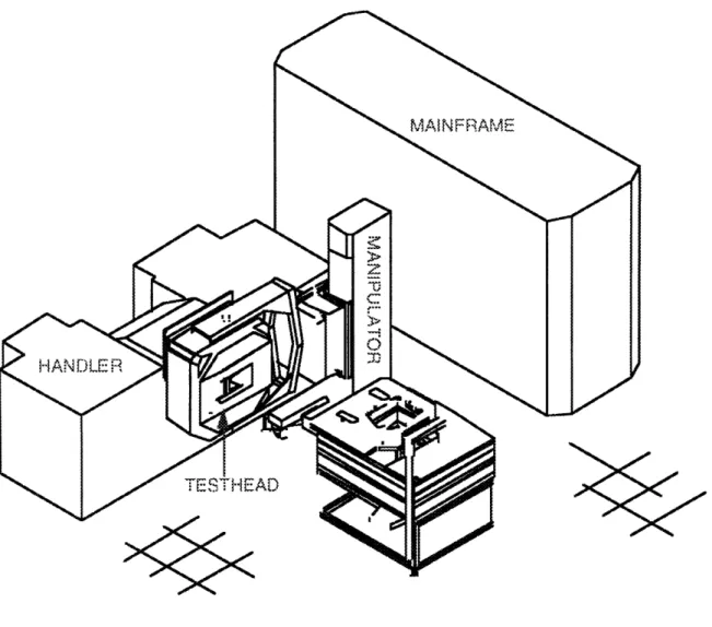
The automatic testing of semiconductors takes place in what are called test cells. A test floor will generally have a number of test cells, each of which contain the necessary equipment to test IC's in either the wafer or chip form. Test cells generally contain a tester (mainframe and testhead), a handling device (prober or handler), an interface, and a cable bundle and testhead manipulator. Below is a layout of a typical test cell. (Figure 2)
4 Brendan Davis, The Economics of Automatic Testing (London:McGraw Hill, 1982), p. 1
Figure 2: Test Cell Layout
Testers
ATE for electronics had its genesis over two decades ago. While archaic by today's standards, ATE of yesterday had the same function and general "architecture" of today's equipment. One of the first automated testers was a diode tester. The diode tester sent a signal to a diode and measured its performance. Depending on the measured output, the diode either passed or failed and was sorted accordingly. When one diode was finished testing a new one was interfaced with the tester and the process continued. Today's testers evaluate semiconductors in basically the same manner, albeit much faster and more sophisticated. A modem tester is a system that can send very accurate signals to the bond pads (bond pads, or pads, are the "input-output ports" of the semiconductor) of the 13
semiconductor device while measuring the output of some other pads on the same device. Depending on the measured value of the output the device is binned and sorted. After one device has completed testing a new device undergoes the same tests, a steady stream of devices are tested in this manner.
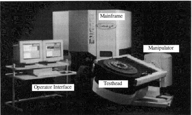
To minimize power consumption and time to test it is necessary to place the driving and receiving circuitry as close to the semiconductor device as possible. As a result, the tester is divided into the mainframe and testhead, making it possible to place the driving and receiving circuitry close to the device under test (DUT).(Figure 3) The mainframe is an electronic cabinet that contains the data processing circuitry which determines which signals to send and when, while at the same time measuring the output at the IC. The mainframe then compares the measured output with the expected output to determine if the IC has passed or failed a given test. The testhead contains the electronics required to generate, send, receive and measure signals to and from the IC. The electronics of the testhead include very accurate power supplies, function generators, and line drivers. By placing the driving and receiving electronics in the testhead, power consumption and time of test are minimized.
Figure 3: Photograph of a Tester
Peripheral Equipment
Along with the testhead and mainframe, most test cells contain peripheral
equipment, which may include a testhead manipulator, a cable bundle, and an operator interface computer. The cable bundle contains several cables required to connect the testhead to the mainframe. Because most of the cables of the bundle are shielded or twisted
pair, the cable bundle is extremely heavy (about 25 pounds per linear foot) and
cumbersome. To move the testhead and the cable bundle, and position them in various orientations a manipulator is used. The manipulator is basically a "fork lift" type device capable of supporting the weight of the testhead (often greater than 500 lbs) and managing the cable bundle. The operator interface computer allows a technician or engineer to control the tester and write the programs necessary to test the IC's.
Handling Equipment
To present the IC's to the testhead, handling equipment is used. In probe and final test distinctly different types of IC handling equipment is used. During probe test, a prober is used to position the processed silicon wafer with respect to the testhead. (Figure 4) By stepping its chuck (wafer handling surface) in the X and Y directions, the prober can position each IC on the wafer beneath the testhead for testing. Once all of the IC's on the entire wafer are tested, the tested wafer is removed from the chuck, an untested wafer is placed on the chuck, and the testing continues.
Figure 4: Prober
A device called a handler is used for final test. (Figure 5) The handler presents packaged IC's (chips) to the testhead for testing. Unlike the prober, a handler must present the chips to the testhead individually. The chips are plugged into a socket that is connected to the testhead. Once the chip is tested, it is removed from the socket and a new chip is plugged in for testing. This process continues in a steady stream of devices to be tested.
Figure 5: Handler
Interfaces
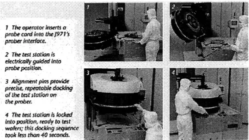
In order to test IC's, the main components of the test cell, the tester and handling device, are connected together using a device known as an interface. (Figure 6) The interface provides the mechanical link between the testhead and the handler or prober, while at the same time providing the electrical connection between the device under test and the testhead. While not the most expensive component of a test cell, the interface is often the most critical. The interface is the only link between the tester and the IC, and if the interface does not function properly, the entire test cell will be useless. Without an interface there is no way to test the IC's within the prober or handler.
I The opnr probe cord prober inter 2 The test j dectrkkaly probe positi 3 AMignmnei preCike, repi ofthe testsI theprober. 4 The tests Into poSlloi wofers; this took les th(x
Figure 6: Testhead Interfacing with a Prober
In general, the testhead interface consists of two main components, the mechanical interface which connects the testhead to the handler/prober, and the electrical interface which provides the signal delivery path between the testhead and the IC. The electrical interface consists of an array of conductive elements (pogo needles a.k.a. spring pins) which interact with various printed circuit boards.
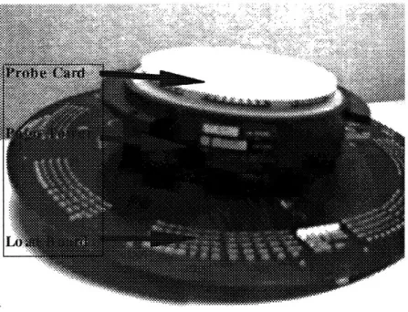
For probe, the three main components of most electrical interfaces are the probe card, pogo tower and load board (or dib).(Figure 7) The electrical interface brings the test signals from the pogo needles of the testhead down to the delicate tungsten probe needles of the probe card.(Figure 8) The probe card needles (probe needles) make contact with IC's at their bond pads.(Figure 9) Typical bond pads are .003"X.003" in area and are spaced about .003" inches apart. Due the small size and spacing of the bond pads, it is important that the probe needles be positioned accurately (i.e. planar with DUT), and repeatably.
Figure 7: Electrical Interface for Probe
Figure 8: Probe Card and Needles
··.:: :~:·:j::·-.·:~ :..:iii ,:::::: ::':: :·:·: : i:j:j:: lil:::~:~:i.-~i·:.ii~I i:i:::1 · :·:·:··.:.:.::-.··:·:-:·. :·:i: ·:·::·:·:-:·:·2::::,:·:·
Probe Card
Probe Needles
The Wafer
Figure 9: Probe Needles at IC Bond Pads
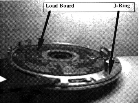
For final test the electrical interface is somewhat simpler and consists only of a load board. The load board for final test contains a socket, into which the chips to be tested are plugged. This allows the test signals to be guided from the testhead to the leads of the chip.
The second half of a testhead interface, the mechanical interface, must connect the testhead to the handler or prober, maintain electrical contact between the testhead and the load board, and must position the probe card, or device socket, and ensure its planarity with respect to device under test (DUT). Functionally, the mechanical interface must first align the testhead with the prober/handler, and with the load board, and then pull the testhead and the handling device together with a large enough force (about 300 lbs) to ensure the hundreds of pogo needles of the testhead are compressed. The interface must align the needles on the testhead to the load board within a window of about +/- 0.020". If the pogo needles do not fall within this window, the signal path between the testhead and DUT will not be closed and the test will fail. The alignment of the testhead is also important to ensure the probe card, or socket, is in position and in plane with the DUT. If there is misalignment of the testhead the probe card, or socket, will not be planar with the DUT which can lead to damage of the DUT or cause failed tests.
Due to the diversity of test equipment the design of interfaces tends to be application specific. As a result, there are dozens of mechanical interfaces in the semiconductor
industry. The majority of these interfaces operate via a "breach lock" or multi-point alignment and pull down mechanism. An example of a "breach lock" mechanism is the j-ring interface.(Figure 10) The j-j-ring interface uses a series of ramps and cam followers (located on the testhead) to pull the testhead to the handling device. Two to four alignment pins are used to align the testhead to the handler/prober and load board. The j-ring interface is shown below.
Figure 10: J-Ring Interface
Another common mechanical interface is the inTest interface.(Figure 11) The inTest interface uses from two to four cone and hole pairs and a system of cams and cam followers to align and pull the testhead to the handling device and load board. The inTest interface is shown below.
Figure 11: inTest Interface
As mentioned above, the mechanical interface needs to be rigid and repeatable. Repeatability of the interface ensures pin pad contact at the load board and, for probe, planarity of the probe card every time the testhead is docked (docked it the term used for connecting the testhead to the handling device). Rigidity of the mechanical interface will minimize testhead movement while subjected to external forces. This, in turn, will maintain the signal path when external forces are applied.
While the j-ring, inTest, and most other mechanical interfaces perform their function adequately, there are problems associated with them. It is known qualitatively that most interfaces are not repeatable or rigid. The lack of repeatability stems from the fact that most interfaces are either over or under constrained. The j-ring interface, for example, is under constrained, allowing the testhead to float while docking and provides no final alignment mechanism. This results in non-repeatability. The inTest interface, on
the other hand, is over constrained which causes non-repeatability. In order for a testhead to be docked repeatably, the interface must be perfectly constrained (i.e. six constraints for six degrees of freedom). The lack of rigidity with the inTest and j-ring interfaces is due to
the fact that the interfaces will flex considerably when subjected to a load. This flexing of the interface will result in movement of the testhead.
Along with mechanical performance problems (repeatability and rigidity), the j-ring, inTest, and a number of other interfaces require a semi-skilled operator to use them. The operator must be trained in the use of the interface, and to be effective must have considerable experience using the interface. An inexperienced, or untrained, operator of an interface will, most often, not be able to dock the head properly (i.e. rigidly and in the correct alignment) without several attempts. Ideally the interface would not rely on the skill of the operator for proper use.
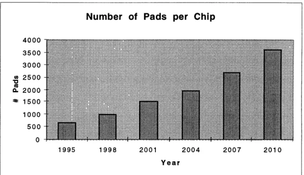
As more complex semiconductor devices are designed an extremely reliable, repeatable and rigid interface will be required to test them. This is because as devices become more complex, the number of bond pads, and hence chip leads increase. Figure 12 shows the predicted number of pads per die site for ASIC's (Application Specific Integrated Circuits) by the year 2010. Along with the increase in the number of pads comes a decrease in the spacing, or pitch, of the pads. By the year 2010 the pitch of the pads will have decreased from the current value of 75 ýpm (.003 inch) to 50 gtm (.002 inch).6 As the number of pads increases and their spacing decreases, it becomes more critical that testhead interfaces be able to repeatably locate the probe card or device socket.
Number of Pads per Chip
Figure 12: Future Pad Count versus Year7
Summary of Automatic Test
The automatic testing of semiconductors, while capital intensive, is a necessary cost avoidance strategy used in semiconductor production. Automatic testing is performed by automatic test equipment (ATE) on test floors in units called test cells. Test cells generally consist of a tester (mainframe and testhead), a handling device (prober or handler), a manipulator and cable bundle, and an interface. While not the most costly, the interface is often the most crucial element of a test cell. The interface mechanically connects the testhead to the handling device and electrically links the testhead to the IC under test. The mechanical portion of the testhead must rigidly and repeatably couple the testhead to the handler or prober. If either portion of the interface, mechanical or electrical, does not function properly then testing the IC's in the handling device is not possible.
7 The National Technology Roadmap for Semiconductors, 1994, p. 41
4000 3500 3000 0 2500 0. 2000 * 1500 1000 500 0 1995 1998 2001 2004 2007 2010 Year
To meet the performance requirements of future interfaces, Teradyne has developed a Kinematic Interface. In short the kinematic interface is a three ball-three groove system which results in an extremely rigid and repeatable interface. This document is focused on the kinematic interface developed at Teradyne.
Thesis Summary
This thesis, submitted as part of the requirements for completion of a S.M. in Mechanical Engineering, will focus on the development and characterization of Teradyne's kinematic interface. Topics covered in this document will include a description of the kinematic interface, mechanical performance characterization of the kinematic interface and the development of a possible standard testhead interface performance evaluation procedure, life cycle evaluation of the kinematic interface components using PLC and PC control, and further developments of the kinematic interface including auto-planarization and a low-end mechanical version of the kinematic interface.
Thesis Contribution
The work presented in this document was completed over a one year period while the author was employed by Teradyne. While not all of the time employed at Teradyne was spent on the work of this thesis, the author learned a great deal about the semiconductor industry. The author completed the following as part of the work included in this document.
* Design aspects of the kinematic interface
* Mechanical test plan and mechanical testing of the j-ring, inTest and kinematic interfaces.
* Conceptual development of the standard interface characterization plan. * Design and development of the kinematic module life cycle testing fixtures
* Design and development of the "mini-module"
* Design and development of the auto-planarization unit
Thesis Structure
The remainder of this thesis is structured as follows. Chapter 2: Teradyne's Kinematic Interface
Chapter 2 serves as a brief introduction to the kinematic interface. Chapter 3: Mechanical Testing of the Kinematic Interface
Chapter 3 presents the mechanical testing of the kinematic interface and its components.
Chapter 4: Further Developments of the Kinematic Interface
Chapter 4 describes further developments of the kinematic interface. These include the mini-module and auto-planarization.
Chapter 5: Conclusion
Chapter 2: Teradyne's Kinematic Interface
Chapter 2 serves as a brief introduction to the kinematic interface. Its purpose is to provide background information for topics developed later in this document. In this section the basis of the kinematic interface, the kinematic coupling, is described. After a discussion of the potential benefits of a kinematic interface the functional requirements and design of
Teradyne's kinematic interface are discussed. Although the author contributed to the detailed design of the kinematic interface, for clarity, the details of the design are not mentioned. The electronics required to control the kinematic interface, along with the application of the kinematic
interface, are also mentioned briefly.
A rigid and repeatable interface is important to maintain the testhead to device signal path. There are a number of testhead interfaces in existence that exhibit varying levels of stiffness and repeatability. The need for a more repeatable, stiffer interface is increasing as more complex semiconductor devices are produced. To meet the need of future interfaces, Teradyne has developed the kinematic interface. The kinematic interface is an interface that, simply stated, uses three balls and three grooves to provide a more repeatable, stiffer testhead to prober/handler coupling.(Figure 13)
Figure 13: The Kinematic Coupling
The Kinematic Coupling
The ball and groove coupling of the kinematic interface is based upon the kinematic coupling developed to obtain high repeatability for fixtures. Kinematic couplings are deterministic: in other words they only make contact at a number of points equal to the number of degrees of freedom they are to restrain.8 Being deterministic, kinematic
couplings are immune to the results of an over constrained system and hence are extremely repeatable.
In order to position an object in six degrees of freedom, the kinematic coupling needs six points of contact. One way to accomplish this is by using three grooves and three balls. Each ball-groove pair provides exactly two contact points, three sets of the ball-groove pairs results in the six points of contact required to perfectly constrain the object.(Figure 14) To provide a rigid coupling the kinematic coupling can be preloaded, or in other words a force pushes the ball into the groove. Using the concept of a preloaded kinematic coupling, Teradyne developed the kinematic interface.
Figure 14: Ball and Groove Pair
Potential Benefits of the Kinematic Interface
A kinematic coupling offers three main benefits: repeatability, rigidity, and ease of
use. The experience using kinematic couplings for fixturing attests to their high repeatability. If the kinematic coupling is preloaded then it will take a force equal to the preload to separate the ball groove pairs. In other words, the preload of the kinematic coupling makes it rigid. Since the kinematic coupling is perfectly constrained, (i.e. six points of contact for six degrees of freedom) it is easy to use. This is because there is no binding when mating two objects using a kinematic coupling. Based on these benefits, a kinematic coupling used to connect a testhead to a handler or prober could provide a rigid and repeatable interface that is easy to use.
Kinematic Interface Functional Requirements
There were a number of functional requirements that had to be met in the design of the kinematic interface. These requirements shaped the final form of the kinematic interface. Some of the functional requirements are listed below.
* Rigidly dock the testhead: To rigidly dock the testhead, the kinematic interface needs to apply a preload force.
* Repeatably dock the testhead: The mating of the three ball and groove pairs ensures a repeatable dock.
* Avoid damage to the pogo pins of the electrical interface: To avoid damage to the pogo pins, the kinematic interface must roughly align the testhead before fully docked (or when the balls and grooves make contact).
* Uniformly compress the pogo pins: A coupling force must be applied by the interface to ensure the hundreds of pogo pins of the electrical interface are compressed.
* Report the status of the dock: The kinematic interface should be "intelligent". If a dock has failed (i.e. not preloaded, or not aligned), then it should report this to the operator.
* Must be able to planarize the testhead: The operator needs to be able to planarize the testhead with respect to the handling device. Ideally this would take place via the kinematic interface
The Kinematic Interface Basics
Based on the concept of the kinematic coupling, Teradyne's kinematic interface employs three grooves and three balls. Three balls are mounted on the testhead while the three mating grooves are mounted on the prober or handler. A preload mechanism is
combined with the balls into units called the kinematic modules. The two main functions of the kinematic interface are dock and undock, or coupled and uncoupled. At full dock, the modules provide a preload force and pull the balls to the grooves thereby providing the mechanical coupling of the testhead to the prober/handler. At full undock the balls are free from the groove and the testhead can be removed from the handler/prober.
The main mechanism of the kinematic module is a latch pin which interfaces with the coupling groove. Basically, the latch pin of the dock module can "mate" with the k-dock groove in a matter that is similar to a socket and ratchet set. A set of four small steel balls, within the latch pin, can extend beyond the latch pin and cause interference with the groove, allowing a preload force to be applied.(Figures 15 and 16) The preload force pulls the balls and grooves together creating a rigid testhead to handler/prober connection. When a release force is applied, the small steel balls retract within the latch pin and allow separation of the latch pin, and hence the ball, from the groove. The latch pin/ball/groove interaction is the basic function of the kinematic interface.
I
PRELOAD FORCE
rOlOm\VF
DOCK
Figure 15: The Latch Pin Mechanism
Figure 16: Latch Pin and Groove
UNDOCK
The Kinematic Module
To meet the functional requirements the relatively simple latch pin, ball, groove mechanism has evolved into a relatively complex system of motors, sensors, and electronics. The latch pin and ball are combined with a d-c motor, gearbox, a number of sensors to form a kinematic module. There are three main components of the modules: the gearbox, the carriage, and the z-adjuster.
The Gearbox
The gearbox contains most of the functionality of the kinematic module. It contains the ball, the latch pin, a d-c motor, appropriate gearing to drive the latch pin and three sensors to determine the state of the module. The d-c motor and gearbox are designed to provide in excess of 300 lbs of preload force per module.
The Carriage
The carriage is two plates connected by a set of crossed roller bearings. The crossed roller bearings allow the plates to move relative to each other which allows the user to planarize the testhead by adjusting the relative position between the two plates on each module. The gearbox and z-adjust are mounted to the carriage which is then mounted to the testhead.
The Z-adjust
The z-adjust is a manual adjustment mechanisms that controls the position of the two plates of the carriage relative to each other. By turning the z-adjust mechanism of each module a certain amount, the testhead can be planarized with respect to a reference surface. The carriage, gearbox, and z-adjust combine to form the kinematic module.(Figure 17) Three kinematic modules and three grooves along with control electronics make up Teradyne's kinematic interface.
Figure 17: The Kinematic Module
Control Electronics
The control electronics of the kinematic interface drive the dc motor of the modules, and use the output of the three sensors of each module to determine the state of the interface. The three states of the interface are docked, undocked and ready to dock. An operator can go to each of these states by pushing one of two buttons on a control pendant. By pushing dock the control electronics will drive the motors of the modules to the docked position. Similarly, by pressing undock the control electronics will drive the motors to the undock position or, depending on the state of the modules, to the ready to dock position. There is a fairly complex state machine that keeps track of what state the interface is in and whether or not a requested action (dock or undock) can be performed. The state machine, along with the feedback from the module sensors allow the controller to determine if the dock was successful. This state machine is programmed and stored on an E-prom (erasable -programmable read only memory) which is integrated with a gate array and three motor controllers to control the modules of the kinematic interface.
Application of Kinematic Interface
The kinematic interface was designed specifically for integration into Teradyne's new series of testheads known as Catalyst, Magnum, and Marlin (a.k.a. the beta series testheads). Each of the beta series testheads have built-in mounting locations around their perimeter for the kinematic modules. While only three mounting locations are required for the kinematic interface, each testhead has six. This is to provide flexibility when integrating the kinematic interface with a specific prober or handler. This flexibility will allow the kinematic interface to be used with nearly any handler or prober. The possibility to be used with any handler or prober has the potential to make the kinematic interface an industry standard, which is clearly needed in the semiconductor industry.
"One item not shown on the Testing and Test Equipment roadmap is the need for standard mechanical/electrical interfaces between automatic probers or package handlers and test systems. At the present time, dozens of interfaces have been developed at great expense."9
The kinematic interface could easily become a standard interface for Teradyne testheads.
Summary
Teradyne developed the kinematic interface to meet the performance requirements of future interfaces. Based on the kinematic coupling, the kinematic interface can provide a rigid and repeatable interface that is easy to use. Due to the many functional requirements the kinematic interface has evolved from relatively simple mechanism into a fairly complex system of motors, sensors and electronics. Since Teradyne's new generation testheads have multiple kinematic module mounting locations the kinematic interface could become a standard testhead interface.
Chapter 3 : Mechanical Testing of the Kinematic Interface
Chapter 3 presents the mechanical testing of the kinematic interface and its components. A series of mechanical tests were developed, and applied, to quantify the mechanical performance of the kinematic interface, and the j-ring and inTest interfaces. The test sites, basis for the tests, and testing procedures and results are presented. A proposed standard interface characterization procedure, based on the interface mechanical testing, is then discussed. At the end of this chapter the life cycle testing of the kinematic module, as well as the design and development of the life cycle
fixtures, are presented.
To prove the concept of the kinematic interface and the benefits it offers, two test sites were chosen with the intent of using the kinematic interface on the sites' production floor. The kinematic interface was integrated with the A580 AMS (Advanced Mixed Signal) testhead, an older generation testhead, in both a probe and handler application. The kinematic interface was integrated with the A580 because Teradyne's new generation testheads (i.e. Catalyst, Magnum, Marlin) were not available at the time of the mechanical testing. With the kinematic interface installed at the test sites, various data was collected for the kinematic interface and the j-ring (Probe application) and inTest (handler application) interfaces. A number of mechanical tests were developed to quantify the mechanical attributes of each interface.
Mechanical Test Sites
Motorola MOS 8
At Motorola MOS 8, the kinematic interface was integrated with the A580 testhead to allow interfacing with a KLA 1011 prober.(Figures 18 and 19) Due to the lack of groove mounting locations on the prober head plate and because the modules can not be mounted directly to the A580 head, it was necessary to design mounting brackets for the
modules and support brackets for the grooves. As a result, this application was somewhat bulky and difficult to use. In future applications (i.e. Beta Series testheads) the modules will be mounted directly to the testhead and should provide better performance and easier use. The mechanical test application, however, was sufficient to prove the concept of the kinematic dock.
Bracket on Testhead
/
Module/
Bracket or
Texas Instruments -Houston
At Texas Instruments (TI) Houston the kinematic interface was integrated with the A580 testhead to allow interfacing with a DeltaFlex vertical plane, pick and place handler. (Figure 20) Due to the lack of groove mounting locations on the DeltaFlex plate and because the modules can not be mounted directly to the A580 head, it was necessary to design mounting brackets for the modules and extension plates for the grooves. As a result, this application was somewhat bulky and difficult to use. In future applications (i.e. Beta Series testheads) the modules will be mounted directly to the testhead and should provide better performance and easier use. The mechanical test application, however, was sufficient to prove the concept of the kinematic dock.
Module and
BracKei
",*
Lower F
Extensik
Mechanical Testing Plan
A mechanical test plan was developed for the prober application and subsequently
modified for mechanical testing of the handler application. The mechanical tests for the prober application were developed on the basis of physical parameters of a probe interface that ultimately affect yield. Figure 21 is a diagram of physical parameters of the testhead interface and how they map to product yield. For example, deflection and non-repeatability of the testhead can cause deflection of the load board (DIB) and testhead misalignment. As the effect of load board deflection and head misalignment are traced through the structural loop of the interface (Figure 22), the ultimate result is a loss of "pin to pad" contact and hence poor signal integrity and low yield. Based upon this type of analysis, various tests were developed that could be used to quantify the performance of an interface.
Figure 21: Diagram of Physical Parameters that Ultimately Affect Yield
Below is a list of possible tests, generated from the above figures, that could be performed to evaluate the mechanical performance of an interface.
* Probe Card Repeatability
* Determine probe needle position using downward looking camera * DIB deflection
* Iso-pin compression * Pogo-pin scrub
* Positional repeatability of testhead * Interface Stiffness
* Vibrational tests -impulse test
* Signal integrity
Not all of the above tests were performed. Probe needle location, DIB deflection, iso-pin compression, pogo-pin scrub were not measured because time constraints, lack of equipment, and the impracticality of the measurements. Below is a list of the mechanical tests that were performed at the mechanical test sites.
Motorola MOS 8
1. Testhead Repeatability: The positional repeatability of the testhead with respect to the prober was measured on a per dock basis.
2. Probe Card Planarity: The planarity of the probe card with respect to the prober chuck was measured on a per dock basis.
3. Interface Stiffness: External loads were applied to the testhead while it was docked and the resultant testhead movement and change in probe card planarity were measured.
4. Vibrational Analysis: The vibration at the probe card due to external impulse forces applied to the testhead, prober, and manipulator was measured.
5. Signal Integrity: The "signal integrity" was measured while external impulses were applied to the testhead, prober, and manipulator.
TI Houston
1. Testhead Repeatability: The positional repeatability of the testhead with respect to the handler was measured on a per dock basis.
2. Vibrational Analysis: The vibration at the handler socket due to external impulse forces applied to the testhead, handler, and manipulator was measured.
Although it was planned to perform signal integrity and stiffness tests at TI, it was not possible. The custom wired load board used for the signal integrity tests did not interface with TI's handler, and the handler docking plate was too compliant to be used as a reference surface for stiffness measurements (a separate metrology frame would have been required).
At each test site, the mechanical tests were performed on the kinematic interface and on the existing interface to provide a benchmark for performance comparison. At Motorola MOS 8 the existing interface is the J-Ring and at TI Houston the existing interface is the inTest plate.
Mechanical Testing Procedures
Testhead Positional Repeatability
Measurement devices were attached to the testhead using mounting fixtures and the measurement targets were attached to convenient locations on the prober or handler. Three other measurement devices were mounted to the prober or handler and touched off the testhead.(Figure 23) Every time the testhead was docked, the read-out of the measurement devices was recorded. This data was then compiled using a transformation matrix which calculated the change in testhead position after each dock.
73
zi
I r
Figure 23: Sensor Location for Testhead Repeatability Measurement
Equipment Used:
3 Sony Magnascales (linear measurement device) 3 Digital Indicators (linear measurement device) 3 Magnascale Targets
3 Magnascale Mounting Brackets 3 Indicator Stands
Probe Card Planarity -Repeatability
Probe card planarity was measured for the prober application. The planarity of the probe card with respect to the prober's chuck (wafer handling surface) was measured using a custom measurement device.(Figure 24) The planarity measurement device consists of a non-contact sensor mounted on a metal disk which is placed on the prober chuck, and a metal plate that mounts to the pogo tower, replacing the probe card. With the testhead docked, the prober chuck is stepped in x and y and the gap between the sensor face and the tower plate is recorded. By keeping track of the x and y position and gap at each location a planarity plot can be made. The components of the measurement fixture were not manufactured to precise geometric tolerances (i.e. flatness). This was unnecessary because the deviation of planarity of the probe card from an average position was of interest. Because of this, any errors in measurement caused by manufacturing were subtracted out. If a similar device was to be used for a "one dock" planarity measurement, the flatness of the components would have to be more precise, and three non-contact sensors would be needed.
To measure the repeatability of the probe card planarity, the testhead was docked thirty times, each time the planarity was recorded. Every fifth dock the load board-pogo tower-probe card assembly was moved to simulate changing the probe card.
Custom Me. Device Mea,
Between ChUCK ana
Probe Card
/
TOWER PLATE CHU PLA'Figure 24: Probe Card Planarity Measurement Device Equipment Used
Non-contact measurement probe (inductive or capacitive sensor) Tower Plate (sensor target mounted to pogo tower)
Interface Stiffness
The static stiffness of the interfaces was measured for the probe application. To quantify the static stiffness of the interfaces, loads were applied to the testhead while it was docked and the resultant movement of the testhead and change in probe card planarity were recorded. The testhead movement was measured using the same set-up as the testhead repeatability measurements, and the probe card planarity was measured the same as described above. Figure 25 is a diagram of where loads were applied to the testhead. A standard load of 40 lbs was used to simulate external forces such as someone leaning on the testhead, or changes in cable forces caused by cable bundle position.
Y
A rL..~AI Positive a NegativeZ
Positive Negativ(Figure 25: Forces Applied to the Testhead
Equipment Used
250 Lb. Load Cell
2 Nylon straps
3 Sony Magnascales (linear measurement device)
I _
i •
3 Digital Indicators (linear measurement device) 3 Magnascale Targets
3 Magnascale Mounting Brackets 3 Indicator Stands
1 Non-contact measurement probe (inductive or capacitive sensor) 1 Tower Plate (sensor target mounted to pogo tower)
1 Chuck Plate (plate to mount sensor to chuck)
Signal Integrity
When the mechanical test plan was developed, it was decided that the "tell all" measurement would be the variation in signal integrity caused by external forces and vibration. Based on this, a plan was developed to measure the signal integrity for the probe application. No method of measuring the signal integrity could be found so it was necessary to develop the following test procedure.
To obtain a measure of the signal integrity, a signal is sent through a custom wired iso-block (part of the testhead signal path) and load board This signal then travels through the pogo tower down to the probe card, an aluminized wafer completes the circuit. A dynamic signal analyzer is used supply a white noise signal through the iso-block-DIB-probe card circuit. The signal is measured across the iso-block-DIB-probe needles, as impulse forces are applied, and compared with the input signal. The coherence of the output to the input is calculated. If the signal integrity is "perfect" a coherence of one is calculated, the coherence will go to zero as noise is introduced to the system. (i.e. probe needles vibrating) Figure 26 is a sketch showing the experimental set up and electrical schematic.
DIB
minized Wafer
Measured Iso-Block and Tower
Voltage
Applied Voltage Probe NeedlesProbe Needles
Figure 26: Signal Integrity Measurement Set Up
Equipment Used 1 Custom wired DIB 1 Custom wire Iso-block
1 Hewlett Packard 35670A Signal Analyzer 1 Digital Multi-meter
1 Probe Card
ff
1 Aluminized Wafer
1 PCB 3 pound Calibrated Sledge Hammer
Vibration Analysis
With the test head docked, impulse loads were applied to quantify the dynamic stiffness of each interface. A calibrated impulse hammer was used to apply the impulses, while a tri-axial accelerometer measured the level of vibration at the probe card for the probe application, and at the socket for the handler application. The testhead, prober/handler, and manipulator were struck with the impulse hammer to simulate different vibrational inputs. A dynamic signal analyzer was used to record and perform analysis of
the accelerometer data. Figure 27 is a diagram of the impact points for the KLA 10xx and DeltaFlex applications.
A - On Prober B - Up on Head Plate C - On Manipulator D - On Testhead E - Up on Iso-Carrier
IE
Hammer Trigger: A,B,C - 50 N D,E - 25 N SIGNAL INTEGRITY RED - 25N BLUE -12.5 N F A - On Testhead Tub B - On Iso-CarrierC - On Iso-Carrier (into page) D - On DeltaFlex plate (out of page) E - On DeltaFlex Plate
F - On DeltaFlex Plate
Hammer Trigger 10 N
Figure 27: Vibrational Impulse Points Equipment Used
1 Hewlett Packard 35670A Signal Analyzer
1 PCB Tri-ax Accelerometer
1 Accelerometer to Pogo Tower Mounting Plate
Results of Mechanical Testing
Motorola MOS 8
At MOS 8, the kinematic interface performed significantly better, mechanically, than the j-ring interface.
Testhead Repeatability
Testhead repeatability is an important attribute of an interface. Good repeatability leads to uniform iso-pin compression, which leads to uniform load board loading, and ultimately to consistent probe card planarity. In short, if a testhead is docked repeatably then probe card planarity will be maintained. Measurements of the probe card planarity (below) support this claim.
To quantify the positional repeatability of the testhead, the testhead was docked and undocked thirty times and its position, with respect to the prober, was measured each time. Figure 28 is a typical plot of the testhead repeatability. For repeatability in the z direction (perpendicular to the probe head plate) the kinematic interface had a maximum positional deviation of 0.003 inches (75 microns) and a standard deviation in position of 0.001 inches
(25 micron). The j-ring had a maximum positional deviation of 0.160 inches (400 micron) and a standard deviation in position of 0.080 inches (2000 microns). The kinematic interface is two orders of magnitude more repeatable than the j-ring interface.
0.15
-0.05
--0.1
0.1
0.05
0C AL WWVWWVVWVWV A& gL A A k AL Ak ~AL.A . M A. d Ak 0" 'AAA
SK-Dock
5 10 15 20 25 330
9 J-Ring
-- -- -- -- - - -
-Dock Number
Figure 28: Testhead Z-Repeatability
Note: Z is the direction perpendicular to the prober head plate
Probe Card Planarity
Probe card planarity is important because the needles of the probe card are the final link between the wafer and tester. Less probe card planarity requires more prober chuck overdrive, which damages die sites and probe cards, to maintain wafer to tester continuity. The planarity of the probe card with respect to the prober chuck was measured using a custom measurement device. Figure 29 is a plot of probe card planarity that shows the probe card "slope window" that the probe card remained within over thirty docks. With the kinematic interface, the probe card slope stayed within a .46 mils/inch (4.5 microns/cm) slope window, whereas with the j-ring, the probe card slope window was 1.6 mils/inch (15.9 microns/cm). On a per dock basis, the kinematic interface maintained probe card planarity nearly 4 times better than the j-ring. This improvement in the repeatability of the probe card planarity upon successive docks is a direct result of the improved positional repeatable of the testhead.
_~~~~~~~~~~~~~~~~~~_~~_~~___~___________
-Figure 29: Probe Card Planarity Repeatability Interface Stiffness
An external load of forty pounds was applied to the testhead in various directions while it was docked. A standard load of forty pounds was chosen to simulate forces such as someone leaning on the testhead and changes in cable forces due to the position of the testhead cable bundle. The resultant movement of the testhead with respect to the prober, as well as the change in probe card planarity were measured. The kinematic interface showed two orders of magnitude less movement of the testhead with respect to the prober than the j-ring interface as well as less movement of the probe card. Figure 30 is a plot of probe card planarity showing the "slope window" that the probe card remained within while the testhead was subjected to external loads. The kinematic interface maintained a 1.0 mils/inch (9.8 microns/cm) slope window, whereas the j-ring maintained a 2.8 mils/inch (28 microns/cm) slope window. The kinematic interface had nearly three times less deflection of the probe card due to external forces than the j-ring.
-~"1I i I. ]K-Dock I0- -J-Ring _ 2.5 -r 2.5 f 1.5 ' 1 o 0.5 .O _0 -2-S- 0.5 -U U I., - .' M. , C,) O 0 e) Linc O ,
As mentioned above, probe card planarity is important. If an interface is stiff enough to minimize changes in probe card planarity due to external loads, there is less chance that tester to IC continuity will be broken.
-o -- 88
M LO N Lf U- 0 n LOI N IO
o
i
-4 b C.dock
Distance From Probe Card Center (inches)
Figure 30: Change in Probe Card Planarity Due to External Loads
Signal Integrity
The results of the signal integrity tests are inconclusive. There was a flaw in the test set-up in that an open circuit would produce perfect coherence and appear as good signal integrity. Looking at the results, it appears that the j-ring interface maintains good signal integrity and the kinematic interface has a considerable amount more noise (lower coherence). In actuality what happened was after the first few impulse (with the j-ring interface) the probe needles lost contact with the aluminized wafer causing an open circuit, and hence good coherence. This is consistent with the measured amount of vibration at the probe card with the j-ring. With the j-ring at low frequency, there is enough movement at the probe card to cause an open circuit.
Figure 31 is a graph of the signal integrity coherence for an impulse applied to the testhead. The perfect coherence of the j-ring signal integrity can be clearly seen. The problems with the set-up can easily be remedied if the location of the measured voltage is changed so that if an open circuit occurs there would be no measured voltage. However, because all of the mechanical testing took place on Motorola's production floor, there was no chance to take a second pass.
Figure 31: Sample Signal Integrity Plot
Vibrational Analysis
Impulses were applied to the testhead with a calibrated impulse hammer. The level of vibration was measured near the probe card and the data was recorded and analyzed using a dynamic signal analyzer. Figure 32 is a plot showing the displacement at the probe card due to an input which simulates a chuck step. The transfer function of the probe card displacement to the impulse input (T.F. Kinematic interface, T.F. J-Ring) and the
57
Signal
Integrity
1 0.999 0.998 0.997 0.996 0.995 0.994 0.993 0.992 0.991 0.99 - K-Dock -Fresh0.OOE+00 2.00E+02 4.00E+02 6.00E+02 8.00E+02
coherence of the vibration to the input (Coher. Kinematic interface, Coher. J-Ring) are plotted. For vibrations of frequency greater than 100 Hz, the kinematic interface and j-ring exhibited the same magnitude of vibration at the probe card. At low frequency (below 50 Hz) the kinematic interface has about an order of magnitude less deflection at the probe card than the j-ring. This is because the kinematic interface is a stiffer interface and thereby prevents the testhead from "bobbing" (low frequency movement) around on the prober, the j-ring is not a stiff interface and permits the testhead to move around. Movement of the testhead results in probe card movement. It is very beneficial if an interface can minimize testhead movement, and hence movement of the probe card, due to external vibrations. NOTE: At very low frequency (below 10 Hz) it appears that the deflection approaches very extreme values (i.e. 1000 microns). These values are an artifact of calculating deflection data from acceleration data (essentially dividing by the square of the frequency). The relative values, kinematic interface vs. j-ring, are still valid.
Figure 32: Deflection at Probe Card Due to Impulse Input
10000 A · -. ~. 1.0000
o1000 - .. 0.1000
A" oI--""'T.F. K-Dock
100 T.F. J-Ring 0.010 E Coher. K-Dock o -- Coher. J-Ring S.10 0.0010 1 0.0001 0 50 100 150 200 Frequency (Hz)