M R S
I
nternet
J
ournal o f
N
itride
S
emiconductor
R
esearch
Volume 2, Article 15
Efficient optical activation of ion-implanted Zn acceptors in GaN by
annealing under 10 kbar N
2
overpressure
S. Strite
IBM Research Division, Zurich Research Laboratory A. Pelzmann
Abteilung Optoelektronik, Universität Ulm T. Suski, M. Leszczynski, J. Jun High Pressure Research Center
A. Rockett
Frederick Seitz Materials Research Laboratory, University of Illinois at Urbana-Champaign Markus Kamp , K. J. Ebeling
Abteilung Optoelektronik, Universität Ulm
This article was received on June 18, 1997 and accepted on July 24, 1997.
Abstract
We continue our investigations into the optical activation of Zn-implanted GaN annealed under ever higher N2 overpressure. The samples studied were epitaxial GaN/sapphire layers of good optical quality which were implanted with a 1013 cm-2 dose of Zn+ ions at 200 keV, diced into equivalent pieces and annealed under 10 kbar of N2. The N2 overpressure permitted annealing at temperatures up to 1250°C for 1 hr without GaN decomposition. The blue Zn-related photoluminescence (PL) signal rises sharply with increasing anneal temperature. The Zn-related PL intensity in the implanted sample annealed at 1250°C exceeded that of the epitaxially doped GaN:Zn standard proving that high
temperature annealing of GaN under kbar N2 overpressure can effectively remove implantation damage and efficiently activate implanted dopants in GaN. We propose a lateral LED device which could be fabricated using ion implanted dopants activated by high temperature annealing at high pressure.
1. Introduction
1.1. Purpose of the Investigation
Ion-implantation is widely used in semiconductor device technology to locally alter the electrical properties of materials, e.g. for doping or isolation. Since GaN device technology is rapidly advancing towards maturity, techniques of optimally ion-implanting and activating impurities in GaN are now needed.
GaN LEDs can luminescence in any of the visible colors dependent on the dopant introduced [1]. If it is possible to activate implanted impurities in GaN, LEDs and electronic devices could benefit from dopants incompatible with epitaxial growth processes. It would also be possible to fabricate monolithic multicolor LED arrays [2] [3] by selective area implantation of different color centers. Such arrays could be useful for color printing, or as tiny, bright, high information content displays.
Ion-implantation introduces damage to the crystal which must be annealed out. Annealing also permits the implanted species to migrate to their proper lattice positions. The annealing procedure is routine in
p p g p p p g p
semiconductors such as Si in which crystal repair occurs at temperatures well below those causing
decomposition. In the case of compound semiconductors, rapid thermal annealing (RTA) at temperatures near or above the decomposition temperature is often preferred, usually in the presence of an overpressure of a stabilizing gas, such as arsenic for GaAs or phosphorus for InP, to inhibit decomposition.
The situation in GaN is more complex since this material has both strong bonding, and a constituent, N, having high vapor pressure. Techniques must be sought which provide the high temperatures needed for crystal repair and activation of implanted impurities while avoiding N loss to the GaN crystal. This paper focusses on the optical activation of implanted Zn acceptors in GaN by annealing under 10 kbar of N2 overpressure at temperatures at which GaN would normally decompose [4].
1.2. Background
Two groups in the 1970's reported PL in ion-implanted GaN. Pankove and Hutchby [5] implanted 35 different elements into GaN, reporting on GaN:Zn in detail [6]. Metcalfe et al. [7] investigated As and P doping. Each found that post-implantation annealing activates the dopants, but no estimates of the absolute PL efficiency were given. Recently, the electrical properties [8] [9] and thermal stability [10] [11] [12] of dopant-implanted GaN have received growing attention, highlighted by the demonstration of implant isolation for electronic devices [13] and the electrical activation of p-type Ca acceptors [14].
Recently, we described [15] the structural and optical properties of ion-implanted GaN:Zn which was annealed at atmospheric pressure under flowing N2 at temperatures as high as 1100 °C for durations ranging from 1 minute (RTA) to 1 hour (tube furnace). These data showed that annealing at or above 1000°C removes a significant portion of the implantation damage, however at the expense of nitrogen loss from the GaN crystal. Due to this tradeoff, our previous best RTA annealed samples had merely a couple percent of the room temperature PL efficiency of an epitaxial GaN:Zn sample having a comparable Zn dopant concentration. In a later report [16], we improved somewhat upon the earlier data by increasing the annealing pressure to 190 atm N2 which suggested that further improvement could be realized through yet higher pressure, and the higher temperatures which higher pressure enables. Below we report significant further improvement of the blue PL intensity of ion-implanted GaN:Zn realized by annealing at higher temperatures under 10 kbar of N2 overpressure.
2. Experiment
2.1. Initial Material
The initial sample was a 1.5 µm GaN/AlN/c-sapphire MOVPE-grown epilayer purchased from Cree Research having a background electron concentration of roughly 5 x 1016 cm-3 which exhibited strong bandedge and negligible midgap room temperature PL. An epitaxially doped GaN:Zn PL standard was also purchased from Cree which consisted of 1.9 µm GaN capped by a 0.28 µm GaN:Zn layer having an approximate Zn
concentration of 2 x 1018 cm-3. The thickness and Zn concentration of the doped layer was chosen to correspond approximately to the Zn distribution in the ion-implanted samples. In the various experiments described below, the properties of annealed, ion-implanted samples are compared to the GaN:Zn epitaxial standard and/or the unimplanted epitaxial GaN/sapphire start material.
2.2. Ion-Implantation
A single, room-temperature dose of 1013 cm-2 of 200 keV Zn+ ions were implanted into the two inch wafer. After the implantation, the wafer was diced into numerous equivalent samples for the various annealing runs and measurements.
2.3. Annealing
The GaN:Zn samples were annealed in a high pressure furnace for 1 hr at 1050°C, 1150°C and 1250°C under 10 kbar of N2 overpressure. No SiNx cap was needed for the annealing since the 10 kbar N2 overpressure insured the stability of our samples up to 1750 K [4].
A Cameca IMS 5f secondary ion mass spectroscopy (SIMS) instrument rastered 17 keV Cs+ primary ions over (250 µm)2 to sputter flat bottomed craters.
2.5. Photoluminescence
Samples were measured at room temperature (RT) and 77K in a cryostat. The excitation source was 3 mW HeCd laser line at 325 nm focussed onto the sample by a cylindrical lens. The samples were measured under identical conditions (1.9 mW/mm2) in a single run.
2.6. High Resolution X-ray Diffractometry
X-ray diffraction measurements were performed using a Philips MRD diffractometer equipped with a four reflection monochromator for the primary beam and a two reflection analyzer. The rocking curves were
measured in ω-scan mode with the detector wide open. The FWHM are given for the (00.2) Cu Kα1 reflection. The lattice parameters were measured using the triple axis mode with respect to a Si reference crystal.
3. Data
3.1. Secondary Ion Mass Spectroscopy
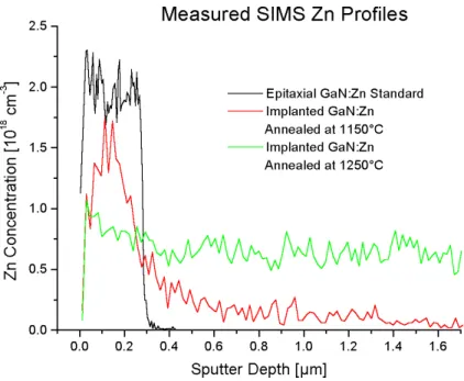
Figure 1 compares the Zn profiles measured by SIMS in the epitaxial GaN:Zn standard and the Zn-implanted samples annealed at 1150°C and 1250°C. The absolute Zn concentrations were estimated using the
reference value of 2 x 1018 cm-3 which was quoted by the Cree Research for the epitaxial GaN:Zn standard. The Zn profiles after the 1150°C and 1250°C anneals differ greatly, indicating that the onset of Zn diffusion occurs in this temperature range. The sample annealed at 1150°C shows a typical implantation profile consistent with what we measured earlier for 200 keV Zn+ in GaN [15] and the 1013 cm-2 Zn+ implantation dose. The 1250°C data do not resemble an ion implantation profile at all. SIMS observed the incorporation of significant Al and O with increasing annealing temperature, as well as detectable amounts of Na, K and Ca. The increased Zn background signal evident in the 1250°C profile is attributed to interference from the various impurities incorporated during the anneal. The annealing chamber had previously been used for a wide variety of experiments and material systems.
3.2. Photoluminescence
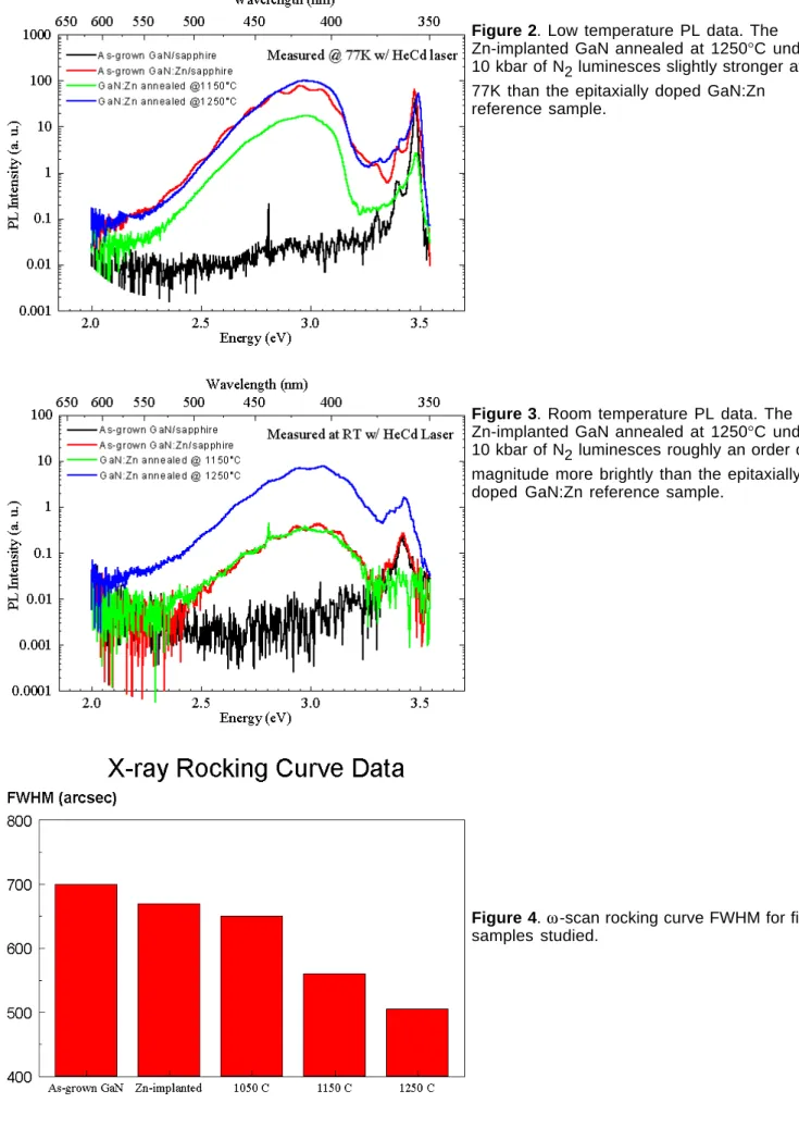
Figure 2 compares the 77K PL signals of the Zn-implanted samples annealed at 1150°C and 1250°C with the epitaxially doped GaN:Zn reference sample and the undoped GaN/sapphire starting material. The spectra are quite similar, differing only in magnitude, which confirms that high pressure annealing activated the implanted Zn acceptors. The sample annealed at 1250°C had slightly more intense Zn-related luminescence than the epitaxial GaN:Zn reference sample. The blue PL from the sample annealed at 1150°C was roughly an order of magnitude less intense.
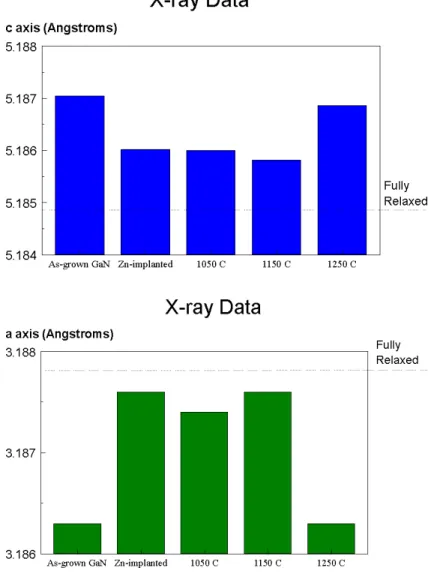
At room temperature (Figure 3), the Zn-related PL in the implanted samples was quenched less than the epitaxial GaN:Zn standard resulting in the 1250°C annealed sample luminescing roughly an order of magnitude more intensely than the reference sample in the blue. The 1150°C sample had a Zn-related PL intensity which was comparable to the epitaxially doped GaN:Zn reference sample.
3.3. High Resolution X-ray Diffractometry
X-ray rocking curves are generally a good measure of ion implantation damage and its removal via annealing, but it can be difficult to distinguish the broadening effects of strain and implantation damage using rocking curves alone. We therefore measured the GaN lattice parameters to independently monitor the residual strain in the heteroepitaxial films.
3.3.1. X-ray Rocking Curves
Figure 4 plots the measured rocking curve full width half maxima (FWHM) for unimplanted GaN/sapphire start material, and various Zn-implanted samples. The broadest rocking curve is obtained in as-grown
GaN/sapphire, even larger than the implanted, unannealed sample. Since there is no implantation damage in Downloaded from https:/www.cambridge.org/core. University of Basel Library, on 11 Jul 2017 at 15:48:59, subject to the Cambridge Core terms of use, available at https:/www.cambridge.org/core/terms.
pp , g p , p p g the as-grown material, the larger rocking curve FWHM must be attributed to residual strain in the film. The strain reduction achieved by the Zn implantation outweighs the influence of the implantation damage on the rocking curve width. Annealing at increasing temperatures continuously reduced the FWHM of the implanted samples. The narrower rocking curves correlate well with the PL intensities (Figure 2 and Figure 3) which increase with annealing temperature. The narrower rocking curves probably result from better crystal quality due to the annealing out of implantation damage and disorder.
3.3.2. Triple Axis X-ray Measurement of the Lattice Constants of Annealed GaN/sapphire Films
Figure 5a and Figure 5b plot the measured c-axis (perpendicular to the substrate plane) and a-axis (in-plane) lattice constants of the heteroepitaxial GaN, respectively. Also shown are estimates of the lattice constants which would be measured in unstrained GaN. GaN deposited on sapphire measured at room temperature is always observed to be under compressive strain due to the larger thermal expansion coefficient of sapphire and the post-growth cool down from the ~1100°C MOVPE growth temperature. The strain deduced to exist in the as-grown GaN/sapphire layer from the rocking curve FWHM is indeed apparent. We estimate that the observed strain in the unimplanted GaN/sapphire is 50±20% of that which would be expected purely from the thermal mismatch between GaN and the substrate. The considerable uncertainty in the quantification of the strain arises from the as yet unknown Poisson ratio for GaN among other factors. However, it is clear that the heteroepitaxial GaN film finds other mechanisms, probably involving the generation of structural defects, to relieve the thermal strain. Annealing at 1050°C or 1150°C does not affect the strain noticeably, while annealing at 1250°C increases the strain to a level comparable to the initial GaN/sapphire material.
4. Discussion
Both the SIMS and the x-ray observations suggest that the critical annealing temperature of Zn-implanted GaN lies between 1150°C and 1250°C. In this temperature range, the Zn becomes mobile in the GaN. The dopants can diffuse rapidly, and possibly even evaporate out of the film into the annealing chamber. Comparing the x-ray data of Figure 4 and Figure 5 taken on the 1150°C and 1250°C annealed GaN:Zn samples, the FWHM continues to decrease while the residual strain increases with the 1250°C treatment. We conclude that the increase in residual strain from the 1250°C to room temperature cool down is far outweighed by the structural improvement in the film realized by annealing at 1250°C. That the 1250°C annealed sample has a much narrower rocking curve width than the initial GaN/sapphire start material despite comparable amounts of strain, strongly suggests that annealing at 1250°C not only eliminates implantation damage, but other defects which previously existed in the heteroepitaxial start material.
Photoluminescence data at both 77K (Figure 2) and room temperature (Figure 3) indicate that annealing at 1250°C also activates the ion-implanted Zn acceptors in GaN. The Zn-related PL in the 1250°C sample was roughly an order of magnitude stronger than in the 1150°C sample at both temperatures. This is also strong evidence that the critical annealing temperature for structural repair of implanted GaN lies in the 1150°C - 1250°C temperature range.
The Zn PL signal in the 1250°C annealed sample exceeded that of the epitaxially grown GaN:Zn standard at both 77K and room temperature despite having an overall lower Zn concentration (Figure 1) and the various impurities introduced by the annealing process. This observation is consistent with the x-ray data in
suggesting that annealing of GaN at 1250°C under sufficient N2 overpressure removes more than simply the implantation damage.
While our study was carried out using Zn acceptors, high pressure annealing is promising for other acceptors. Electrical activation of Mg by high N2 overpressure annealing at higher temperatures (although below those causing diffusion) than presently used could yield a higher activation rate resulting from more efficient H removal. Even if such material is no better than p-type GaN:Mg activated by conventional atmospheric pressure annealing [17] [18], the high annealing temperatures attainable with kilobar N2 overpressure are not covered by existing patents [19] [20] which would promote wider commercialization of GaN device technology without onerous intellectual property constraints.
One difficulty with high temperature annealing under N2 overpressure for implanted dopant activation in GaN is the large amount of Zn diffusion which was observed at 1250°C. It is possible that equivalent improvement in the GaN material properties with much less diffusion could be realized by shortened annealing times.
High pressure annealing of GaN also raises the possibility of introducing dopants by diffusion. Promising acceptors such as Ca and Be are incompatible with MOVPE technology, but could be introduced by annealing
a GaN sample under kbar N2 overpressure in a chamber containing one or both of these elements. P-type contacts could also be improved if diffusion by high pressure annealing permits higher acceptor (e.g. Mg) concentrations to be introduced in the surface GaN.
5. Lateral GaN p-n Junction LED
The original goal of our ion-implantation study of GaN was to fabricate a monolithic, mulitcolor LED display, much like the one demonstrated in SiC [2], but with much better efficiency and color quality. Dmitriev et al. [2] achieved multicolor LED operation in SiC using masking to implant a regular pattern of three impurities which luminesce at different wavelengths into SiC, and later activating the dopants by thermal annealing.
We believe that the high temperature/pressure annealing approach for implanted dopant activation in GaN may enable an efficient lateral GaN LED to be fabricated solely by ion implantation. Figure 6 is a schematic of the proposed lateral LED device [21]. The lateral GaN LED could be fabricated in a typical GaN/sapphire heteroepitaxial layer. The n-type GaN top layer could be either epitaxially doped, or implanted with a donor such as Si. The active layer impurity is chosen based on the desired color, e.g. Zn for blue emission. The presence of Si in the active zone (if the top GaN layer is epitaxially doped) should not degrade or significantly shift the impurity emission since first generation Nichia LEDs were actually enhanced by Si co-doped active regions [22]. During operation, the Schottky contact is positively biased with respect to the ohmic contacts which causes electrons to be injected from the n-type GaN into the active zone where they recombine with the implanted acceptors.
6. Conclusion
We have annealed GaN at higher temperatures than previously possible by stabilizing the process under 10 kbar N2 overpressure. High temperature annealing under pressure has permitted the efficient optical
activation of ion-implanted impurities in GaN for the first time. Zn-implanted GaN annealed at 1250°C for 1 hr under 10 kbar of N2 overpressure exhibited stronger Zn photoluminescence than an epitaxially doped GaN:Zn reference sample at both 77K and room temperature. It is possible that yet higher PL efficiency from ion implanted Zn in GaN may be achievable at higher annealing temperatures, although the structural benefits of higher annealing temperature may be offset by increased impurity diffusion and evaporation of the impurity from the sample. At 10 kbar of N2 overpressure, it should be possible to anneal GaN samples at 1500°C without decomposition [4]. These experiments are underway and will be reported in a later publication.
Acknowledgments
We thank P. Baumgartner and Prof. A. Dommann of NTB Buchs for performing the Zn ion-implantation.
References
[1] S. Strite, H. Morkoç, J. Vac. Sci. Technol. B 10, 1237-1266 (1992).
[2] V. A. Dmitriev, Ya. V. Morozenko, I. V. Popov, A. V. Suvorov, A. L. Syrkin, V. E. Chelnokov, Sov. Tech. Phys. Lett. 12, 221 (1986).
[3] S. Strite, Monolithic Array of LEDs for the Generation of Light at Multiple Wavelengths and its use for Multicolor Display Applications, World Intellectual Property Organization Patent Number 11498 (1996) . [4] J. Karpinski, J. Jun, S. Porowski, J. Cryst. Growth 66, 1 (1984).
[5] J. I. Pankove, J. A. Hutchby, J. Appl. Phys. 47, 5387 (1976).
[6] J. I. Pankove, J. A. Hutchby, Appl. Phys. Lett. 24, 281 (1974).
[7] R. D. Metcalfe, D. Wickenden, W. C. Clark, J.Lumin. 16, 405 (1978).
[8] S. J. Pearton, C. B. Vartuli , J. C. Zolper , C. Yuan, R. A. Stall , Appl. Phys. Lett. 67, 1435-1437 (1995).
[ ] , , p , , , pp y , ( )
[9] J. W. Lee, S. J. Pearton , J. C. Zolper , R. A. Stall , Appl. Phys. Lett. 68, 2102-2104 (1996).
[10] R. G. Wilson , S. J. Pearton, C. R. Abernathy , J. M. Zavada , Appl. Phys. Lett. 66, 2238-2240 (1995).
[11] J. C. Zolper, M. Hagerott-Crawford, S. J. Pearton, C. R. Abernathy, C. B. Vartuli, C. Yuan, R. A. Stall, J. Electron. Mater. 25, 839-844 (1996).
[12] R. G. Wilson, C. B. Vartuli, C. R. Abernathy, S. J. Pearton, J. M. Zavada, Sol. St. Electr. 38, 1329-1333 (1995).
[13] S. C. Binari, H. B. Dietrich, G. Kelner, L. B. Rowland, K. Doverspike , D. K. Wickenden , J. Appl. Phys. 78, 3008-3011 (1995).
[14] J. C. Zolper , R. G. Wilson , S. J. Pearton , R. A. Stall , Appl. Phys. Lett. 68, 1945-1947 (1996).
[15] S. Strite, P. W. Epperlein, A. Dommann, A. Rockett, R. F. Broom, Mater. Res. Soc. Symp. Proc. 395, 795-800 (1996).
[16] A. Pelzmann, S. Strite, A. Dommann, C. Kirchner, Markus Kamp , K. J. Ebeling, A. Nazzal, MRS Internet J. Nitride Semicond. Res. 2, 4 (1997).
[17] H. Amano, M. Kito, K. Hiramatsu, I. Akasaki, Jpn. J. Appl. Phys. 28, L2112 (1989).
[18] S. Nakamura, T. Mukai, M. Senoh, N. Iwasa, Jpn. J. Appl. Phys. 31, L139-L142 (1992).
[19] H. Amano, I Akasaki, T. Tanaka, T. Tohma, K. Manabe, Method for producing a luminous element of III-group nitride, United States Patent Office Patent Number 5496766 (1996) .
[20] S. Nakamura, S. Iwasa, M. Senoh, Method of manufacturing p-type compound semiconductor, United States Patent Office Patent Number 5306662 (1994) .
[21] R. L. Melcher, S. Strite, IBM Tech. Disc. Bull. 39, 75 (1996).
[22] Shuji Nakamura , J. Vac. Sci. Technol. A 13, 705-710 (1995).
Figure 1. SIMS Zn profiles measured on the epitaxially grown GaN:Zn standard, and implanted samples annealed at 1150°C and 1250°C for 1 hour under 10 kbar of N2 overpressure.
Figure 2. Low temperature PL data. The Zn-implanted GaN annealed at 1250°C under 10 kbar of N2 luminesces slightly stronger at 77K than the epitaxially doped GaN:Zn reference sample.
Figure 3. Room temperature PL data. The Zn-implanted GaN annealed at 1250°C under 10 kbar of N2 luminesces roughly an order of magnitude more brightly than the epitaxially doped GaN:Zn reference sample.
Figure 4. ω-scan rocking curve FWHM for five samples studied.
Figure 5a. c-axis lattice constants from triple axis x-ray measurements.
Figure 5b. a-axis lattice constants from triple axis x-ray measurements.
Figure 6. Proposed lateral GaN LED structure whose color depends on the impurity
implanted in the active zone.
© 1997 The Materials Research Society