HAL Id: tel-02441820
https://tel.archives-ouvertes.fr/tel-02441820
Submitted on 16 Jan 2020HAL is a multi-disciplinary open access
archive for the deposit and dissemination of sci-entific research documents, whether they are pub-lished or not. The documents may come from teaching and research institutions in France or abroad, or from public or private research centers.
L’archive ouverte pluridisciplinaire HAL, est destinée au dépôt et à la diffusion de documents scientifiques de niveau recherche, publiés ou non, émanant des établissements d’enseignement et de recherche français ou étrangers, des laboratoires publics ou privés.
Elaboration de films de perovskites hybrides par
coévaporation pour des applications photovoltaïques.
Chloe Dindault
To cite this version:
Chloe Dindault. Elaboration de films de perovskites hybrides par coévaporation pour des applications photovoltaïques.. Material chemistry. Université Paris Saclay (COmUE), 2019. English. �NNT : 2019SACLX079�. �tel-02441820�
Development of coevaporated
perovskite thin films
for tandem solar cells applications.
Thèse de doctorat de l'Université Paris-Saclay
préparée à l’Ecole Polytechnique
École doctorale n°573 Interfaces :
approches interdisciplinaires,
fondements, applications et innovation (Interfaces)
Spécialité de doctorat: Physique
Thèse présentée et soutenue à Palaiseau, le 8 octobre 2019, par
Chloé DINDAULT
Composition du Jury :
Mme Nadine Witkowski Présidente
Professeure, Sorbonne Université, Institut des NanoSciences de Paris (CNRS)
Mme Mireille Richard-Plouet Rapportrice
Directeure de Recherche, Université de Nantes, Institut des Matériaux Jean Rouxel (CNRS)
Mr Benoit Lessard Examinateur
Maître de Conférences, Université d’Ottawa
Mr Matthieu Manceau Examinateur
Ingénieur de Recherche, Institut National pour l’Energie Solaire (CEA-LITEN)
Mr Rachid Belkhou Examinateur
Chercheur, Responsable de ligne de lumière, Synchrotron SOLEIL (CNRS/CEA), Université Paris-Saclay
Mr Yvan Bonnassieux Directeur de thèse
Professeur, Ecole Polytechnique, Laboratoire de Physique des Interfaces et des Couches Minces (Ecole Polytechnique/CNRS), IP Paris
Mr Denis Tondelier Co-Directeur de thèse
Ingénieur de recherche, Laboratoire de Physique des Interfaces et des Couches Minces (Ecole Polytechnique/CNRS), IP Paris
NNT
:
2
0
1
9
S
A
CL
X
0
7
9
i
Acknowledgments
For this part, I will switch to French.
Je voudrais tout d’abord naturellement remercier mon encadrement : Yvan, Denis et Bernard (même si tu n’apparais pas officiellement tu as toujours été là, pas loin, et toujours pertinent). Vous avez cru en moi dès le début, dès mon stage de M2 en février 2016 et vous vous êtes battus pour me garder. Vous avez appris à travailler avec moi et mon (fort) caractère. Cela n’a pas toujours été facile mais vous avez su être là dans les moments clefs. Je vous remercie sincèrement de la confiance que vous m’avez faite très tôt et de l’indépendance que vous m’avez offerte, essentielle pour moi.
Tout naturellement je passe ensuite à ceux sans qui ce travail n’aurait pas pu être mené : l’IPVF avec particulièrement Bruno Carlotti puis Roch Drozdowski-Strehl et Christophe Bonelli et le LPICM avec Pere Roca i Cabarrocas. Vous m’avez offert un environnement de travail dans lequel j’ai pu m’épanouir pleinement. Dans la continuité, je tiens à remercier les équipes supports de l’IPVF avec notamment Sonia Haouka, Bérengère Larue, Ariana Salemi puis Viviane Bastiao. Même si je ne passais dans les locaux de l’IPVF qu’une fois par mois pour récupérer mon bulletin de salaire, vous m’avez toujours tous accueillie avec le sourire. Je tiens ensuite à remercier tout particulièrement Alexis Denis pour son aide pendant le déménagement de l’équipement du LPICM vers l’IPVF puis pendant la phase de remise en service. Je remercie aussi l’équipe du projet F, porté par Jean Rousset, notamment Amelle Rebai, Javier Ramos et Florian Hilt avec qui j’ai le plus interagi mais aussi tous les autres. Enfin, je remercie tous les chercheurs IPVF, nos effectifs ont bien grandi depuis mon arrivée dans la structure, continuez les efforts menés afin de réaliser les objectifs que l’IPVF s’est fixé.
Je souhaite ensuite adresser de sincères remerciements à la totalité du laboratoire LPICM dans lequel j’ai passé le plus clair de mes journées ces trois dernières années. Je pense particulièrement à Gabie, Jérôme, Eric, Marc, Guillaume, Rafaël, Mengkoing, Alaric, Nicolas, Tiphaine, Ghewa et Romain avec qui j’ai passé d’agréables moments autour d’un café, d’une raclette ou de bières. Merci à l’ensemble de l’équipe OLAE (Organic Large Area Electronics) et plus particulièrement à notre équipe réduite perovskites et ces différents membres : Warda, Heejae, Arthur, Alexandre, Eric, Jonas, Tiphaine, Hindia, Minjin, Corentin, Khaoula et Hae-Yeon (doctorants, post-doctorants et stagiaires par ordre chronologique) ainsi que Yvan, Bernard, Denis et Jean-Eric pour les discussions et échanges, toujours riches.
Je tiens maintenant à remercier les différents collaborateurs rencontrés dans le cadre de notre étude en Synchrotron. Maxime, c’est avec toi que tout a commencé entre le LPICM et la ligne de lumière HERMES à SOLEIL. Je me rappellerai longtemps de quelques nuits à travailler jusqu’à 2h du matin, à supporter ton humour (de 2h du matin lui aussi…) et croiser les doigts que le faisceau ne coupe pas. Sufal, grâce à toi j’ai pu prendre les rênes de cette collaboration sereinement à la suite de Maxime. Tu as été d’une grande aide au travers des différentes campagnes de mesures mais encore plus en dehors de celles-ci, lors du traitement des données. Philip ton arrivée ne pouvait pas mieux tomber, ton expertise et ton énergie ont su donner un nouvel élan à notre petite équipe STXM/Perovskites. C’est un réel plaisir (et une certaine fierté) de voir que les choses se pérennisent et qu’une thèse en collaboration entre le LPICM et HERMES est sur le point de commencer.
ii
Je passe maintenant aux remerciements plus personnels. Ce manuscrit n’existerait sûrement pas sans le soutien sans faille des quelques personnes suivantes : Fabienne, Marlinka, Hindia, Anna, Tanguy, Ronan, Patxi et Cyril. Vous m’avez tous supportée pendant ces longs mois de rédaction (et bien avant aussi, mais j’étais encore relativement supportable à l’époque).
Fabienne, je crois que mon épanouissement personnel dans ce laboratoire a commencé avec toi. J’ai très vite été épanouie professionnellement dans ce cadre de travail mais il m’a fallu du temps pour sortir de ma bulle, enlever ces écouteurs constamment vissés sur mes oreilles, prendre le temps de faire des pauses dans mon travail et prendre du recul. Tout ça est venu avec toi, avec ton amitié, avec ta folie et avec ton énergie. Tu rayonnes tout simplement. J’ai trouvé en toi une amie avec qui parler, chanter, danser, pleurer mais surtout rire et sourire. On a du mal à se rappeler le moment exact depuis lequel on se parle, je crois que c’est parce que j’ai l’impression de t’avoir toujours eu à mes côtés dans cette folle aventure. Tu n’as pas idée de ce que je te dois, je n’aurai pas pu réaliser la moitié de ce que j’ai fait sans toi. Cette thèse existe grâce à ton amitié et ton soutien. Je suis heureuse de t’avoir à mes côtés dans la vie, pour de longues années.
Malinka, il aura fallu que le préfabriqué 404 de l’équipe Total ferme pour que tu migres vers nos locaux et que notre amitié commence. Depuis, on a rattrapé le temps perdu je crois. J’ai très vite trouvé en toi bien plus qu’une simple camarade de repas et de virées à la boulangerie ou à la piscine, j’ai trouvé en toi une véritable amie. Tu as été d’une aide précieuse ces derniers mois, bien plus que je ne saurai le retranscrire ici. C’est à ton tour maintenant de te lancer dans la rédaction. Vas-y, tu verras c’est super ! … Tu as tout ce qu’il faut pour le faire. Je "t’abandonne" au pire moment. Je ne pourrai malheureusement pas être là (physiquement) pour te soutenir, t’accompagner dans cette aventure mais tu sais que tu peux compter sur moi, comme j’ai pu compter sur toi, pour t’écrire des messages de motivation, te remonter le moral quand ça n’ira pas, te gronder quand tu baisseras les bras, te féliciter quand tu auras fini des chapitres, t’aider à relativiser (la ‘sagesse’ de ceux qui y sont passés), te rappeler que même si c’est dur tu vas y arriver. Mais je serai là aussi (et surtout !) pour parler de tout sauf de la thèse. À tout moment, n’hésite pas. On se donne rendez-vous à Lyon, pour partager des restau, des spectacles et des apéros, à nos années d’amitié à venir !
Hindia, Anna et Tanguy je vous regroupe car vous avez été mes co-bureaux pendant cette thèse mais vous êtes devenus bien plus que cela… de vrais et chers amis. Vous avez été les plus exposés à mon humeur (souvent mauvaise) lors de la rédaction de ce manuscrit, à mes inquiétudes, à mes sautes d’humeur, à mes larmes de joie et de stress, à mes capacités vocales (mauvaises), à mes moyens (débiles) de décompresser (faire des bulles, me coller des gobelets sur le front ou essayer d’éteindre la lumière du bureau en tirant sur l’interrupteur avec un pistolet NERF…) et à mes périodes d’euphorie à la fin d’un chapitre et de doutes au début du suivant. Pour certains, notre bureau est le plus bruyant du bâtiment, pour moi c’est… effectivement le plus bruyant mais c’est aussi un bureau rempli de bonnes ondes, de mots (plus ou moins scientifiques) écrits au tableau, de bonbons, de madeleines, de compotes et de plantes (dédicace Bob et RIP ton orchidée trop tôt lâchement assassinée Tanguy…). Bref, le meilleur bureau (même si j’ai toujours eu la pire des chaises et le plus petit des bureaux…). Prenez en soin !
iii
Ronan, il t’aura suffi de 2h pour me donner le déclic après 2 semaines à être bloquée sur ce chapitre 3. La sagesse du post-doc sûrement… Avec toi et Malinka on a formé un sacré trio, à se retrouver bien souvent après 18h30 dans la cafétéria pour débriefer de la journée ou de nos week-ends/vacances, autour d’un encas (voire d’un repas complet pour toi…). Merci pour ta patience, ton soutien et ton amitié.
Patxi, ton insupportable bonne humeur aura plus d’une fois eue raison de mon humeur grincheuse. Je ne vais pas dire que c’est un succès total mais je crois qu’à force d’acharnement tu as un peu réussi à me faire relativiser les choses. Merci pour tes encouragements chaque fois que tu passais devant le bureau ces derniers mois. Tu as été un soutien indéfectible, parfois dur dans tes mots (quand il le fallait) tu as toujours été juste et honnête à mon égard. Ton soutien a été d’une importance cruciale, plus que tu ne peux le réaliser. Enfin, je tiens à t’adresser un merci tout sauf anecdotique d’avoir rendu réel un objet que j’ai pensé dès mon arrivée au laboratoire.
Cyril, tu as toujours pris le temps de dépanner mes différents équipements tout en m’expliquant chaque fois (quitte à parfois te répéter) les opérations menées. Grâce à toi j’ai étendu mon lexique avec des mots comme ‘tombac, Fomblin, colliers, jauge, vanne, etc…’. Mais tu ne t’es pas arrêté au seul soutien technique, tu as aussi (souvent) pris le temps de me remonter le moral et de m’aider à voir les choses différemment. Tu diras certainement que l’accompagnement des doctorants fait partie de ton travail (et c’est là toute la modestie qui te caractérise), mais j’aime à penser que tu l’as fait parce tu as sincèrement cru en moi, dès le début, pas seulement parce que tu es professionnellement consciencieux. Merci pour ton soutien et ta patience mais aussi (et surtout) ta gentillesse.
Je conclurai en remerciant ma famille : mes parents Sylvaine et François, ma sœur Estelle, mon frère Cédric, ma tante Marie-Luce, mon beau-frère Geoffrey, mon neveu Léandre et toi petit bébé qui n’est pas encore là mais qui fait déjà de moi une tante doublement heureuse, et mes amis : Elodie, Adeline, Clémence, Ophélie, Sébastien et Valentin. Merci à chacun d’entre vous pour votre amour inconditionnel. Dans les moments difficiles je n’ai pas lâché, me disant que cette thèse si je ne la faisais pas pour moi, au moins je la faisais pour vous, pour vous rendre fiers. Je ne vais pas plus m’épancher ici, sachez juste que tant que vous êtes tous à mes côtés, je sais que je suis sur le bon chemin.
v
List of abbreviations
2/3/4T: 2/3/4-terminal a-Si: amorphous Silicon ALS: Advanced Light Source APS: Advanced Photon Source
ARPES: Angle-Resolved PhotoEmission Spectroscopy BCP: 1-(1,3-Benzodioxol-5-ylCarbonyl) Piperidine c-Si: crystalline Silicon
CB: ChloroBenzene
CIGS: Copper Indium Gallium Selenide CLS: Canadian Light Source
DMF: N,N-DiMethylFormamide DMSO: DiMethylSulfOxide DSSC: Dye-Sensitized Solar Cell
EELS: Electron Energy Loss Spectroscopy ESRF: European Synchrotron Facility ETL: Electron Transporting Layer
EXAFS: Extended X-ray Absorption Fine Structure FAI: Formamidinium Iodide
FET: Field-Effect Transistor FIB: Focused Ion Beam
FTIR: Fourier Transform InfraRed FZP: Fresnel Zone Plate
GI-WAXD: Grazing-Incidence Wide Angle X-ray Diffraction GI-WAXS: Grazing Incidence Wide Angle X-ray Scattering GI-XRD: Grazing Incidence X-ray Diffraction
HERMES: High Efficiency and Resolution beamline for X-ray Microscopy and Electron Spectroscopy
HTL: Hole Transporting Layer ICL: InterConnecting Layer ITO: Indium Tin Oxide LED: Light Emitting Diode LINAC: LINear ACcelerator MAI: MethylAmmonium Iodide
NEXAFS: Near-Edge X-ray Absorption Fine Structure NSLS: National Synchrotron Light Source
NSRRC: National Synchrotron Radiation Research Center OD: Optical Density
OLED: Organic Light Emitting Diode OSA: Order Sorting Aperture
PCBM: Phenyl-C61-Butyric acid Methyl ester
PEA(I): PhenylEthylAmmonium (Iodide)
PEDOT:PSS: Poly(3,4-EthyleneDioxyThiophene) PolyStyrene Sulfonate PF: Photon Factory
PLS: Pohang Light Source
vi PV: PhotoVoltaics
QCM: Quartz Crystal Microbalance SAT: Site Acceptance Tests
SEM: Scanning Electron Microscopy SLS: Synchrotron LightSource
SOLEIL: Source Optimisée de Lumière d'Energie Intermédiaire du LURE SPEM: Scanning PhotoEmission Microscopy
SR: Synchrotron Radiation
SRPES: Synchrotron Radiation PhotoEmission Spectroscopy SSRF: Shanghai Synchrotron Radiation Facility
SSRL: Stanford Synchrotron Radiation Lightsource STXM: Scanning Transmission X-ray Microscopy TEM: Transmission Electron Microscopy
TEY: Total Electron Yield
UVSOR: UltraViolet Synchrotron Orbital Radiation WAXS: Wide Angle X-ray Scattering
XANES: X-ray Absorption
XAS: X-ray Absorption Spectroscopy XPS: X-ray Photoelectron Spectroscopy XRD: X-Ray Diffraction
vii
Table of content
Acknowledgments i
List of abbreviations v
Emerging photovoltaics: the key to photovoltaics democratization? 1
Thesis aim and outline 3
Chapter 1. 5
A glimpse of hybrid perovskites for photovoltaic applications: 5
focus on the deposition methods. 5
Introduction 7
I. Perovskites 8
II. Photovoltaic effect and solar cells 10
III. Perovskites in PV 13
i. New perovskite compositions 15
ii. New types of cells 16
iii. New manufacturing processes 18
IV. ‘Simple’ CH3NH3PbI3 thin films fabrication by coevaporation 22
Conclusion 27
Chapter 2. 29
Design and engineering of a reactor for perovskite coevaporation. 29
Introduction 31
I. Coevaporation process for perovskites using a proof-of-concept reactor 32 i. Initial developments and identification of missing features 32
ii. Proof-of-concept assessment results 37
II. Comparison of the specifically designed reactor with the proof-of-concept one 41 III. Implementation of the new reactor designed for perovskite coevaporation 43
i. Site Acceptance Tests 43
ii. Transfer knowledge between equipments 46
iii. Single compound depositions 49
iv. Toward coevaporation 53
viii
Chapter 3. 57
Fabrication of perovskite thin films using coevaporation. 57
Introduction 59
I. Coevaporation process for perovskite thin films 60
i. Focus on the process repeatability 60
ii. Focus on the material properties 67
II. Open discussions 76
i. Process-related aspects 76
ii. Material-related aspects 76
Conclusion 78
Chapter 4. 79
Nanoscale characterisation of perovskite films using Synchrotron-based technique. 79
Introduction 81
I. X-ray radiation 82
II. X-ray Absorption Spectroscopy 83
III. Synchrotron lightsource 85
i. Synchrotron radiation 85
ii. Synchrotron facility 86
IV. Scanning Transmission X-ray Microscopy 88
i. History and development 88
ii. STXM instrumentation 91
iii. STXM measurements 92
V. Synchrotron-based studies of perovskite films 95
VI. LPICM perovskite team STXM studies 96
VII. Homogeneity of wet- and dry-perovskite films assessed by Synchrotron STXM 98
i. Samples preparation 98
ii. STXM Measurements 100
iii. Post-processing methodology 105
iv. Ratio calculations results 109
v. Open discussion 113
ix
Conclusion and Perspectives 115
List of references a
Annexes B
Fabrication of perovskite solar cells at LPICM A
1
Emerging photovoltaics: the key to photovoltaics
democratization?
In the current climate crisis context, more and more citizens are looking for ways to contribute to the fight against global warming at their own humble level. People are trying to limit their negative impact on the planet: decreasing their meat consumption, avoiding plastics, limiting their carbon footprint, recycling, embracing a zero waste philosophy lifestyle. In the present digital era, rethinking our electricity consumption appears equally relevant. Indeed, electricity is becoming “the fuel of choice” accounting for 20% of the global final consumption according to IEA’s 2018 World Energy Outlook report 1.
Based on abundant, sustainable and available resources, solar photovoltaic (PV) and wind power stand as the most obvious choices, among renewables, to generate green electricity. Although well adapted for large scale facilities, wind power cannot be easily implemented at the local level by climate-concerned citizens. Indeed, wind turbines are rarely installed in the backyard of a suburban house while, on the other hand, solar panels are widely deployed on their rooftops. Solar PV then stands as the most convenient technology for small-scale green electricity production.
Although the photovoltaic market is dominated by Silicon, historical actor of the field and the current most efficient technology, there is indubitably room for parallel niche markets where the so called emerging technologies, such as organic and perovskite PV, would perfectly fit. In the optics of democratizing photovoltaics, chosen technologies should be cheap, easy to implement and adaptive. Manufactured from low cost materials, using low cost processes, organic and perovskite PV are cheaper than Silicon. Based on thinner absorbing layers, they offer a flexibility and a lightness that Silicon fails to provide. In addition, their colourfulness brings an aesthetical feature into the matter that would further broaden the range of possibilities.
Being older than its perovskite counterpart, organic PV can already claim (despite its relatively low efficiencies) several successful implementations and realisations among which: OPVIUS’s solar trees implemented at the entrance of Merck headquarters in Germany2,
Heliatek’s flexible organic solar films installed on canopies at the Roland Garros French Open3 and ARMOR’s OPV film ‘ASCA’ installed on horticultural greenhouses4.
Possessing all the features that make OPV appealing while reaching higher efficiencies, perovskites seem to be the perfect material for market penetration. Despite their youthfulness in the photovoltaic field, perovskites transfer from the laboratory to the industry is already initiated with companies such as Saule Technologies and Oxford PV.
In November 2016, Oxford PV took a huge step toward commercialization of perovskite solar cells, securing the acquisition of a former Bosch Solar CISTech GmbH production site5, equipped with 17,000 m² of pilot line facilities. In July 2019, ‘The perovskite
1 Internation Energy Agency 2018 World Energy Outlook report 2 Merckgroup.com
3 Heliatek.com 4 Asca.com
2 company’ secured a £65 million funding6 to push further the development of their
vacuum-processed perovskite based tandem approach. At the end of 2018, the Polish start up Saule Technologies announced the installation of their inkjet-printed perovskite solar modules at Henn-na hotel in Japan7. Few months later, they were launching a pilot installation on
Skanska’s offices in Warsaw8. Although no products are yet available, both Saule
technologies and Oxford PV are unquestionable driving forces in the race of perovskite PV toward the market.
6 OxfordPV.com / news 3rd July 2019 7 Sauletech.com
3
Thesis aim and outline
This thesis was carried out in the framework of the Project F “Perovskite solar cells” of the Institut Photovoltaïque d’Île-de-France (IPVF) in close collaboration with the Laboratoire de Physique des Interfaces et des Couches Minces (LPICM) from CNRS (UMR 7647) and Ecole Polytechnique. IPVF’s project F addresses three major aspects of the perovskite photovoltaics field: device stability, large surface deposition and tandem applications.
The present thesis covers the last two topics of IPVF project F as the objective is to develop, using a semi-industrial reactor, the coevaporation process for perovskite thin films fabrication with the target of tandem applications.
The first chapter of the manuscript will introduce the reader to the perovskite materials, their characteristics and properties to eventually direct the interest toward their use as light absorber in solar cells. Navigating through the progress made in the field of perovskite photovoltaics we will ultimately focus on the processing methods. Following an overview of the different methods for perovskite thin films fabrication, we will narrow down the scope to the coevaporation process. Finally, discussing a literature review of the topic will provide some basic insights on the method used in the follow-up chapters.
The second part of the manuscript will take the reader through the early stages of our development of the coevaporation process for perovskite thin films fabrication. Starting off on a proof-of-concept reactor, our initial developments will drive us to design a second reactor, dedicated to perovskite coevaporation. The implementation and initial trials on this new reactor will be detailed, setting the ground for the next chapter.
The third part of the manuscript will be dedicated to the development of the coevaporation process using the specifically designed reactor. In the hope of taming the deposition technique the focus will be first given to process-related considerations. Eventually properties of the fabricated materials will be studied, discussed and correlated to the deposition conditions. From these results, various aspects will be debated, paving the way for future developments.
The last part of the manuscript will take the reader to new horizons, away from the perovskite thin films fabrication toward their characterization using a Synchrotron-based technique. After a thorough introduction to the lightsource world, we will eventually introduce the X-ray based spectromicroscopy technique used to study our perovskite films. Results of our study will then be disclosed and discussed.
Ultimately, general conclusions from the previous four parts will be drawn and ideas for future research will be provided.
5
Chapter 1.
A glimpse of hybrid perovskites for
photovoltaic applications:
focus on the deposition methods.
Michael Saliba: - “New world record for perovskite solar cells at 25.2% KRICT/MIT. […]” Aron Huckaba: - “Wow! Can’t wait to see how they did it.”
Michael Saliba: - “Will be very exciting. Although not even the previous record is published yet haha” Twitter @miliba01, August 3rd 2019
7
Introduction
The present chapter aims at setting the scene for the rest of the manuscript. Following a brief synopsis on the perovskite family and their outstanding optoelectronic properties, we will address key concepts of photovoltaics through its history, theory and applications, these latter being our interest in the framework of this thesis.
We will eventually resume to the history of perovskites in the photovoltaic field. The first use of perovskites as light absorber goes back to only a decade ago. It then quickly became a trending topic, such that perovskites are now directly challenging the historical actors of the field. Along the way, tremendous progresses were achieved on the levels of: composition, cell types and deposition processes. We will provide insights on each of these topics with a particular focus on these latter.
Achieving high efficiencies at low cost, perovskites have all it takes for a great industrial future. We will eventually direct our interest towards the coevaporation process for perovskite solar cells. This vacuum-based technique, already widely implemented in the OLED industry for example, stands as a viable candidate for the manufacturing of large area perovskite thin films.
8
I.
Perovskites
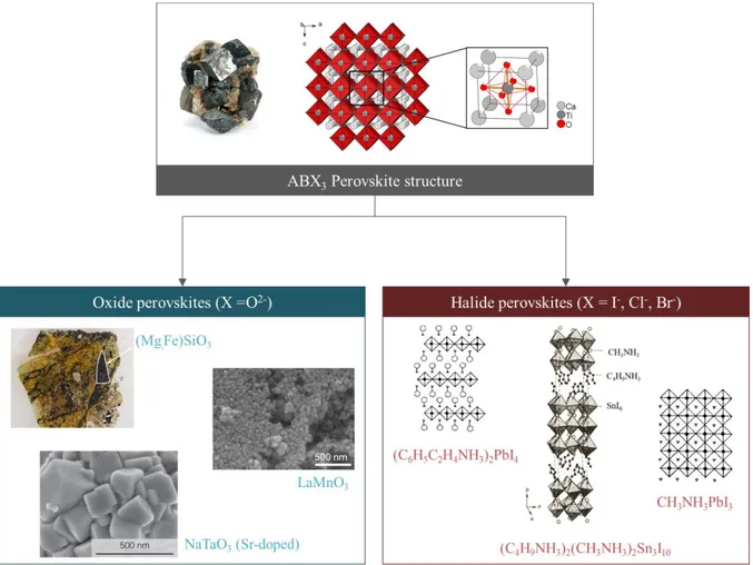
In 1839, German mineralogist Gustav Rose discovered a calcium titanate mineral of chemical formula CaTiO3. The crystal structure consists of a TiO6 octahedron inside a
Ca8 cube, in 3D it can be seen as a network of corner-sharing octahedra with Calcium-filled
cavities (Figure 1). The arrangement can be reduced to its unit cell formula ABX3, A being
the corner atoms in the cubic lattice, B the centre atom and X the face centred ones. As a tribute to the Russian mineralogist Lev Alexeïevitch Perovski the structure was named ‘perovskite’. Depending on the nature of the X-site atom, subfamilies can be defined: oxide (X = O2-)9,10,11,12,13 and halide (X = I-, Cl- or Br-) perovskites.
Figure 1. Perovskite family tree: from the parent general ABX3 crystal structure14 (with CaTiO3 mineral15) to the
oxide subfamily with (Mg,Fe)SiO3 bridgmanite from Earth lower mantle16, catalytic LaMnO313 and Sr-doped
NaTaO317 and halide subfamily with (C6H5C2H4NH3)2PbI418, (C4H9NH3)2(CH3NH3)2Sn3I1019 and CH3NH3PbI318.
9 E. Knittle and R. Jeanloz, (1987) Science 235, 668 10 F. Nestola et al., (2018) Nature, 555, 237-41
11 M. F. M. Zwinkels et al., (1999) Catalysis Today, 47, 73-82 12 H. Huang et al., (2019) Diamond & Related Materials, 91, 199-206 13 Q. Wang and L. Ma, (2019) New J. Chem., 43, 2974-80
14 adapted from N. Louvain’s thesis manuscript « Relations Structures-Propriétés dans des matériaux hybrides multifonctionnels : Investigations structurales et théoriques. » (2008) <tel-00450691>
15 Wikipedia
16 Earth-Building Bridgmanite; Caltech (2014) 17 L. An and H. Onishi, (2015) ACS Catal., 5, 3196-206 18 T. Ishihara, (1994) J. of Luminescence, 60 & 61, 269-74 19 D. B. Mitzi et al., (1994) Nature, 369, 467-9
9 Considering halide perovskites, B-site is occupied by a dication like Pb2+, Sn2+20, Bi2+21
or Ge2+22 (either pure or mixed23,24) and A-site can be occupied by a large variety of univalent
cations (organic or not). If the A-cation is too big, the 3D network is shattered, leading to layered perovskites with a dimensionality of 2. By fine molecular engineering, intermediate 2 to 3D phases can even be obtained25. Although, strictly speaking ‘perovskite’ refers to the
3D arrangement, lower dimension materials also fall under the perovskite banner, as derived from the parent structure, making this family a rather complex and wide one.
Whatever their dimensionality, halide perovskites have quite outstanding properties of photoconductivity as reported in 1958 by Møller for Caesium halide perovskite CsPbX326 and
later on in 1978 by Weber for the hybrid organic-inorganic lead halide perovskites CH3NH3SnBrxI3-x27 and CH3NH3PbX328 (a non-exhaustive yet very complete review can be
found in Mitzi29). Therefore, halide perovskites can be integrated in a variety of optoelectronic
devices such as Light Emitting Diodes (LED)30, Field Effect Transistors (FET)31 or Solar
Cells32 (Figure 2). Throughout this document, focus is given to the solar cell applications.
Figure 2. Examples of halide perovskite-based optoelectronic devices: CH3NH3PbX3 Field-Effect Transistor31
(S, D and G being Source, Drain and Gate), CH3NH3PbI3 Solar cell33 and CH3NH3PbBr3 Light Emitting Diode34.
The love story between perovskites and photovoltaics is quite recent, being only ten years old. In 2009, Kojima et al.35 used CH
3NH3PbI3 in Dye-Sensitized Solar Cells (DSSC)
yielding 3.8% efficiency. Since then, perovskite photovoltaics has taken off as its own technology: new cells were developed and higher efficiencies have been achieved. Before going any deeper into this story, let us take a step aside to focus on photovoltaics: its history and theory.
20 F. Hao et al., (2014) Nat. Photon., 8, 489-94 21 B-W. Park et al., (2015) Adv. Mater., 27, 6806-13
22 G. Stoumpos et al., (2015) J. Am. Chem. Soc.,137, 21, 6804-19 23 S. Lee et al., (2018) 227, 311-4
24 N. Ito et al., (2018) J. Phys. Chem. Lett., 97, 1682-8
25 A. Leblanc et al., (2017) Angew. Chem. Int. Ed., 56, 16067-72 26 C. K. Møller, (1958) Nature, 182, 1436
27 D. Weber, (1978) Zeitschrift für Naturforschung B, 33, 8, 862-5 28 D. Weber, (1978) Zeitschrift für Naturforschung B, 33, 12, 1443-5
29 D. B. Mitzi ‘Synthesis, Structure, and Properties of Organic‐Inorganic Perovskites and Related Materials’ in Progress in Inorganic Chemistry, K. D. Karlin (1999)
30 Y. H. Kim et al., (2015) Adv. Mater., 27, 1248 31 W. Yu et al., (2018) Nature Communications, 9, 354 32 M. Grätzel, (2014) Nature Materials, 13, 838–42 33 O. Almora et al., Rev. Cub. Fís. (2017), 34, 1, 58-68 34 H. Cho et al., (2015) Science, 4, 350, 6265, 1222-5 35 A. Kojima et al., (2009) J. Am. Chem. Soc., 131, 17, 6050-1
10
II.
Photovoltaic effect and solar cells
Discovered in 1839 by the French physicist Alexandre Edmond Becquerel36, the
photovoltaic effect depicts the conversion of light into electricity by a material. Photovoltaic active materials are empirically sorted out in three generations: Silicon (poly- and mono-crystalline), thin films (CIGS, CdTe, amorphous Si) and the so-called “emerging PV” that gathers organic and quantum dots among other technologies. If each generation has its own specificities, solar cells all basically operate in the same way.
At the heart of the solar cell is the semi-conductor absorbing layer (Figure 3). Semi-conductor materials are defined by a non-zero conduction-to-valence bandgap (Eg), typically of a few eV (above tens of eV the material can be considered as insulating). Their illumination promotes one conduction band electron to the valence band, creating an electron/hole pair in the absorber. Due to the energy difference between the carrier-selective layers, generated charges are separated and finally collected at the electrodes. The overall process creates an electrical current in the device and its efficiency is estimated by the produced to incident power ratio, i. e. the electricity to light ratio.
Figure 3. Photoconversion process steps: 1. Photon (hν) absorption; 2. electron/hole (e-/h+) pair creation; 3.
charges separation; 4. charges collection and 5. current generation (VB and CB: Valence and Conduction Bands and Eg the bandgap).
Experimentally, solar cells are characterized by current-voltage measurements: a voltage bias (V) is applied to a device under illumination and the current (I) delivered is measured. From the obtained J-V curve (very often, the current density J is preferred to the current I), one can extract three important values: the open circuit voltage (Voc), the
short-circuit current density (Jsc) and the Fill Factor (FF) and calculate a fourth one: the
photoconversion efficiency (PCE). This set of parameters defines the device. As depicted on the J-V curve in Figure 4, Voc and Jsc are defined as the voltage value for a zero current
density and the current density value for a zero voltage respectively. The Fill Factor is calculated as the ratio of the maximal power (mp) actually delivered by the cell over the power if the cell was ideal (equation [1]). It depicts the device ideality gap, i. e. the closer it gets to 1, the more optimized the device is. Finally, the PCE is calculated as the ratio of the produced power over the incident power (equation [2]).
11 𝐹𝐹 =𝑉𝑚𝑝× 𝐽𝑚𝑝 𝑉𝑜𝑐× 𝐽𝑠𝑐 [1] 𝑃𝐶𝐸 =𝑃𝑝𝑟𝑜𝑑 𝑃𝑖𝑛𝑐 𝑃𝐶𝐸 =𝑉𝑜𝑐× 𝐽𝑠𝑐× 𝐹𝐹 𝑃𝑖𝑛𝑐 [2]
Figure 4. Example of ideal (dotted line) and real (solid line) current density-voltage (J-V) curve with Voc and Jsc
points and formula for calculated FF [1] (‘mp’ maximal power) and PCE [2] parameters.
When the PV device consists of only one absorbing layer it is said to be “single-junction”. This type of cells has the intrinsic limitation of being unable to convert more than 30% of the incoming solar spectrum. Streamlined in 1961 by Shockley and Queisser37 this
theoretical limit can be overcome by combining several junctions. The basic idea of such configuration is to stack cells on top of each other in order to expand the spectral window collected by the device and increase its efficiency. As depicted Figure 5, highest energy photons are absorbed by the top cell, the remaining unabsorbed ones reach the lower cell where they are then absorbed. The point of this multijunction configuration being the maximization of light collection, absorption windows of the different cells should be complementary, without overlaying too much.
a) b)
Figure 5. a) Light absorption in a DSSC-CIGS tandem device and b) Spectral irradiance of solar light and
External Quantum Efficiencies (EQE) spectra of separated DSSC (blue curve) and CIGS (red curve) single-junction solar cells38.
As the current single junction PV technologies are getting closer and closer to the 30% limit, the multijunction approach unquestionably represents the future of PV. Reviews on multijunctions can be found in Lu et al.39 for organics, in Colter et al.40 for III-V materials
37 W. Shockley and H. J. Queisser, (1961) J. Appl. Phys. 32, 510 38 S.H. Moon et al., (2015) Sci. Rep. 5, 8970
39 S. Lu et al., (2017) Sc. China Chem., 60, 4, 460-71 40 P. Colter et al., (2018) Crystals, 8, 445
12 and in Yamaguchi et al.41 for Si. This multijunction configuration; although very attractive;
involves important device engineering.
Considering a tandem device (two junctions) several configurations are possible: two, three and four-terminal (Figure 6), each of them having its advantages and drawbacks.
Figure 6. Schematic views of the different configurations possible for a tandem cell.
From an electrical point of view, tandems can be connected either in series or parallel and depending on the type of connection, limitations on the Voc and Jsc values arise (Figure
7). For a series-connected tandem (typically the 2T configuration), the tandem’s Jsc is limited
by the lowest Jsc of the two subcells (equation [3]). The 2T configuration then requires a
current matching between the two subcells in order to minimize current loss. For a parallel-connected tandem (typically the 3T configuration), the tandem’s Jsc is the sum of the two
subcells’ Jsc (equation [4]). For this configuration, no current matching is needed. The 4T
configuration is the most electrically compliant as it can be connected either in series or parallel.
Series-connected tandem: Parallel-connected tandem:
𝐽𝑠𝑐_𝑡𝑎𝑛𝑑𝑒𝑚= min(𝐽𝑠𝑐𝑡𝑜𝑝; 𝐽𝑠𝑐𝑏𝑜𝑡𝑡𝑜𝑚) [3] 𝐽𝑠𝑐_𝑡𝑎𝑛𝑑𝑒𝑚= 𝐽𝑠𝑐𝑡𝑜𝑝+ 𝐽𝑠𝑐𝑏𝑜𝑡𝑡𝑜𝑚 [4]
𝑉𝑜𝑐_𝑡𝑎𝑛𝑑𝑒𝑚= 𝑉𝑜𝑐𝑡𝑜𝑝+ 𝑉𝑜𝑐𝑏𝑜𝑡𝑡𝑜𝑚 [5] 𝑉𝑜𝑐_𝑡𝑎𝑛𝑑𝑒𝑚= min(𝑉𝑜𝑐𝑡𝑜𝑝; 𝑉𝑜𝑐𝑏𝑜𝑡𝑡𝑜𝑚) [6]
Figure 7. Series and parallel connections for a tandem device: illustrating scheme of an OPV tandem device42
and corresponding equations for both Jsc and Voc values.
The 4T is also the simplest configuration in terms of manufacturing, each of the subcells being processed on its own and then simply mechanically stacked together. The 2T and 3T configurations are more challenging as they involve monolithic processing, the top cell substrate being the entire bottom cell. The N+1th layer deposition should be compatible
with the Nth lower layer. As the cell stack goes up, the process temperatures should go down.
For a wet on dry deposition, lower layer wettability to the upper layer solvent is essential. For
41 M. Yamaguchi et al., (2018) J. Phys. D: Appl. Phys., 51, 133002
13 wet on wet deposition, N+1th layer solvent must be orthogonal to the lower Nth layer solvent
to prevent its dissolving.
Aside from these technical considerations, tandem structure also implies a fine material engineering, regarding both the interconnecting layer (ICL) between the two subcells and the absorbing material of each of these cells. To mitigate photon loss, ICL’s absorption in the range of interest should be minor. To minimize parasitic resistive effects, ICL should ensure a good ohmic contact between the cells. To minimize energy losses, ICL energy levels should fit into the overall device energy band diagram. As far as absorbers choice goes, although a large variety of materials combination is possible, with the goal of industrialization, multijunction cells should meet the PV market. Representing 95%43 of this
latter, crystalline Silicon (c-Si) appears as the obvious choice for the bottom cell material. Simulations show the optimum top cell bandgap for a c-Si–based tandem device to be 1.72 eV for a 2T configuration and 1.8 eV for a 4T configuration44 (respectively red and green
plot on Figure 8).
Figure 8. 2T and 4T tandem cell efficiency as a function of the top cell bandgap for a c-Si bottom cell with a
1.1 eV bandgap45.
Owing to their tunable optical properties, their outstanding PV performances and their low cost manufacturing, perovskites stand out as very promising candidates for tandem applications. Their rise in the field of photovoltaics did not happen by accident and is supported by the numerous developments the perovskite technology underwent since its emergence, only ten years ago.
III.
Perovskites in PV
While the first steps of perovskite in the field of photovoltaics were through the already existing Dye-Sensitized Solar Cells technology35,perovskite PV eventually emerged
as its own technology in 201246. The following year perovskites were nominated in Science’s
Top 10 breakthrough of the year as the “newcomer [that] juices up the race to harness sunlight”47. Efficiencies went up very quickly to reach the symbolic 20% by 2015. Such rise in
efficiency is unprecedented in the field of photovoltaics. As a matter of fact, it took only 6
43 Franhofer Photovoltaics Report, March 2019
44 T. Todorov et al., (2016) Mol. Syst. Des. Eng., 1, 370-6 45 adapted from reference 44
46 H-S. Kim et al., (2012) Sci Rep, 2, 591 47 Sciences' top 10 breakthroughs 2013
14 years for perovskites to go from 14 to 24% efficiency when it took 18 years for crystalline Silicon to do the same (Figure 9).
Figure 9. Simplified NREL chart for Best Research cell efficiencies with a focus on c-Si and perovskite
technologies48.
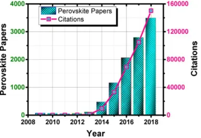
Due to this unprecedented rise in efficiency, perovskites quickly drew attention from the scientific community. Given their hybrid nature (organic A part and inorganic B part) and their uncanny electrical behaviour (J-V hysteresis), both chemists (in- and organic) and physicists took interest in these materials. The number of perovskite-related papers went from very few in 2009 to 3,500 in 2018, a rise mirrored (to an even stronger degree) by the steep increase in the number of citations from very few in 2009 up to 160,000 by 2018 (Figure 10). These two metrics highlight the excitement of the scientific community for perovskite PV.
Figure 10. Rise of perovskite research as viewed through the published papers and their citation impact over the
2009−2018 period (Source: Web of Science, Clarivate Analytics March 3, 2019)49.
Like for any other PV technology; even though the time lapse was shorter for perovskites; the increase in cell efficiency came with numbers of crucial advances along the way: new chemical compositions, new type of cells and new manufacturing processes.
48 NREL efficiency chart (version 2019-08-02) 49De Angelis (2019) ACS Energy Lett., 4, 853−4
15
i.
New perovskite compositions
Nearly half a decade after the ‘simple’ CH3NH3PbI3 and CH3NH3PbBr3 were used as
dyes35 (‘simple’ because A, B and X sites are occupied by single ions), the very first
independently certified perovskite solar cell was reported at 14.1%50 with a CH
3NH3PbI3
absorber. Few months later, a new record was set to 16.2%, this time with a mixed halide perovskite CH3NH3PbI3-xBrx51. The subsequent arrival of mixed cation perovskites was a
game changer. In 2014, CH(NH2)2+ formamidinium cation (FA) was incorporated in the A site
at the level of 85%52 and then 95%53. In 2016, Saliba et al.54 even proved the feasibility of
incorporating a third cation, simultaneously establishing a new record of 21.1% with a Cs-containing perovskite. Except for the very first one, all reported NREL-certified research perovskite solar cells are based on mixed materials (Figure 11), making it one of the key aspects for the future of this technology.
Figure 11. Evolution between 2013 and 2017 of the NREL-certified efficiencies for the best research perovskite
solar cells55 with the corresponding perovskite compositions.
Considering the 3D lattice defined by the corner-sharing PbX6 octahedra with A-filled
cavities, a relative freedom regarding the A-site cation size is allowed. In 1926, V. M. Goldschmidt rationalized an indicator accounting for the compatibility of ions within the 3D perovskite lattice56. Considering a Pb-and-I-based perovskite, it is possible to predict the
potential incorporation of a given A-cation into the network depending on the value of the calculated tolerance factor (Figure 12).
50 J. Burschka et al., (2013) Nature, 499, 316–319
51 N. J. Jeon et al., (2014) Nature Materials, 13, p 897–903 52 N. J. Jeon et al., (2015) Nature, 517 (7535), p 476-80 53 W. S. Yang et al., (2015) Science, 348 (6240) 1234-7 54 M. Saliba et al., (2016) Energy Environ. Sci., 9, 1989
55 L. K. Ono et al., (2017) ACS Appl. Mater. Interfaces, 9, 30197−246 56 V. M. Goldschmidt, (1926) Die Naturwissenschaften, 21, 477–85
16
Figure 12. Tolerance factor values for various A cations (structures are shown on the right hand side for MA, FA,
IA, EA and GA) and nature of the APbI3 crystal network (3D or non 3D)57.
Reducing mixed compositions to the sole aspect of higher efficiencies would be detrimental; they are also beneficial on other crucial levels. Incorporation of bromide for instance, enables fine tuning of the bandgap (as shown Figure 13 a). Incorporation of formamidinium or Caesium cations has been reported to increase stability of the material (as shown Figure 13 b for Cs+). Recently, addition of small amounts of Fluoride58 or Imidazolium
Iodide (C3N2H5I)59 have been reported to further increase device stability. Both aspects of
bandgap tunability and device stability being critical for the industrialization of the technology, mixed compositions unquestionably represent the future of perovskite PV.
a) b)
Figure 13. a) UV−vis absorption spectra of FTO/bl-TiO2/mp-TiO2/MAPb(I1−xBrx)3/Au cells (x ∈ [0; 1]) measured
using an integral spheres60 and b) Aging of high performance Cs
5M and Cs0M devices in a N2 atmosphere
(Csx(MA0.17FA0.83)100-xPb(I0.83Br0.17)3 perovskite abbreviated as CsxM; M for ‘mixed’)54.
ii.
New types of cells
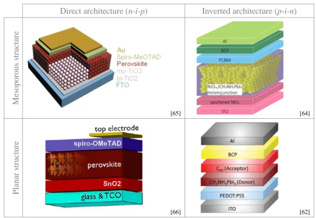
Derived from the DSSC technology, the first perovskite cells were very similar to Grätzel’s ones61 with a mesoporous structure and an Electron Transporting Layer (n-type) /
perovskite absorber (intrinsic) / Hole Transporting Layer (p-type) (from bottom to top) structure46. In 2013 Jeng et al.62 introduced a fully planar heterojunction structure with a
HTL (p) / perovskite absorber (i) / ETL (n) architecture referred to as ‘inverted’ with regard to the ‘direct’ one initially developed. Few months later, a direct planar heterojunction cell was
57 adapted from M. Saliba et al., (2016) Science, 354, 6309, 206-9 58 N. Li et al., (2019) Nature Energy, 4, 408-15
59 M. Salado et al., (2019) ChemSusChem, 12, 11 60 J. H. Noh et al., (2013) Nano Lett., 13, 4, 1764–69 61 B. O’Regan and M. Grätzel, (1991) Nature, 353, 737-40 62 J-Y Jeng et al., (2013) Adv. Mater., 25, 27, 3727-32
17 reported63. The following year, Wang et al.64 reported on an inverted mesoscopic cell. Table
1 gathers examples of these four cell types.
Direct architecture (n-i-p) Inverted architecture (p-i-n)
Me sop or ou s s tr u ct u re [65] [64] Pla na r s tr u ct u re [66] [62]
Table 1. Inventory of the different types of perovskite cells (N.B. in the top left figure: “bl” and “mp”-TiO2 stand for
“blocking layer” i.e. compact and “mesoporous” respectively).
The use of mesoscopic bottom layers involves a high temperature sintering step (usually 500°C for TiO246 and 300°C for NiOx67). With the objective of low cost devices,
scientists quickly looked into avoiding this energy-consuming step, opening the way to the planar architecture. Owing to the lower active surface (i.e. statistically less interface for e-/h+
pair dissociation), efficiencies of the planar junctions are slightly lower than those of heterojunctions.
Taking a look at the nature of the transporting layers, the direct architecture can be seen as ‘Thin Film PV’-like (with inorganic materials TiO2 and NiOx) when the inverted one is
closer to Organic PV (with PEDOT:PSS and PCBM). This differentiation echoes with the hybrid organic/inorganic nature of the perovskite material itself; stressing, once again, the rallying character of the perovskite photovoltaics field.
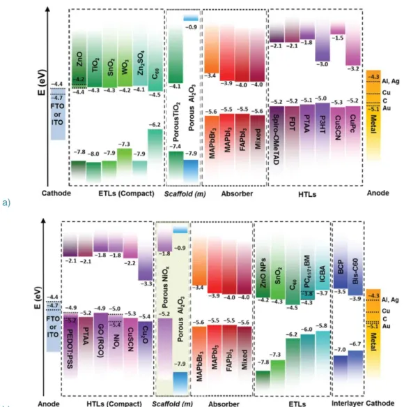
It is important to mention that while TiO2, NiOx, spiro-MeOTAD and PEDOT:PSS,
PCBM and C60 are the most widely used materials, the library for carrier-selective materials
is quite rich (Figure 14) and a dense literature on the subject can be found for both Hole68,69,70,71 and Electron72,73,74,75 Transporting Materials.
63 M. Liu et al., (2013) Nature, 501, 7467, 395-8
64 K-C. Wang et al., (2014) ACS Appl. Mater. Interfaces, 6, 15, 11851-8 65 X. Li et al., (2015) Nature Chemistry, 7, 703–11
66 M. Saliba et al., (2018) Chem. Mater., 30, 13, 4193−201 67 K. C. Wang et al., (2014) Sc. Reports, 23, 4, 4756
68 Z. Yu and L. Sun, (2015) Adv. Energy Mater., 5, 12, 1500213 69 L. Caliò et al., (2016) Angew. Chem. Int. Ed., 55, 14522-45 70 P. K. Kung et al., (2018) Adv. Mater. Interfaces, 5, 1800882
18 a)
b)
Figure 14. Energy level diagrams for a) n-i-p and b) p-i-n configurations with various Hole and Electron
Transporting Layers (H/ETL)76.
iii.
New manufacturing processes
Among the numerous advantages of perovskites, their ease of process might be one of the most striking. The first perovskites for PV were deposited by the very simple and cheap spincoating technique35: a solution containing CH
3NH3X and PbX2 (X = I-, Br-)
precursors was spincoated onto a substrate that was then annealed to form the perovskite layer. Solution-based techniques being rather cheap and simple to implement, there has been a lot of development in this field (Figure 15).
71 J. Urieta-Mora et al., (2018) : Chem. Soc. Rev., 47, 8541-71 72 H. Liu et al., (2016) Nanoscale, 8, 6209-21
73 K. Mahmood et al., (2017) RSC Adv., 7, 17044-62 74 J. Lian et al., (2018) Small Methods, 2, 1800082 75 Y. Chen et al., (2019) J. of Energy Chem., 35, 144-67 76A. Rajagopal et al., (2018) Adv. Mater., 30, 32, 1800455
19 Spincoating with antisolvent treatment77 Doctor Blade78
Two-step spincoating/dipping79 Slot die80
Inkjet printing81 Blowing-assisted drop casting82
Pressure processing method83
Sheath-gas-assisted electrospray84 Brush painting and spray coating85
Figure 15. Overview of solution-based manufacturing techniques for perovskite thin films. 77 N. J. Jeon et al., (2014) Nature Materials, 13, 897-903
78 A. T. Mallajosyula et al., (2016) Applied MaterialsToday, 3, 96-102 79 J. Burschka et al., (2013) Nature, 499, 316-9
80 J. B. Whitaker, (2018) Sustainable Energy Fuels, 2, 2442-9 81 F. Mathies et al., (2016) J. Mater. Chem. A, 4, 19207-13 82 C. Zuo et al., (2018) Nano Energy, 46, 185-92
83 H. Chen et al., (2017) Nature, 550, 92-5
84 S. Han et al., (2018) ACS Appl. Mater. Interfaces, 10, 8, 7281-8 85 A. K. Chilvery et al., (2015) J. of Photonics for Energy, 5, 053093
20 Besides the inherent varying parameters of these different techniques (ex. dispensing and coating speeds) there are numerous solution-related varying parameters. Several studies showed the impact of precursor molar ratio86, solvent(s)87 and aging88 of the
perovskite solution on the film quality. As such, there are now, for instance, almost as many recipes for spincoating processing as there are of scientists using this method.
While solution-based techniques are relatively easy to master, the large parameter plurality makes them hardly reproducible in between batches. Development of solvent-free methods has thus been undertaken. In 2013 the first vacuum-based perovskite layer for PV applications was fabricated using coevaporation process63. Further developments were made
in the field leading to two-steps processes and hybrid evaporation process (Figure 16). A non-exhaustive bibliography on vapor-deposited perovskites, published in 2016, can be found in Ono et al.89.
Coevaporation63 Sequential evaporation90
Hybrid Chemical Vapor Deposition91 Hybrid deposition92
Figure 16. Overview of vacuum-based manufacturing techniques for perovskite thin films.
Due to the volatility of the organic compound during evaporation, control over the perovskite composition is harder to get with regards to the solution process where the molar ratio is controlled from the precursor solution concentration.
86 K. Yan et al., (2015) J. Am. Chem. Soc., 137, 4460-8
87 X. Cao et al., (2019) ACS Appl. Mater. Interfaces, 11, 7639-54 88 H. Tsai et al., (2017) Adv. Energy Mater. 2017, 7, 1602159 89 L. K. Ono et al., (2016) J. Mater. Chem. A, 4, 6693-713 90 C. W. Chen et al., (2014) Adv. Mater., 26, 38, 6647-52 91 M. R. Leyden et al., (2014) J. Mater. Chem. A, 2, 18742-5 92 L. K. Ono et al., (2014) Energy Environ. Sci., 7, 3989-93
21 Adding to this already quite wide range of processing methods, perovskites thin films can also be fabricated using transfer methods. These latters combine the stoichiometric control of solution-based processes with the homogeneous and larger scale deposition features of vacuum-based processes. The first transfer method was reported in 1999 by Mitzi et al.93 that fabricated various perovskites thin films using a single source thermal ablation
process. It essentially consists in fabricating a perovskite crystal94 or film95 from solution
based techniques and, using a vacuum reactor, to flash-evaporate it onto the desired substrate (Figure 17). The heating source usually consists of a regular power supply but the use of a laser has also been reported96.
Single-source Physical Vapor Deposition94 Flash evaporation95
Laser-induced flash-evaporation printing96
Figure 17. Transfer methods for perovskite thin films.
Over the years vapor-deposited perovskite cells have been challenging solution-processed ones in terms of efficiency, with the symbolic 20% achieved by the end of 2016 (Figure 18). While they require larger and more expensive equipments, they seem nonetheless more suited than solution-based techniques for the industrialization challenge awaiting the perovskite PV technology.
93 D. B. Mitzi et al., (1999) Chem. Mater., 11, 542-4 94 P. Fan et al., (2016) Sc. Reports, 6, 29910 95 G. Longo et al., (2015) Chem. Comm., 51, 7376
22
Figure 18. Evolution between 2013 and 2017 of the best research-cell efficiencies for perovskite solar cells
obtained by solution processing or vapor deposition97.
As a matter of fact, vapor-deposition allows fabrication of homogeneous films, over large area, on any substrate (i. e. textured c-Si for tandem applications), with both high repeatability and high reproducibility which makes it very suitable for industry-scale manufacturing. The evaporation technique is, for instance, already widely implemented for OLED (Organic Light Emitting Diodes), with the examples of OLEDON98 and Universal
Display Corporation99 companies. For perovskites, with the future challenge of tandems and
particularly the c-Si-based approach, coevaporation seems even more relevant. OXFORD PV Company100, spin-out from the University of Oxford launched in 2010 by Henry
Snaith and Kevin Arthur, spearheads the development on the topic.
In this context, I was asked to implement and develop the coevaporation process for perovskite thin films for large area solar cells using a semi-industrial equipment, starting with the CH3NH3PbI3reference material. In order to better apprehend the working environment,
the next section develops all reported works on coevaporated CH3NH3PbI3.
IV.
‘Simple’ CH
3NH
3PbI
3thin films fabrication by coevaporation
The first report for a CH3NH3PbI3 thin film by coevaporation can be found in
Era et al.101 back in 1997. Using a simple dual-source evaporation setting, the authors
fabricated various perovskite films starting from RNH3I and PbI2. In this article the mention for
CH3NH3PbI3 is almost anecdotal and no further description other than a very brief « we
succeeded in preparing thin films of the cubic perovskite (CH3NH3)PbI3 » is given.
Almost twenty years later, Liu et al.63 integrated for the first time vacuum-processed
perovskites into PV devices. They used a dual-source evaporation reactor to fabricate a CH3NH3PbI3-xClx perovskite from the simultaneous evaporation of CH3NH3I and PbCl2. The
fabricated film was of higher homogeneity (flat film with a mean thickness around 330 nm) when compared to a wet-processed spincoated one (undulating film with a thickness ranging from 50 to 410 nm) (Figure 19) and led to better performing PV devices (15.4% vs. 8.6% for a spincoated perovskite film).
97 J. Avila et al., (2017) Joule, 1, 3, 432-42 98 OLEDON
99 UDC
100 OXFORD PV
23
Figure 19. Cross-section SEM images of Glass/FTO/c-TiO2/CH3NH3PbI3-xClx/Spiro-OMeTAD/Ag solar cells
constructed from vapour-deposited and solution-processed perovskite films (highlighted in red on the images)102.
Few months later, at the Instituto de Ciencia Molecular (ICMol), Malinkiewicz et al.103,
reported on the very first evaporated CH3NH3PbI3 for PV applications. The authors noticed
that the organic compound exhibited a non-directive evaporation. Upon its heating to 70°C all three quartz sensors of the chamber (one at each evaporation source and one at the substrate holder, Figure 20) gave a signal even though the PbI2 source was not running.
They found themselves unable to calibrate the MAI sensor and had to adapt their process.
Figure 20. Scheme of the dual evaporation system from ICMol team108.
They decided to first heat MAI to 70°C, waiting for its quartz sensor reading (sensor 1 on Figure 20) to be stable before heating up PbI2 and then used this latter rate as the
adjusting parameter. They determine the optimum heating temperature for PbI2 to be 250°C,
corresponding to a 0.5 Å/s deposition rate. Integrating these vacuum-processed perovskite layers into PV devices of structure ITO/PEDOT:PSS/polyTPD/perovskite/PCBM/Au they achieved at that time 12% efficiency on a 0.09 cm² device. Since then this procedure has been reported in tens of papers from the ICMol team (Table 2). Optimizing the charge transport layers, efficiencies over 20% have been achieved (on 0.01 cm² cells) with a complex fully evaporated structure114. Outside this team, only very few works on
coevaporated CH3NH3PbI3 thin films for PV applications have been reported.
A team from Seoul National University (SNU) developed a MAI-vapor-pressure-based method105. In their first paper in 2015104, Kim et al. followed ICMol’s procedure, heating MAI
up to 70°C, to reach a pressure of 2.10-5 Torr, while PbI
2 was set to a deposition rate of
102 adapted from reference [63]
103 O. Malinkiewicz et al., (2014) Nature Photonics, 8, 128-32 104 B. S. Kim et al., (2015) Org. Elec., 17, 102-6
24 0.5 Å/s (read on sensor 1, Figure 21). Over 72 samples (within 6 different batches) of ITO/MoO3/NPB/CH3NH3PbI3/C60/BCP/Al structure with a 0.04 cm² active area, the PCE
Gaussian distribution reached its peak between 11 and 12%. Their best device achieved a 13.7% efficiency.
Figure 21. Scheme of the dual evaporation system from SNU team105.
One year later, in their second paper, SNU’s team report their MAI-vapor-pressure-based method105. They varied the MAI vapor pressure from 0.6 to 8.3.10-5 Torr in between
experiments (the pressure during deposition was kept constant ± 0.1 Torr by controlling the MAI crucible temperature). They specify in this paper that « a 2 nm thick PbI2 layer was
deposited before heating up the MAI » but no mention of any temperature was made in the overall paper. We expect them to have followed, for this second paper too, the procedure developed at ICMol with the 250°C and 70°C target temperatures for PbI2 and MAI
respectively. In 2015, they had found this MAI temperature to yield a 2.10-5 Torr vapor
pressure. In their second paper where this vapor pressure is quite finely tuned (between 0.6 and 8.3.10-5 Torr), the authors unfortunately fail to provide any temperature values
corresponding to this pressure management.
Another report of coevaporated CH3NH3PbI3 was found in Lin et al.106, with very few
details provided. The authors heated the CH3NH3I precursor up to a constant 100°C and the
PbI2 temperature was varied between 250 and 280°C yielding an overall deposition rate
between 0.3 and 1.1 Å/s (monitored by a single sensor positioned between the two sources). They claim 260°C is the optimal PbI2 temperature for their evaporation configuration but fail
to provide the corresponding deposition rate. Integrating the fabricated films into perovskite devices of structure ITO/PEDOT:PSS/PCDTBT/CH3NH3PbI3/PCBM/LiF/Ag they achieved
16.5% (on 0.2 cm²), a record at that time for a non-oxide perovskite cell.
105 B. S. Kim et al., (2016) J. Mater. Chem. A, 4, 15, 5663-8 106 Q. Lin et al., (2015) Nature Photonics, 9, 106-12
25 Coevaporation conditions disclosed Photovoltaic devices ref. Structure
(if given, active area in cm²)
PCE (%)
CH3NH3I 70°C
PbI2 250°C; 0.5 Å/s
“ICMol procedure”
ITO/PEDOT:PSS/polyTPD/CH3NH3PbI3/PCBM/Au
(0.09) (0.98)
12.04 8.27
[103] ITO/PEDOT:PSS/polyTPD/CH3NH3PbI3/PCBM/Au
(0.06) 12.7 [107]
ITO/PEDOT:PSS/polyTPD/CH3NH3PbI3/PCBM/3TPYMB/Au
(0.065) (0.95)
14.8 10.9
[108] ITO/PEDOT:PSS/polyTPD/CH3NH3PbI3/Fullerene/Ba/Au
__________________________ PCBM _______________________ C60 (N/A) 15.2 14.7 [109] ITO/PEDOT:PSS/polyTPD/CH3NH3PbI3/Fullerene/Ba/Ag
__________________________ PCBM Ful________________________ PCBB . (N/A) 13.6 13.3 [110] ITO/PEDOT:PSS/polyTPD/CH3NH3PbI3/IPH/PDINO/Ag
ITO/PEDOT:PSS/polyTPD/CH3NH3PbI3/… /Ba/Ag ggg
ITO/PEDOT:PSS/polyTPD/CH3NH3PbI3/I… /PFNBr/Ag i
(N/A)
14.3 13.7 13.9
[111]
ITO/TaTm:F6-TCNNQ/TaTm/CH3NH3PbI3/C60/C60:PhIm/Ag
(0.01)
ITO/C60:PhIm/C60/CH3NH3PbI3/TaTm/TaTm:F6-TCNNQ/Au
(0.01) (0.1) 15.8 18.0 20.3 [112]
ITO/PEDOT:PSS/polyTPD/CH3NH3PbI3/IPH/PDINO/Ag
(0.01)
ITO/MoO3/TBDI/CH3NH3PbI3/IPH/PDINO/Ag
(0.01)
15.30 14.85
[113]
ITO/TiO2/C60/CH3NH3PbI3/TaTm/TaTm:F6-TCNNQ/Au
(0.01) 20.83 [114]
ITO/MoO3/HTM/CH3NH3PbI3/C60/BCP/Ag
________ITO/MoO3/m-MTDATA ________ITO/MoO3/TaTm ________ITO/MoO3/TcTa (N/A) 14.4 16.3 12.2 [115]
ITO/MoO3/HTM/CH3NH3PbI3/C60/BCP/Ag
________ITO/MoO3/TaTm ________ITO/MoO3/TPA-2,7-FLTPA-TPA ________ITO/MoO3/TPA-3,6-FLTPA-TPA (0.01) 15.9 17.1 13.9 [116]
107 C. Momblona et al., (2014) APL Mater., 2, 8, 081504
108 O. Malinkiewicz et al., (2014) Adv. Energy Mater., 4, 1400345 109 G. El-Hajje et al., (2016) Energy Environ. Sci.,9, 2286-94 110 L. Gil-Escrig et al., (2016) J. Mater. Chem. A, 4, 3667-72 111 L. Gil-Escrig et al., (2016) Organic Electronics, 37, 396-401 112 C. Momblona et al., (2016) Energy Environ. Sci., 9, 3456
113 L. Caliò et al., (2017) Solar Energy Mater. & Solar Cells, 163, 237-41 114 D. Pérez del Rey et al., (2018) J. Phys. Chem. Lett., 9, 5, 1041-6 115 B. Dänekamp et al., (2019) J. Mater. Chem. B, 7, 523-7
26
ITO/C60:PhIm/C60/CH3NH3PbI3/TaTm/TaTm:F6-TCNNQ/Au
(N/A) 18.2 [117]
TCO/MoO3/TaTm/CH3NH3PbI3/C60/BCP/Ag
(0.0651)
TCO/TiO2/C60/CH3NH3PbI3/TaTm/TPBi/MoO3/Au
(0.0651) 19.3 18.8 [118] CH3NH3I vapor pressure of 2.10-5 Torr PbI2 0.5 Å/s
ITO/MoO3/NPB/CH3NH3PbI3/C60/BCP/Al
(0.04) 13.7 [104]
CH3NH3I vapor pressure
of 5.1.10−5 Torr PbI2 0.5 Å/s
ITO/MoO3/NPB/CH3NH3PbI3/C60/BCP/Al
(0.04) 14.1 [105]
CH3NH3I 100°C
PbI2 260°C
ITO/PEDOT:PSS/PCDTBT/CH3NH3PbI3/PCBM/LiF/Ag
(0.2) 16.5 [106]
CH3NH3I vapor pressure
of 1.23.10-4 mbar
PbI2 3 Å/s
FTO/TiO2/CH3NH3PbI3/Spiro-MeOTAD/Au
(0.16) 13 [119]
CH3NH3I vapor pressure
of 5.10-5 Torr
PbI2 0.75 Å/s
FTO/C60/CH3NH3PbI3/Spiro-OMeTAD/Au
(0.08) 15.7 [120]
CH3NH3I 0.4 Å/s
PbI2 0.4 Å/s
FTO/c-TiO2/CH3NH3PbI3/Spiro-OMeTAD/Ag
FTO/C60/CH3NH3PbI3/Spiro-OMeTAD/Ag
FTO/ c-TiO2/PCBM/CH3NH3PbI3/Spiro-OMeTAD/Ag
FTO/poly-TPD/CH3NH3PbI3/PCBM/BCP/Ag
(0.0919) 15.8 15.4 13.6 12.6 [121]
Table 2. Summary of reported coevaporated CH3NH3PbI3 perovskite thin films for PV applications.
It is worth noting that except two reports for ~ 1 cm² active area cell and two for 0.2 cm², all cells are well below 0.1 cm². Another striking fact is the lack of consistency in the disclosed deposition conditions: no mention of temperature for some papers and no mention of rates for others. It appears clear from this literature review that pressure is a key parameter of the coevaporation process.
With less than 20 papers found on coevaporated CH3NH3PbI3 films for PV
applications since 2013, the topic of the present thesis seems rather far from the raging ‘war’ of other perovskites-related subjects.
117 D. Kiermasch et al., (2019) J. Mater. Chem. A, 7, 14712-22
118 D. Pérez del Rey et al., (2019) Chem. Mater. DOI: 10.1021/acs.chemmater.9b01396 119 J. Teuscher et al., (2015) ChemSusChem, 8, 3847-52
120 D. Zhao et al., (2016) Nano Energy, 19, 88-97