HAL Id: hal-02306907
https://hal.archives-ouvertes.fr/hal-02306907
Submitted on 7 Oct 2019
HAL is a multi-disciplinary open access
archive for the deposit and dissemination of
sci-entific research documents, whether they are
pub-lished or not. The documents may come from
teaching and research institutions in France or
abroad, or from public or private research centers.
L’archive ouverte pluridisciplinaire HAL, est
destinée au dépôt et à la diffusion de documents
scientifiques de niveau recherche, publiés ou non,
émanant des établissements d’enseignement et de
recherche français ou étrangers, des laboratoires
publics ou privés.
An Augmented OxRAM Synapse for Spiking Neural
Network (SNN) Circuits
Hassen Aziza, H. Bazzi, J. Postel-Pellerin, P. Canet, M. Moreau, A. Harb
To cite this version:
Hassen Aziza, H. Bazzi, J. Postel-Pellerin, P. Canet, M. Moreau, et al.. An Augmented OxRAM
Synapse for Spiking Neural Network (SNN) Circuits. 2019 14th International Conference on
De-sign & Technology of Integrated Systems In Nanoscale Era (DTIS), Apr 2019, Mykonos, France.
�10.1109/DTIS.2019.8735057�. �hal-02306907�
XXX-X-XXXX-XXXX-X/XX/$XX.00 ©20XX IEEE
An Augmented OxRAM Synapse for Spiking
Neural Network (SNN) Circuits
H. Aziza1, H. Bazzi1,2, J. Postel-Pellerin1, P. Canet1, M. Moreau1, A. Harb3 1Aix Marseille Univ, Univ Toulon, CNRS, IM2NP, Marseille, France
2Lebanese International University, Department of Electrical and Electronics Engineering, Beirut, Lebanon 3The International University of Beirut, Department of Electrical and Electronics Engineering, Beirut, Lebanon
Abstract— In this paper, the conductance modulation of
OxRAM memristive devices is evaluated based on experimental data to reveal the memristor inherent analog synaptic behavior. Simulation results are presented to validate the use of OxRAMs as synapses at a circuit level in a spiking neural network context. In the proposed approach, the OxRAM synapse is augmented with a shift register associated with current compliance control transistors to provide an efficient monitoring of the OxRAM conductance.
Keywords— Memristor; Neuromorphic circuits; OxRAM; Synapses; CMOS neurons, Neural networks
I. INTRODUCTION
Traditional computing technology based on the Von Neumann architecture is facing fundamental limits such as poor energy efficiency and latency [1]. This is particularly true when dealing with the vast amount of data generated by IoT devices, self driving cars, cloud computing etc. [2]. This situation known as the “memory wall” encourages the investigation of different processing information paradigms considered as non-Von Neumann (non-VN) architectures [3]. Over the last few years there has been a lot of activity across research groups proposing efficient hybrid “CMOS-nanodevice” computing hardware architectures such as Artificial Neural Networks (ANNs) [4]. Indeed, ANNs have demonstrated impressive performances in recognition tasks where classical VN hardware architectures have difficulties to classify or organize data, something that the human brain seems to accomplish effectively.
ANNs are meant to mimic biological neural networks. ANNs architectures are based on a large collection of units that are interconnected in some pattern to allow communication between the units. These units are referred to as nodes or neurons. Every node is connected with other neurons through a connection link or synapse associated with a weight. Weights usually excite or inhibit the signal that is being communicated over the network. Thus, ANN can be seen as a complex adaptive system, which can change its internal structure based on the information passing through it [5]. Fig. 1a presents a basic ANN unit which comprises several synapses and neuron blocks. As depicted in Fig. 1b, synapse receives spikes, also known as Action Potentials (AP) from other neurons (pre-spikes) and converts them into current according to their synaptic strength. The neuron integrates these current inputs injected into it to change its internal voltage potential Vmem. Once Vmem crosses a firing threshold
Vthr, the neuron fires and sends a spike to post-synaptic and
synaptic neurons. The process of sending spikes to pre-synaptic neurons is known as back propagation.
Emerging Back-End Of Line (BEOL) resistive memory devices are considered as the optimum candidates to emulate
biological synaptic behavior at nanometer scale as they offer the possibility to modulate their conductance in addition to being easily integrated with CMOS-based neuron circuits [6][7]. Among these emerging technologies, Oxide-based RAM (so called OxRAM) have proven to be very effective in implementing some aspects of synaptic plasticity [8].
(a) (b) Fig. 1. Spiking neural network neuromorphic model.
In this paper, we present how OxRAM memory devices can be used for synaptic plasticity functions by simply controlling the current flowing through the cell. In Section II, OxRAM technology is presented along with memristor-based neural networks basic concepts. In Section III, the ability of the OxRAM cell to be used as a synapse is presented based on experimental results. In Section IV, simulation results are proposed to validate the concept, while Section IV presents concluding remarks.
II. BACKGROUND
A. OxRAM technology
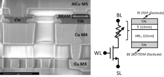
A typical Resistive RAM (RRAM) device consists of two metallic electrodes that sandwich a thin dielectric layer serving as a permanent storage medium. This Metal-Insulator-Metal (MIM) structure can be easily integrated in the BEOL in combination with advanced CMOS technologies as presented in Fig. 2(a). The RRAM structure is integrated on top of Metal 4 copper layer (Cu). A TiN Bottom Electrode (BE) is first deposited. Then, a 10nm-HfO2/10nm-Ti/ TiN
stack is deposited to form a capacitor-like structure [9]. Fig. 2(b) shows the basic 1T1R memory cell. In this configuration one MOS transistor is placed in series with one OxRAM cell. This select transistor acts as a compliance device, limiting the amount of current passing through the cell according to its gate voltage value.
Fig. 3(a) and 3(b) present 1T1R OxRAM I-V characteristics measurements made on actual OxRAM devices in linear scale and logarithmic scale respectively. Based on I-V curves, the memory cell operation can be seen as follow: after an initial electroforming step (not presented here), the memory element
Neuron Neuron Pre-spikes (spikes from previous neurons) Neuron Post-spikes Pre-spikes Post-Spike Soma Synapse
can be reversibly switched between a High Resistance State (HRS) and a Low Resistance State (LRS). Resistive switching in an OxRAM element corresponds to an abrupt change between a HRS and a LRS. This resistance change is achieved by applying specific voltage across the cell (i.e. VSET and
VRESET). According to Fig. 3(a), VSET value required to switch
from HRS to LRS state is around 0.55 V, while VRESET value
required to switch back to the HRS state is around -0.75 V. Note that Fig. 3(b) is the classical log representation of the OxRAM I-V hysteresis which provides an amplification of low current values.
(a) (b) Fig. 2. (a) TEM cross-section of an OxRAM device co-integrated in a 130nm CMOS process [9] (b) Symbol view of a basic 1T1R OxRAM cell.
(a) (b) Fig. 3. I-V characteristics of an OxRAM in (a) linear and (b) log scale. SET (blue) and RESET (red) operations are highlighted.
B. Synapses
The synapse is a crucial element in biological neural networks, but a simple electronic equivalent is not possible, thus complicating the development of hardware that reproduces biological architectures. However, the recent progress in the experimental realization of memristive devices has reinforced the interest in ANNs as these devices have the ability to mimic brain synapses. Memristive devices and especially OxRAMs have demonstrated the ability to be used as a synapse within hybrid analog circuits [10]. Indeed, since the conductance of OxRAMs can be electrically and incrementally increased or decreased, it is a potential candidate for realizing an electronic equivalent of a biological synapse. In the rest of the paper, analog synapses are described in a first approximation as a tunable linear conductance, defining the synaptic weight between two neurons.
C. Neurons
One of the simplest artificial neuron model is the “Integrate and Fire” (IF) neuron model [11]. In this model, neuronal dynamics can be conceived as an integration process combined with a mechanism that triggers spikes above some critical voltage. As the shape of spikes is always the same, information is contained in the presence or absence of a spike.
Therefore, spikes are reduced to ‘events’ that happen at a precise moment in time, introducing the concept of Spiking Neural Networks (SNNs). Neuron models where action potentials are described as events are called IF models. Fig. 4 shows the model of a simple IF neuron. It sums over time (integrates) the incoming excitatory signals inside the neuron integration block using a capacitor. This capacitor models the neuron cell membrane. The integration process leads to an increase in the cell membrane potential of the neuron Vmem.
When Vmem reaches the threshold value Vthr, the neuron
generates an output spike. After the neuron has fired the membrane potential is restored to a resting value. Because the cell membrane is not perfect, the charge will, over time, slowly leak through the capacitor, introducing the concept of Leaky Integrate and Fire neurons (LIF). In Fig. 4, the “leaky” behavior is modelled by a resistor Rleak in parallel with the
capacitor Cmem.
Fig. 4 Basic working operation of a Leaky Integrate and Fire neuron (LIF).
D. Neuromemristive systems
Neuromemristive systems (NMSs) are based on a design approach with closely coupled resistive memory and processing, resulting in high area and energy efficiency. Neuromemristive network topology that has been mostly investigated in the literature is the fully connected neural network [12]. In this configuration, each neuron of a layer is connected to every neuron of the previous layer, as presented in Fig. 5(a). This general purpose connection pattern is very expensive in terms of connections sine each neuron gathers inputs from thousands of synapses to decide when to produce a spike, which limits the maximum number of hidden layers to one or two. In contrast, in a convolutional network, depicted in Fig. 5(b) (also referred to as deep neural networks [13]), each neuron receives inputs from some number of locations in the previous layer. (i.e. each neuron is only connected to a few nearby neurons). This connection pattern allows a cascade of many layers and only makes sense for cases where the data can be interpreted as spatial, which is the case for visual pattern recognition applications.
(a) (b)
Fig. 5 (a) Fully connected neural network and (b) convolutional network where a small set of synapses is shared among different neurons to connect layer N and N+1. WL SL BL TE (TOP Electrode) BE (BOTTOM Electrode) Hf02(10nm) Ti (10nm) TiN TiN output layer hidden layer (N+1) input Layer (N)
III. OXRAMCONDUCTANCE MODULATION
A recent advance in the field of OxRAM memories is related to Multi Level Cell operation (MLC) [14]. According to this approach, more than two data states are made possible for each memory cell, simply by finely controlling the programming of the cell. Thus, the OxRAM can be considered as a time varying resistor. At a circuit level, different implementations of MLC operation are adopted. Multilevel operation can be achieved by:
- Applying an increasing number of identical voltage to the OxRAM BL node. In this case, LRS level is function of the number of pulses [15].
- Modulating directly the SET voltage level generated from the SET decoder. In this case, LRS levels are achieved with different SET voltage values [16].
- Modulating the compliance current of the memory cell during SET, which can be achieved by controlling the gate voltage (WL) of the select transistor [17].
The first approach requires a pulse generator while the two others require analog voltage levels generated from a specific circuitry.
In this work, the compliance current modulation technique is adopted to reach different LRS levels. To validate this approach, a set of measurements are performed. Table I presents the different voltage levels applied across the OxRAM cell presented in Fig. 6(a) during RESET, SET and READ operations. During RESET a negative voltage ramp is applied on BL node down to -1.2V with WL set to 4V while the SL node is grounded. During SET, a positive voltage ramp is applied on BL node up to 1.2V for three different gate voltage levels WLequal to 1.2V, 1.6V and 2V, resulting in three different compliance currents and three different LRS values. These results are extracted from Fig. 6(b). After an initial RESET operation, three SET operations are performed for increasing WL voltage values. Note that no RESET operation is achieved between the SET operations. The whole process is repeated 10 times to reproduce the OxRAM behavior. As a result, three distinct resistance levels equal to 2.50 kΩ, 1.45 kΩ and 1.12 kΩ are obtained, showing the ability of the memory cell to store different RLRS values
according to the gate voltage bias. Note that RHRS/LRS values
presented in Table I are averaged over 10 measurements.
TABLE I. PROGRAMMING VOLTAGES AND CORRESPONDING RESISTANCE VALUES
RESET SET READ WL 4V 1.2V 1.6V 2V 4V BL -1.2V 1.2V 1.2V 1.2V 0.1V SL 0V 0V 0V 0V 0V
RHRS/LRS 320 kΩ 2.50 kΩ 1.45 kΩ 1.12 kΩ -
(a) (b)
Fig. 6 I-V (a) OxRAM cell external nodes (b) I-V characteristic of an OxRAM after 10 RESET and SET cycles for different WL voltages.
In a second step, to obtain a tunable resistance, the gate voltage bias applied to WL node is changed incrementally. Fig. 7(a) presents the evolution of RLRS resistance for different
gate voltage levels ranging from 0.6V to 2.5V with a 0.1V voltage step. In Fig. 7(b), an area of interest is highlighted where gate voltage levels range from 1.1V to 2V. This area will be exploited to modulate the OxRAM conductance in a SNN circuit context.
Fig. 7 (a) Evolution of the LRS resistance according to WL voltage values ranging from 0.6V to 2.5V (b) area of interest with WL voltage values ranging from 1.1V to 2V.
IV. AUGMENTED OXRAM SYNAPSE
The presented CMOS synapse leverage on OxRAM compliance current control. To implement this technique at a circuit level, several transistors arranged in parallel are connected in series with an OxRAM cell. Hence, instead of controlling a larger single transistor with a variable control gate voltage, transistors are activated successively in order to monitor the compliance current of the cell.
Fig. 8 presents the proposed CMOS synapse model implementation. The synapse is modelled by one OxRAM cell, a 5-bit shift register and four transistors. The control of the current flowing through the OxRAM cell is achieved by controlling the gate of transistors M0 to M3. This topology can be used to increment (synapse weight is increased) or decrement (synapse weight is decreased) the OxRAM conductance during SET operation.
The shift register, detailed in Fig 9(a) is in charge of the activation of the transistors. It is a serial to parallel shift register where individual data latches are all driven by a common signal called “spike” making them synchronous devices. In this application example, IN data is kept to logic ‘1’. The shift register operation is depicted in Fig 9(b). The input is shifted in the right direction after each spike, activating QX outputs. Note that the shift register is provided
with a “reset” connection used to reset all QX outputs to ‘0’
after the fifth spike. “reset” signal is also used to trigger a RESET operation: in this case, the pulse generator is grounded and the source nodes of M0 to M3 transistors are connected to
WL SL BL Icell (a) (b)
a RESET pulse generator. The number of individual data latches required to make up the shift register can be increased (or decreased) to refine (or relax) the control of the OxRAM conductance value. As a consequence, the number of transistors would also increase (or decrease) in the same order. The memory cell is modelled by an Oxide-based RRAM model fully calibrated on silicon for a TiN/Ti/HfO2/ TiN
RRAM stack [18]. The OxRAM technology is integrated within a 130nm CMOS High Voltage technology from ST-Microelectronics. Regarding the design rules, the minimal transistor size is considered for MX transistors.
Fig. 8 Proposed hybrid synapse circuit.
(a)
(b)
Fig. 9 (a) 5-bit serial-in to parallel-out shift register (b) data outputs versus spike activity.
In this approach shift registers are used as volatile data storage nodes used to update the non OxRAM conductance which stores synaptic weights. The OxRAM combined with a shift register can have several applications in a SNN context. The movement of data within the shift register can be triggered by pre-synaptic neuron spikes according to the targeted SNN architecture and learning mechanism. Also, a parallel-in to parallel-out shift register can be used to update synaptic weights from outside (initialization of the synaptic weights of a SNN before the learning process).
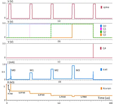
Transient simulation results are presented in Fig. 10. Spikes are generated without any interruption (Fig. 10a). Spikes are
represented by square pulses for simplicity. However, any shape of signal can be considered (including signals suited to spike-timing-dependent plasticity learning rule) provided that its maximum value triggers the shift register.
After each spike, the shift register outputs Q0 to Q3 switch successively from a low to a high level (Fig. 10b). After the fifth spike, Q4 rises and instantly resets the shift register (Fig. 10c). As Q0 to Q3 signals control respectively M0 to M3 transistors, the current Icell flowing through the OxRAM
increases incrementally (Fig. 10d) according to the decrease of the OxRAM resistance (Fig. 10e).
Fig. 10 Transient simulation results showing the evolution of the OxRAM resistance according to the current compliance limit set by MX transistors. As already mentioned, the number of transistors used to limit the current flowing through the OxRAM cell can be increased to finely tune the LRS resistance, but at the cost of increasing the synapse size in terms of transistors. Moreover, several flavors of shift registers with clear or reset connections can be used in order to increase but also decrease the OxRAM conductance. For this last case, outputs CX of Fig. 9(a) can be
considered. Another way to control the resistance variation is to change the spike voltage maximum level. Indeed, small spike voltage levels will slow down the resistance change. Conversely, high voltage levels will induce a sharp change of the resistance.
V. CONCLUSION
An OxRAM conductance modulation technique based on SET current modulation is investigated to propose an augmented OxRAM synapse for SNN applications. In addition to the OxRAM cell, the proposed synapse circuit includes a shift register associated with four transistors. The circuit can be tuned (by adjusting shift register size) to provide an accurate control the OxRAM conductance.
ACKNOWLEDGMENT
The authors wish to acknowledge the support from the CEA-Leti (“Commissariat à l'énergie atomique-Laboratoire d'électronique et de technologie de l'information”). CEA-Leti
Time (us) 0 R (kΩ) I (mA) V (V) V (V) V (V) 1.0 71 kΩ 3,37 kΩ 2,47 kΩ 1,75 kΩ 1,73kΩ 0.5 0 3.3 0 3.3 0 3.3 0 (a) (b) (d) (e) 100 (c) 5 M0 M1 M2 M3 0
provided the technology access as part of the Memory Advanced Demonstrators project (MAD200).
REFERENCES
[1] E. Linn et al., “logic operations in passive crossbar arrays alongside memory operations, Nanotechnology,” 23(30), 305205, 2012. [2] R. Aitken et al, “Device and technology implications of the Internet of
Things,” Symposium on VLSI Technology (VLSI-Technology): Digest of Technical Papers, Honolulu, HI, 2014, pp. 1-4, 2014. [3] S. Hamdioui et al., “Memristor for computing: Myth or reality?”, In
Proceedings of the Conference on Design, Automation & Test in Europe, pp. 722-731, 2017.
[4] C. Gamrat et al., “The architecture of mind neurocomputers”, in MicroNeuro Int. Conf. on Microelectronics for Neural Networks, Munich, Germany, 1991, pp. 463–469.
[5] Guo-qiang Bi and Mu-ming Poo, “Synaptic modifications in cultured hippocampal neurons: dependence on spike timing, synaptic strength, and postsynaptic cell type”, The Journal of neuroscience, vol. 18, no. 24, pp. 10 464–10 472, 1998.
[6] E. I. Vatajelu et al., “Nonvolatile memories: Present and future challenges”, In Design & Test Symposium (IDT), 2014 9th International, pp. 61-66. IEEE, 2014.
[7] S. Hamdioui e al., “Memristor based memories: Technology, design and test”, In Design & Technology of Integrated Systems In Nanoscale Era (DTIS), 9th IEEE International Conference On, pp. 1-7. IEEE, 2014.
[8] S. Yu et al., “Stochastic learning in oxide binary synaptic device for neuromorphic computing”, Frontiers Neurosci., vol. 7, pp. 186, Oct. 2013.
[9] E. Vianello et al., “Resistive Memories for Ultra-Low-Power embedded computing design,” IEEE International Electron Devices Meeting (IEDM), 2014.
[10] J.M. Portal et al., “Design and Simulation of a 128 kb Embedded Nonvolatile Memory Based on a Hybrid RRAM (HfO2)/28 nm FDSOI CMOS Technology,” IEEE Transactions on Nanotechnology, 16(4), pp.677-686, 2017.
[11] G. Indiveri et al., “Neuromorphic silicon neuron circuits”, Frontiers in neuroscience, vol. 5, 2011.
[12] D. E. Rumelhart et D. Zipser, “Feature discovery by competitive learning,” Cognitive Science, 9(1):75–112, 1986.
[13] P. Simard et al., “Best practices for convolutional neural networks applied to visual document analysis,” In Seventh International Conference on Document Analysis and Recognition, Proceedings., volume 1, p. 958–963, 2003.
[14] H. Aziza et al., “Multilevel Operation in Oxide Based Resistive RAM with SET voltage modulation”, IEEE Proceedings of International Conference on Design & Technology of Integrated Systems in Nanoscale Era (DTIS), Istanbul, Turkey, April 12-14, pp. 1-5, 2016. [15] H. Aziza et al., “RAMs as Analog Trimming Elements” – Journal of
Solid-State Electronics, vol. 142, pp. 52-55, 2018.
[16] H. Aziza et al., “Impact of Line Resistance Combined with Device Variability on Resistive RAM Memories”, Journal of Advanced Science Technology Engineering Systems, vol. 3, no.1, pp. 11-17, 2018.
[17] W. Chen et al., “Switching characteristics of W/Zr/HfO2/TiN ReRAM devices for multi-level cell non-volatile memory applications”, Semiconductor Science and Technology. 30. 10.1088/0268-1242/30/7/075002, 2015.
[18] Bocquet et al., “Robust compact model for bipolar oxide-based resistive switching