HAL Id: hal-02413833
https://hal.archives-ouvertes.fr/hal-02413833v2
Submitted on 9 Nov 2020HAL is a multi-disciplinary open access archive for the deposit and dissemination of sci-entific research documents, whether they are pub-lished or not. The documents may come from teaching and research institutions in France or abroad, or from public or private research centers.
L’archive ouverte pluridisciplinaire HAL, est destinée au dépôt et à la diffusion de documents scientifiques de niveau recherche, publiés ou non, émanant des établissements d’enseignement et de recherche français ou étrangers, des laboratoires publics ou privés.
Design of AlGaN/AlN Dot-in-a-Wire Heterostructures
for Electron-Pumped UV Emitters
Ioanna Dimkou, Anjali Harikumar, Akhil Ajay, Fabrice Donatini, Edith
Bellet-Amalric, Adeline Grenier, Martien den Hertog, Stephen Purcell, Eva
Monroy
To cite this version:
Ioanna Dimkou, Anjali Harikumar, Akhil Ajay, Fabrice Donatini, Edith Bellet-Amalric, et al.. Design of AlGaN/AlN Dot-in-a-Wire Heterostructures for Electron-Pumped UV Emitters. physica status solidi (a), Wiley, 2020, 217 (7), pp.1900714. �10.1002/pssa.201900714�. �hal-02413833v2�
1
This is the accepted version of the following article: [I. Dimkou, A. Harikumar, A. Ajay, F. Donatini, E. Bellet-Amalric, A. Grenier, M.I. den Hertog, S. Purcell, E. Monroy.
Design of AlGaN/AlN Dot-in-a-wire Heterostructures for Electron-Pumped UV Emitters, Physica Status Solidi A, 1900714 (2019)], which has been published in final form at [https://doi.org/10.1002/pssa.201900714]. This article may be used for non-commercial purposes in accordance with Wiley Terms and Conditions for Use of Self-Archived Versions.
Design of AlGaN/AlN dot-in-a-wire heterostructures for electron-pumped UV emitters
Ioanna Dimkou, Anjali Harikumar, Akhil Ajay, Fabrice Donatini, Edith Bellet-Amalric, Adeline Grenier, Martien I. den Hertog, Stephen T. Purcell, and Eva Monroy*
I. Dimkou, Dr. A. Grenier
Univ. Grenoble-Alpes, CEA-Leti, 17 av. des Martyrs, 38000 Grenoble, France
A. Harikumar, Dr. A. Ajay, Dr. E. Bellet-Amalric, Dr. E. Monroy
Univ. Grenoble-Alpes, CEA-IRIG-DEPHY-PHELIQS, 17 av. des Martyrs, 38000 Grenoble, France
E-mail: eva.monroy@cea.fr
Dr. F. Donatini, Dr. M. I. den Hertog
Univ. Grenoble-Alpes, CNRS-Institut Néel, 25 av. des Martyrs, 38000 Grenoble, France
Dr. S. T. Purcell
Univ. Lyon, Université Claude Bernard Lyon 1, CNRS, Institut Lumière Matière, 69622 Lyon, France
Keywords: ultraviolet, nanowires, AlGaN, quantum dot, lamp
This paper describes the fabrication of nitrogen-polar AlxGa1-xN/AlN (x = 0, 0.1) quantum dot
superlattices integrated along GaN nanowires for application in electron-pumped UV sources.
The nanowires are grown using plasma-assisted molecular-beam epitaxy on n-type Si(111)
wafers using a low-temperature AlN nucleation layer. Growth conditions are tuned to obtain a
high density of non-coalesced nanowires. To improve the uniformity of the height along the
substrate, the growth begins with a base long nanowire (~900 nm), with a diameter of 30-50
nm. The AlxGa1-xN/AlN active region is 400 nm long (88 periods of quantum dots), long enough
to collect the electron-hole pairs generated by an electron beam with an acceleration voltage
2
thickness ratio and the Al content in the dots. Internal quantum efficiencies as high as 63% are
3
1. Introduction
UV light emitting diodes (LEDs) are in demand for disinfection purposes [1] at specific
wavelengths. They also offer lower power consumption, the potential for longer lifetime, lower
voltage requirement and non-toxic waste after use, as opposed to their mercury lamp
counterparts. AlGaN is the material of choice for this technology because of its direct bandgap
and the possibility to dope it both n-type and p-type [2,3]. Having said that, such devices have
not reached their industrial maturity yet due to drawbacks in terms of electrical injection and
light extraction, which limit their wall-plug efficiency (WPE) [4]. Let us remind that the WPE
is the ratio between the optical output power and the electrical input power. WPE can be written
as WPE = LEE × IQE×EIE, where LEE is the light extraction efficiency, IQE is the internal
quantum efficiency (number of photons generated per electron-hole pair injected in the active
medium), and EIE is the electron injection efficiency.
A promising alternative for the fabrication of highly efficient, eco-friendly UV lamps is
based on the injection of electrons into AlGaN/AlN nanostructures using a miniaturized
electron gun, e.g. a carbon nanotube cathode. An electron-pumped device looks like a vacuum
tube or valve [5], which can be scaled down to millimeter size. Such a configuration avoids the
problems associated with the carrier injection (dopant ionization energy, asymmetric carrier
mobility of electrons and holes, realization of ohmic contacts). In the case of pumping with an
electron beam, the average energy required to generate an electron-hole pair in a given
semiconductor is close to 3 times its band gap energy [6]. Therefore, the electron injection
efficiency is wavelength independent (EIE » 1/3), and it should be possible to fabricate lamps operating close to the AlN band gap (e.g. 210 nm) if the IQE and LEE of the emitting structure
is high enough. . In the spectral range generally used for disinfection, implantation of such a
4
become comparable to LEDs thanks to the higher device output power (easily scalable with the
semiconductor surface) and simpler material growth and processing.
Electron-pumped emission from GaN and AlGaN quantum wells has been reported [7–12],
but such lamps displayed low wall plug efficiency mostly due to the poor light extraction
efficiency. Furthermore, stimulated emission around 350 nm has been demonstrated in
electron-pumped GaN/AlGaN ridge structures under pulsed pumping [12–14]. For the
implementation of such electron-pumped UV sources, the semiconductor geometry and
conductivity must be adapted to maximize the energy conversion, light extraction and charge
evacuation. There are several motivations to consider nanowires (NWs) for this application.
First, their as-grown shape spontaneously favors light extraction [15], without additional
processing requirements. In addition, the relatively easy implementation of three dimensionally
confined objects (dots in a wire) results in high values of internal quantum efficiency (IQE) at
room temperature [16]. Last but not the least, their direct growth self-assembled on silicon
substrates reduces the cost of the system.
One of the main challenges for the growth of NW ensembles for electron-pumped UV
sources is the homogeneity of the dot thickness and composition along an active region that is
hundreds-of-nm long. It is known that the luminescence from GaN/AlGaN and AlGaN/AlN
superlattices (SLs) on GaN NWs presents strong spectral dispersion, with broad and sometimes
multi-line spectral profiles [17,18]. Such dispersion is due the variation of the dot height and
diameter along the growth axis [19–21], the different strain relaxation in the dots along the growth
axis [19,20,22], the presence of monolayer thickness fluctuations in the dots [19], and the alloy
inhomogeneities and inter-diffusion phenomena at the hetero-interfaces, which depend on the
strain state of the structure [18]. Additional perturbations can be introduced by coalesced areas
and lateral GaN inclusions [23]. It is hence highly important to develop precisely controlled
growth processes that allow the synthesis of homogeneous AlGaN/AlN quantum dot SLs in a
5
In this work, we describe the growth and characterization of N-polar AlxGa1-xN/AlN (x=0,
0.1) quantum dot SLs grown as extensions on GaN NWs and designed for their application in
electron-pumped UV sources. The NWs are grown using plasma-assisted MBE on n-type
Si(111) wafers using a low temperature AlN nucleation layer. Growth conditions are tuned to
obtain a high density of non-coalesced GaN NWs. On top of them, the AlxGa1-xN/AlN active
region is 400 nm long (88 periods of quantum dots). Such structures present single-line spectral
emission with IQE that can reach 63%.
2. Results and discussion
Self-assembled N-polar GaN NWs were synthesized using plasma-assisted molecular beam
epitaxy (PAMBE) on n-type Si(111) substrates using a low-temperature AlN nucleation layer,
as described elsewhere [24,25]. To improve the height uniformity [26], the growth began with a
long (~900 nm) NW base with a diameter of 30-50 nm, grown under N-rich conditions (Ga/N
flux ratio: FGa/FN = 0.25) at a substrate temperature TS = 810°C and at a growth rate
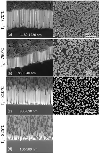
vG = 290 nm/h. The choice of growth conditions is based on the study described in figure 1.
From these bird’s eye and top-view scanning electron microscopy (SEM) images, we observe
that increasing the substrate temperature from 770°C to 810°C results in a reduction of the NW
density, at the price of a slight decrease of the growth rate due to the enhancement of GaN
decomposition. However, at 825°C the decomposition rate is too high, and the NW height
becomes highly inhomogeneous.
The growth of the GaN base was followed by the deposition of a 400-nm-long AlxGa
1-xN/AlN (x = 0, 0.10) SL, i.e. 88 periods of quantum dots. The AlxGa1-xN dots were grown using
the same Ga flux as for the NW base, and adding an Al flux FAl = x/vG, where x is the targeted
Al mole fraction. The AlN sections were grown at the stoichiometry (FAl/FN = 1). The whole
6
the dot/barrier thickness ratio and the Al content in the dots, maintaining the number of periods
(88) and the period length (4.5 nm) constant. The values of Al mole fraction in the dots given
in this manuscript are nominal values. From the position of the (0002) reflection of the quantum
dot SL in x-ray diffraction studies we estimate that the error bar in the composition is in the
range of ± 2%. The Al mole fraction in the AlxGa1-xN dots was kept intentionally low, around
x = 0.1, to prevent deformations of the nanowire morphology and reduce the effects of alloy
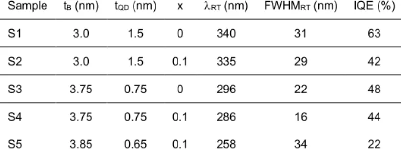
inhomogeneities, observed for x ≥ 0.3 [18]. The nominal characteristics of the samples presented
here are listed in table 1.
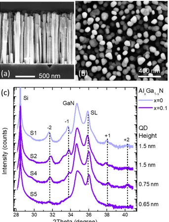
Figures 2(a) and (b) present typical (a) cross-section and (b) top-view SEM images of an
as-grown sample of GaN NWs containing an AlxGa1-xN/AlN SL, e.g. the image corresponds to
a sample with 88 periods of Al0.1Ga0.9N / AlN (sample S4). The NWs are detached from each
other, but highly packed. Top view images point to a NW density of 6-8×109 cm-3. The NW
diameter is in the range of 30-50 nm at the base, increasing to 50-70 nm in the top region due
to the enhancement of lateral growth when depositing AlN [27,28].
The as-grown NW ensemble was characterized using XRD in order to validate the
periodicity of the structure, with the results illustrated in Figure 2(c). These measurements
provide average information over a surface of several millimeters squared, and are hence
sensitive to the dispersion of tilts and twists in the NW ensemble. Several satellites of the (0002)
reflection of the SL are resolved, which confirms the thickness uniformity along the growth
axis and the reproducibility of the period length from sample to sample (period = 4.3±0.2 nm).
It should be noticed that the (0002) reflection of GaN originated by the NW base is not located
at the angular position of relaxed GaN (2q = 34.57°), but at slightly larger angles.
To get highly resolved information on the NW structure, the NWs were dispersed on holey
carbon membranes for scanning transmission electron microscopy (STEM) observations.
Figure 3(a-b) presents high-angle annular dark field (HAADF) STEM images of a GaN/AlN
7
along the NW, and the whole GaN/AlN SL is enveloped by an AlN shell. Figure 3(c) shows a
high magnification HAADF-STEM view of an Al0.1Ga0.9N/AlN (0.65 nm / 3.85 nm) SL
(sample S5), which confirms the nominal layer thicknesses and the homogeneity of the structure.
In both samples, we observe a decrease of the thickness of the AlN shell along the growth axis,
which is more important in the sample with higher Al content in the SL. This is consistent with
the fact that the AlN shell forms as a result of the low mobility and of the Al atoms impinging
on the NW sidewalls. From STEM analysis of various NWs, the thickness of the shell is
estimated to be only 1-2% of the axial AlN thickness. The presence of the AlN shell imposes a
uniaxial compressive stress to the GaN base, which justifies the shift of the GaN (0002) XRD
reflection as observed in Figure 2(c).
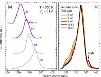
Optical characterization by cathodoluminescence (CL) at room temperature, with an
electron acceleration voltage VA = 5 kV, is presented in Figure 4(a). The emission blue shifts
when we decrease the dot height and increase their Al content. A spectral shift from 340 nm to
260 nm is demonstrated while maintaining approximately the same spectral linewidth. The
acceleration voltage (VA) determines the penetration depth of the electrons in the structure,
which depends mostly on the material density [6]. The thickness of the SL was initially decided
by assuming that the sample behaves similar to a planar structure with the same geometry along
the growth axis. However, in a NW ensemble, the average material density is smaller, and there
is a risk of electron channeling when the direction of impinging electrons is perpendicular to
the silicon substrate. To assess the relevance of these phenomena, we have studied the variation
of the CL spectra as a function of VA, as shown in Figure 4(b). If the emission spectra are
normalized to their maximum, the emission from the GaN base becomes visible only for VA >
5 kV. This implies that the NW ensemble is compact enough to prevent important deviations
of their behavior with respect to planar structures.
Finally, we have assessed the IQE of the samples by analyzing the variation of their
8
Figure 5(a) displays the evolution of the PL spectrum as a function of temperature for a sample
containing an Al0.1Ga0.9N/AlN (0.75 nm / 3.75 nm) SL (sample S4). Figure 5(b) depicts the
integrated luminescence intensity from S4 as a function of the inverse temperature measured
both by PL and CL, showing that there is no significant difference between the two measuring
techniques. The variation of the integrated PL intensity from S1 with temperature is also
presented.
The IQE is often estimated as the ratio of the integrated luminescence intensity at room
temperature and at low temperature: IQE » I(300 K) / I(0 K). However, it should be kept in mind that this expression assumes that I(0 K) is not affected by non-radiative processes.
Overestimation of the IQE can happen if non-radiative recombination paths are active at low
temperature, but also if the pumping intensity is high enough to saturate non-radiative
recombination paths at high temperature. The measured IQE is also higher under pulsed
excitation, due to the difference in the behavior of radiative and non-radiative recombination
with respect to time. To get a reliable measurement, our PL experiments were performed under
continuous wave excitation, using very low power densities (10 µW pumping power focused
on a spot with a diameter around 100 µm). The fact that the luminescence intensity is almost
constant up to 50 K is an indication that non-radiative recombination is negligible at low
temperature (» 6 K). Therefore, we can assume that the expression IQE » I(300 K) / I(» 6 K) is valid in our case. Following this reasoning, the IQE values of the samples under study are
summarized in table 1. In particular, from figure 5(b) we can extract an IQE » 44% for sample S4, emitting at 286 nm. This value increases up to IQE » 63% for S1, emitting at 340 nm, and it decreases to » 22% for S5, emitting at 258 nm.
It is important to keep in mind that the IQE values reported above describe the intrinsic
material properties of the structures, i.e. they refer to the ratio between radiative recombination
9
(continuous wave excitation, power density around 0.00013 kW/cm2). The most common
values reported as IQE in the literature for AlGaN LEDs are measured under pulsed excitation
[29–38], using power densities in the range of 5-1000 kW/cm2 [29–32,34,35]. This leads to
photogenerated carrier densities higher than the doping level of the original structure, to emulate
the carrier density under operation conditions. In such a situation, nonradiative recombination
paths are partially saturated, so that the obtained IQE is often significantly higher than the
low-injection value, and depends on the excitation power density [29–32,35,39].
In the case of high injection, the calculation of the IQE must take into account the drop of
PL efficiency at low temperature due to the high-power excitation [35]:
𝐼𝑄𝐸(𝑃) =!(#$$ &,()!($ &,() ×!($ &,*+, -./012-+.)!($ &,() (1) where 𝐼(𝑇, 𝑃) is the integrated PL intensity as a function of temperature and excitation power (P). We have measured the PL of the NWs as a function of the excitation power using a pulsed
Nd-YAG laser (266 nm, 2 ns pulses with a repetition rate of 8 kHz). Measurements were
performed at 6 K and at 300 K, and the room-temperature IQE was calculated using equation
1. The results for samples S1 and S2, presented in the inset of figure 5(b), show that the NW
samples are stable enough to stand pulsed operation at high power densities up to around
50 kW/cm2 without degradation of the IQE. Note that in an electron-pumped UV lamp, using
an acceleration voltage of 5 kV and an injection current of 1 mA to irradiate a spot with a
diameter of 1 mm, the excitation density would be below 1 kW/cm2
3. Conclusion
In summary, we have demonstrated the synthesis and characterization of AlxGa1-xN/AlN (x = 0,
0.1) quantum dot SLs on GaN NWs designed for application in electron-pumped UV sources.
The AlxGa1-xN/AlN active region is 400 nm long (88 periods of quantum dots), long enough to
10
£ 5 kV. The NWs are grown using plasma-assisted MBE on n-type Si(111) wafers using a low temperature AlN nucleation layer. To adjust the spectral response, we have varied the
dot/barrier thickness ratio and the Al content in the dots. By growing the AlxGa1-xN quantum
dots under N-rich conditions and the AlN barriers at the stoichiometry, we obtain SLs with a
regular periodicity along the whole active region. In all the cases, the room temperature
emission is dominated by a single spectral line that can be tuned from 340 nm (IQE > 60%), to
286 nm (IQE = 44 %) and 258 nm (IQE = 22%).
In this manuscript, we have focused on the assessment of these nanostructures in terms of
internal quantum efficiency and stability under electron pumping. The estimation of the wall
plug efficiency should consider the complete system, including carrier injection losses and light
extraction efficiency. To reduce carrier injection losses, cold cathodes with efficiencies close
to unity are nowadays available [40,41] , and the design of the semiconductor structure should
follow the advices discussed in this paper (particularly the superlattice total length and high
nanowire density), so that the free carriers generated by impact ionization recombine within the
active region of the device. Regarding light extraction, the nanowire geometry should result in
improved performance in comparison with planar layers [15], but the effect of the substrate and
the GaN stem should be quantified. If relevant, the potential advantage of detaching the
nanowire ensemble from the silicon substrate should be explored [42].
4. Experimental Section
X-ray diffraction (XRD) measurements where performed in a Rigaku SmartLab x-ray
diffractometer using a 4 bounce Ge(220) monochromator and a long plate collimator of 0.228°
for the secondary optics.
The morphology of the as-grown NW ensemble was studied by field-emission scanning
11
Detailed structural studies were conducted using high-resolution transmission electron
microscopy (HR-TEM) and high-angle annular dark-field scanning transmission electron
microscopy (HAADF-STEM) performed on a probe-corrected FEI Titan Themis microscope
operated at 200 kV.
Cathodoluminescence (CL) experiments were performed using a field-emission SEM FEI
Inspect F50 equipped with a low-temperature Gatan stage to cool the sample down to 6 K, and
with an IHR550 spectrometer.
Photoluminescence (PL) spectra were obtained by excitation with a frequency-doubled
continuous-wave solid-state laser (λ = 244 nm), with an optical power of » 10 μW focused on a spot with a diameter of » 100 μm. Additionally, PL measurements under pulsed excitation were performed using a Nd-YAG laser (266 nm, 2 ns pulses with a repetition rate of 8 kHz)
focused on a spot with a diameter of » 100 μm. In both cases, the sample was mounted on a cold-finger cryostat, and its emission was collected by a Jobin Yvon HR460 monochromator
equipped with a UV-enhanced charge-coupled device (CCD) camera.
Acknowledgements
This work is supported by the French National Research Agency (ANR) via the UVLASE
program (ANR-18-CE24-0014), and by the Auvergne-Rhône-Alpes region (grant PEAPLE).
This project has also received funding from the European Research Council under the European
Union’s H2020 Research and Innovation programme via the e-See project (grant #758385). We
also acknowledge technical support from F. Jourdan, Y. Curé and Y. Genuist. We benefited
from the access to the technological platform NanoCarac of CEA-Minatech Grenoble in
collaboration with the IRIG-LEMMA group.
Received: ((will be filled in by the editorial staff)) Revised: ((will be filled in by the editorial staff)) Published online: ((will be filled in by the editorial staff))
12
References
[1] M. A. Würtele, T. Kolbe, M. Lipsz, A. Külberg, M. Weyers, M. Kneissl, M. Jekel, Water
Research 2011, 45, 1481.
[2] R. Collazo, S. Mita, J. Xie, A. Rice, J. Tweedie, R. Dalmau, Z. Sitar, physica status solidi
(c) 2011, 8, 2031.
[3] M. L. Nakarmi, K. H. Kim, M. Khizar, Z. Y. Fan, J. Y. Lin, H. X. Jiang, Appl. Phys. Lett.
2005, 86, 092108.
[4] Y. Nagasawa, A. Hirano, Applied Sciences 2018, 8, 1264.
[5] Herbert J. Reich, Principles of Electron Tubes, Literary Licensing, LLC, 2013.
[6] H. J. Leamy, Journal of Applied Physics 1982, 53, R51.
[7] T. Oto, R. G. Banal, K. Kataoka, M. Funato, Y. Kawakami, Nature Photonics 2010, 4,
767.
[8] T. Matsumoto, S. Iwayama, T. Saito, Y. Kawakami, F. Kubo, H. Amano, Optics Express
2012, 20, 24320.
[9] Y. Shimahara, H. Miyake, K. Hiramatsu, F. Fukuyo, T. Okada, H. Takaoka, H. Yoshida,
Applied Physics Express 2011, 4, 042103.
[10] S. V. Ivanov, V. N. Jmerik, D. V. Nechaev, V. I. Kozlovsky, M. D. Tiberi, physica
status solidi (a) 2015, 212, 1011.
[11] Y. Wang, X. Rong, S. Ivanov, V. Jmerik, Z. Chen, H. Wang, T. Wang, P. Wang, P.
Jin, Y. Chen, V. Kozlovsky, D. Sviridov, M. Zverev, E. Zhdanova, N. Gamov, V.
Studenov, H. Miyake, H. Li, S. Guo, X. Yang, F. Xu, T. Yu, Z. Qin, W. Ge, B. Shen, X.
Wang, Advanced Optical Materials 2019, 7, 1801763.
[12] H. Sun, J. Woodward, J. Yin, A. Moldawer, E. F. Pecora, A. Yu. Nikiforov, L. Dal
13
& Technology B, Nanotechnology and Microelectronics: Materials, Processing, Measurement, and Phenomena 2013, 31, 03C117.
[13] T. Hayashi, Y. Kawase, N. Nagata, T. Senga, S. Iwayama, M. Iwaya, T. Takeuchi, S.
Kamiyama, I. Akasaki, T. Matsumoto, Scientific Reports 2017, 7, 2944.
[14] T. Wunderer, J. Jeschke, Z. Yang, M. Teepe, M. Batres, B. Vancil, N. Johnson, IEEE
Photonics Technology Letters 2017, 29, 1344.
[15] M. Djavid, Z. Mi, Appl. Phys. Lett. 2016, 108, 051102.
[16] M. Beeler, C. B. Lim, P. Hille, J. Bleuse, J. Schörmann, M. de la Mata, J. Arbiol, M.
Eickhoff, E. Monroy, Phys. Rev. B 2015, 91, 205440.
[17] L. F. Zagonel, S. Mazzucco, M. Tencé, K. March, R. Bernard, B. Laslier, G. Jacopin,
M. Tchernycheva, L. Rigutti, F. H. Julien, R. Songmuang, M. Kociak, Nano Lett. 2011,
11, 568.
[18] C. Himwas, M. den Hertog, L. S. Dang, E. Monroy, R. Songmuang, Applied Physics
Letters 2014, 105, 241908.
[19] L. Rigutti, J. Teubert, G. Jacopin, F. Fortuna, M. Tchernycheva, A. De Luna Bugallo,
F. H. Julien, F. Furtmayr, M. Stutzmann, M. Eickhoff, Physical Review B 2010, 82,
235308.
[20] F. Furtmayr, J. Teubert, P. Becker, S. Conesa-Boj, J. R. Morante, A. Chernikov, S.
Schäfer, S. Chatterjee, J. Arbiol, M. Eickhoff, Physical Review B 2011, 84, 205303.
[21] S. D. Carnevale, J. Yang, P. J. Phillips, M. J. Mills, R. C. Myers, Nano Lett. 2011, 11,
866.
[22] C. Rivera, U. Jahn, T. Flissikowski, J. Pau, E. Muñoz, H. T. Grahn, Physical Review B
2007, 75, 045316.
[23] L. F. Zagonel, L. Rigutti, M. Tchernycheva, G. Jacopin, R. Songmuang, M. Kociak,
14
[24] A. Ajay, C. B. Lim, D. A. Browne, J. Polaczynski, E. Bellet-Amalric, M. I. den
Hertog, E. Monroy, physica status solidi (b) 2017, 254, 1600734.
[25] M. Musolino, A. Tahraoui, S. Fernández-Garrido, O. Brandt, A. Trampert, L.
Geelhaar, H. Riechert, Nanotechnology 2015, 26, 085605.
[26] K. K. Sabelfeld, V. M. Kaganer, F. Limbach, P. Dogan, O. Brandt, L. Geelhaar, H.
Riechert, Appl. Phys. Lett. 2013, 103, 133105.
[27] R. Songmuang, T. Ben, B. Daudin, D. González, E. Monroy, Nanotechnology 2010,
21, 295605.
[28] R. Calarco, R. J. Meijers, R. K. Debnath, T. Stoica, E. Sutter, Hans. Lüth, Nano Lett.
2007, 7, 2248.
[29] M. Shatalov, J. Yang, W. Sun, R. Kennedy, R. Gaska, K. Liu, M. Shur, G. Tamulaitis,
Journal of Applied Physics 2009, 105, 073103.
[30] K. Ban, J. Yamamoto, K. Takeda, K. Ide, M. Iwaya, T. Takeuchi, S. Kamiyama, I.
Akasaki, H. Amano, Appl. Phys. Express 2011, 4, 052101.
[31] Z. Bryan, I. Bryan, J. Xie, S. Mita, Z. Sitar, R. Collazo, Appl. Phys. Lett. 2015, 106,
142107.
[32] H. Murotani, D. Akase, K. Anai, Y. Yamada, H. Miyake, K. Hiramatsu, Appl. Phys.
Lett. 2012, 101, 042110.
[33] Y. Liao, C. Thomidis, C. Kao, T. D. Moustakas, Appl. Phys. Lett. 2011, 98, 081110.
[34] R. G. Banal, M. Funato, Y. Kawakami, Appl. Phys. Lett. 2011, 99, 011902.
[35] J. Mickevičius, G. Tamulaitis, M. Shur, M. Shatalov, J. Yang, R. Gaska, Appl. Phys.
Lett. 2012, 101, 211902.
[36] A. Bhattacharyya, T. D. Moustakas, L. Zhou, David. J. Smith, W. Hug, Appl. Phys.
Lett. 2009, 94, 181907.
15
[38] P. Dong, J. Yan, Y. Zhang, J. Wang, J. Zeng, C. Geng, P. Cong, L. Sun, T. Wei, L.
Zhao, Q. Yan, C. He, Z. Qin, J. Li, Journal of Crystal Growth 2014, 395, 9.
[39] C. Frankerl, M. P. Hoffmann, F. Nippert, H. Wang, C. Brandl, N. Tillner, H.-J.
Lugauer, R. Zeisel, A. Hoffmann, M. J. Davies, Journal of Applied Physics 2019, 126,
075703.
[40] Y. Cheng, O. Zhou, Comptes Rendus Physique 2003, 4, 1021.
[41] W. A. de Heer, A. Ch telain, D. Ugarte, Science 1995, 270, 1179.
[42] K. E. Plass, M. A. Filler, J. M. Spurgeon, B. M. Kayes, S. Maldonado, B. S.
16
Figure 1. SEM images (bird’s eye on the left and top view on the right side) of GaN NW
samples grown at various substrates temperatures: (a) 770°C, (b) 790°C, (c) 810°C, and 825 °C. The NW height is indicated as a legend in the bird’s eye figure. All the samples grew for 3 hours with a flux ratio FGa/FN = 0.25.
17
Figure 2. (a) Cross-section and (b) top-view SEM images of a sample containing GaN NWs
with a superlattice (SL) consisting of 88 periods of Al0.1Ga0.9N/AlN (S4). (c) XRD q-2q scans
of the (0002) reflection of GaN NWs containing an 88-period AlxGa1-xN/AlN quantum dot SL.
The nominal Al concentration is color-coded and the height of the quantum dots (QD) is indicated on the right side of the figure. The diffractograms are vertically shifted for clarity.
18
Figure 3. (a) HAADF-STEM image of dispersed NWs containing 88 periods of GaN/AlN
(1.5 nm/3.0 nm). The bright contrast is GaN and the darker contrast represents AlN. Note that in HAADF-STEM the contrast of the image provides chemical information. (b) High-magnification HAADF-STEM image of a NW containing 88 periods of GaN/AlN (S1). (c) High-magnification HAADF-STEM image of a NW containing 88 periods of Al0.1Ga0.9N/AlN
19
Figure 4. Room-temperature CL measurements of NWs containing an 88-period AlGaN/AlN
quantum dot SL. (a) Measurements performed at an acceleration voltage VA = 5 kV of samples
with the following SL structures: S1: 1.5 nm GaN / 3.0 nm AlN, S3: 0.75 nm GaN / 3.75 nm AlN, S4: 0.75 nm Al0.1Ga0.9N / 3.75 nm AlN, S5: 0.65 nm Al0.1Ga0.9N / 3.85 nm AlN. (b)
Normalized CL spectra of the S4 structure as a function of the accelerating voltage. The emission from the GaN stem of the NWs is only resolved for VA > 5 kV.
Figure 5. (a) Variation of the PL spectra as a function of temperature (sample S3: 0.75 nm
Al0.1Ga0.9N / 3.75 nm AlN). (b) Variation of the integrated PL intensity of S1 and S4, and the
integrated CL intensity of S4 as a function of the inverse temperature, normalized to their value at low temperature. The solid lines are fits to 1/[1 + A exp(-Ea/(kT))], where Ea is a thermal
activation energy, kT is the thermal energy, and A is a fitting constant. For S1, Ea = 38±5 meV
and A = 2.3±0.5. For S4, Ea = 48±4 meV and A = 7±2. Inset: Variation of the IQE as a function
20
Table 1. Nominal characteristics of the samples under study: AlN barrier thickness (tB), GaN
dot height (tQD), Al mole fraction in the dots (x). Peak emission wavelength at room temperature
(lRT), full width at half maximum of the emission at room temperature (FWHMRT) and IQE. Sample tB (nm) tQD (nm) x lRT (nm) FWHMRT (nm) IQE (%) S1 3.0 1.5 0 340 31 63 S2 3.0 1.5 0.1 335 29 42 S3 3.75 0.75 0 296 22 48 S4 3.75 0.75 0.1 286 16 44 S5 3.85 0.65 0.1 258 34 22
21
ToC entry:
This paper describes the fabrication of AlGaN/AlN quantum dot superlattices on GaN nanowires for application in electron-pumped UV sources. The active region is designed to collect the carriers generated by an electron beam with an acceleration voltage of 5 kV. The emission is tuned in the 340 to 258 nm range by varying the dot/barrier thickness ratio and the Al content in the dots.
Keywords: ultraviolet, nanowires, AlGaN, quantum dot, lamp
I. Dimkou, A. Harikumar, A. Ajay, F. Donatini, E. Bellet-Amalric, A. Grenier, M. I. den Hertog, S. T. Purcell, and E. Monroy*
Design of AlGaN/AlN dot-in-a-wire heterostructures for electron-pumped UV emitters