HAL Id: hal-02989896
https://hal.archives-ouvertes.fr/hal-02989896
Submitted on 13 Nov 2020HAL is a multi-disciplinary open access archive for the deposit and dissemination of sci-entific research documents, whether they are pub-lished or not. The documents may come from teaching and research institutions in France or abroad, or from public or private research centers.
L’archive ouverte pluridisciplinaire HAL, est destinée au dépôt et à la diffusion de documents scientifiques de niveau recherche, publiés ou non, émanant des établissements d’enseignement et de recherche français ou étrangers, des laboratoires publics ou privés.
Charge transfers and charged defects in WSe 2
/graphene-SiC interfaces
Y Dappe, Y Almadori, M Dau, C Vergnaud, M Jamet, C Paillet, T Journot,
B Hyot, P Pochet, Benjamin Grevin
To cite this version:
Y Dappe, Y Almadori, M Dau, C Vergnaud, M Jamet, et al.. Charge transfers and charged defects in WSe 2 /graphene-SiC interfaces. Nanotechnology, Institute of Physics, 2020, 31 (25), pp.255709. �10.1088/1361-6528/ab8083�. �hal-02989896�
Charge transfers and charged defects in WSe
2
/graphene-SiC interfaces
Y J Dappe1, Y Almadori2, M T Dau3, C Vergnaud3, M Jamet3, C Paillet4,5, T Journot4, B Hyot4, P Pochet6 and B Grévin2
1 SPEC, CEA, CNRS, Université Paris Saclay, CEA Saclay, 91191 Gif-sur-Yvette Cedex, France 2 Univ. Grenoble Alpes, CNRS, CEA, IRIG-SyMMES, 38000 Grenoble, France
3Université Grenoble Alpes, CEA, CNRS, Grenoble INP, IRIG-SPINTEC, 38000 Grenoble,
France
4Université Grenoble Alpes, CEA, LETI, Minatec Campus, F-38054 Grenoble, France 5Université Côte d'Azur, CNRS-CRHEA, Rue Bernard Grégory, 06560 Valbonne, France 6Université Grenoble Alpes, CEA, IRIG-MEM, 38000 Grenoble, France
E-mail: [email protected], [email protected]
Abstract
We report on Kelvin Probe Force Microscopy (KPFM) and Density Functional Theory (DFT) investigations of charge transfers in vertical heterojunctions between tungsten diselenide (WSe2) layers and graphene on silicon carbide substrates. The experimental data reveal the
existence of an interface dipole, which is shown by DFT to originate from the neutralization of the graphene n-doping by an electron transfer towards the transition metal dichalcogenide (TMD) layer. The relative vacuum level shift probed by KPFM between the TMD and the substrate stays constant when passing from monolayer to bilayer graphene, which confirms that the Schottky-Mott model can be rigorously applied to these interfaces by taking into account the charge transfer from the substrate to the TMD. DFT calculations show that the first TMD layer absorbs almost all the excess charges contained in the graphene, and that the second TMD layer shall not play a significant role in the electrostatics of the system. Negatively charged defect at the TMD edges contribute however to the electrostatic landscape probed by KPFM on both TMD layers.
Keywords: non-contact atomic force microscopy, Kelvin probe force microscopy, transition metal dichalcogenide, van der Waals heterostructures, graphene, charge transfer, Schottky-Mott model, charge defect
1. Introduction
Surface electrostatics represents a wide field of science due to the large diversity of potential applications. Hence, electrostatic fields and charge transfers at surfaces and interfaces have been widely studied for electronic properties modulation [1], nanostructuration [2], molecular structures on surfaces [3], or applications for nanoelectronic devices [4]. The richness of this area arises from the specific surface
properties compared to the bulk aspects. On either metallic, semiconducting or insulating surfaces, these effects are of paramount importance to understand new fundamental physics and develop technological applications. In that respect, the recent discovery of a multitude of two-dimensionals (2D) materials following the rise of graphene allows considering almost perfect systems for surface and interface electrostatics studies. Indeed, van der Waals heterostuctures that combine the properties of several constituents, associated to the constant increase of the amount
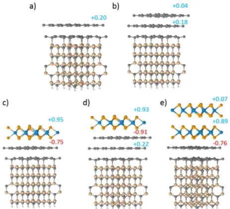
Figure 1 Atomic representation of the different unit cells used for the DFT calculations: (a) SLG/ZLG/SiC, (b) BLG/ZLG/SiC,
(c) WSe2/SLG/ZLG/SiC, (d) WSe2/BLG/SiC and (e) WSe2-180/WSe2/SLG/ZLG/SiC. In the last structure, the two WSe2 layers
present a mutual angle of 180o in order to avoid any particular symmetry aspect. NB: in this work, the graphene buffer layer is referred to as Zero Layer Graphene (ZLG). SLG: single (or mono-) layer graphene. BLG: bi-layer graphene. The calculated amounts of transferred charges are given for each atomic layer, positive or negative signs indicate an excess or a deficit of electrons, respectively.
of available 2D materials of different types and nature (metals, semiconductors and insulators) open fantastic perspectives for the exploration of novel 2D solid states physics [5]. This new fundamental research also paves the way toward novel low dimensional and high performance optoelectronic devices [6].
Among the multitude of potential vertical 2D heterostructures, coupling mono- or bi-layer graphene and transition metal dichalcogenides (TMDs) appears to be a promising approach to develop new optoelectronic systems, according to their complementary properties. As already well known, mono-layer graphene is an almost ideal semi-metal exhibiting extremely high carrier mobility and electrical conductivity thanks to the relativistic character of particles at the K-point of the reciprocal space [7]. On the other hand, group VI-B mono-layer transition metal dichalcogenides (TMDs) of the form MX2 (M = Mo, W ; X = S, Se, Te) are
direct bandgap semiconductors which exhibit exceptionally strong light matter interactions regarding to their thickness [8]. Several works have demonstrated that photo-induced interlayer charge and/or energy transfer [9,10] can occur at TMD interfaces. Various kinds of hybrid graphene-TMD photodetectors have been successfully realized, featuring ultrahigh gains [11], broad-band photo-responsivity
[12], fast photo-responsivities [13], and efficient near-infrared photo-detection [14]. We refer the reader to review articles [15] for a more comprehensive introduction to the field of hybrid graphene/TMD photo-detection. However, the interlayer charge/energy transfer processes remain the subject of intensive investigations [10,16].
In that frame, it remains crucial to improve our understanding of the band alignment and charge exchange in 2D TMD/graphene heterojunctions [17-22]. To address these questions, TMDs deposited on epitaxial graphene, itself grown on SiC(0001), constitute an excellent template. In the case of MoS2, it has notably been shown that the
graphene-TMDC interlayer interaction goes beyond a simple van der Waals interaction, in part due to charge transfer effects [23]. By using SiC(0001), one can easily obtain a surface featuring terraces with single-layer graphene (SLG) or bilayer graphene (BLG). This allows investigating at once the influence of the electronic properties of the substrate on the band offset and charge transfer mechanisms. In the case of WSe2/Gr and
WS2/Gr heterojunctions (HJs), scanning tunneling
spectroscopy [21] and angle resolved photoemission [22] measurements have in particular shown that the band offsets track the work function of the underlying single layer and bilayer graphene.
These observations point towards the absence of Fermi-level pinning in these HJs [24], which band alignment shall therefore follow the prediction of the Schottky-Mott model. A key ingredient of the Schottky-Mott model is that there should be no electrostatic discontinuity at the metal-semi-conductor (MS) interface (or equivalently that the vacuum level alignment is kept on both interface sides), since there are no interface states.
In the present work, we probe surface and interface electrostatics of tungsten diselenide (WSe2) layers deposited
by molecular beam epitaxy (MBE) on graphene mono-layers (SLG) and bi-layers (BLG), themselves grown on SiC(0001) substrates. Figure 1 provides an atomic representation of these interfaces. To carry out these investigations, we combine experimental Kelvin probe force microscopy (KPFM) measurements and Density Functional Theory (DFT) calculations, both techniques giving complementary access to the structural and electrical properties of the two-dimensional (2D) van der Waals heterojunctions (vHJ). KPFM is well suited to probe the band offsets at 2D HJs, charge transfer and/or interfacial dipoles. This technique yields a measurement of the vacuum-level variations at a sample surface, which are directly related to the energy band offsets [25] taking place at junctions between two different materials.
The KPFM surface potential images and the DFT calculations reveal the existence of an interface dipole resulting from an electron transfer from the graphene to the TMD. We show why this electrostatic discontinuity at the WSe2-Gr interface is not in contradiction with the prediction
of the Schottky-Mott model. In addition, we also observe a lateral band bending effect attributed to negatively charged defects at the TMD flakes edges, which amplitude is found to be consistent with the results of former STS reports [21].
2. Methods
Samples synthesis and processing
1-2 layer-thick graphene substrates were directly grown by chemical vapor deposition (CVD) on top of silicon-terminated face (0001) of n-doped (Nitrogen-doped) 6H-SiC. The CVD growth was performed by propane decomposition (C3H8) at
1550°C, under a mixed atmosphere of argon (Ar) and dihydrogen (H2) at 800 mbar (1 H2 for 10 Ar ratio). The CVD
growth under high partial pressure of Ar demonstrated high quality graphene formation [26]. It has been shown that a low H2/Ar ratio allows forming the so-called buffer layer in
between the SiC substrate and the graphene layer [27]. Increasing the H2/Ar ratio results in in-plane rotational
disorder, and to the formation of wrinkles [27].
All TMD monolayers (1L-TMD), namely tungsten diselenide (WSe2), were grown in van der Waals epitaxy [28]
on top of the 1-2 layer-thick graphene surface in a Molecular Beam Epitaxy (MBE) chamber, allowing the formation of
vertical 2D TMD/Gr van der Waals heterojunctions (vHJ). The MBE growths were performed with a base pressure of about 5.10−10 mbar which increased up to about 2.10−8 mbar
during the co-deposition of W and Se. The W and Se were respectively evaporated by an e-gun evaporator and a home-built evaporation cell. The Se pressure measured at the sample position with a retractable Bayard-Alpert gauge is about 1.10−6
mbar. The W deposition rate measured with a quartz balance monitor was 1.5 Å.min−1. The post-annealing was performed
at 720°C for 15 minutes under Se flux. A Se capping of about 100 nm is deposited after TMDs synthesis in order to prevent sample degradation during the air exposure from the MBE chamber to the AFM UHV-set-up. A medium-temperature annealing at 450°C is then performed for 1 hour under UHV in the preparation chamber of the VT-AFM to remove the Se-capping before nc-AFM/KPFM measurements.
nc-AFM/KPFM measurements
nc-AFM/KPFM experiments on graphene and WSe2/graphene were achieved under UHV conditions within
a beam deflection Omicron VT-AFM setup. Topographic imaging was performed in frequency modulation mode with frequency shifts (negative set-points for nc-AFM) and vibration amplitude of a few hertz and a few tens of nanometers, respectively. KPFM measurements were simultaneously acquired in frequency modulation mode (FM-KPFM) in single-pass mode. All data were obtained with super-sharp silicon cantilever (SuperSharpSilicon, Nanoworld, resonance frequency range: 250-320 kHz) annealed and ion sputtered under UHV in the preparation chamber of the VT-AFM to remove contaminants. The lateral resolution is estimated at 3-5 nm. The modulation bias Vac
(0.5 V peak-to-peak) and the KPFM compensation potential Vdc were applied to the cantilever (tip bias Vtip = Vdc), and the
Gr substrate was grounded. As Vdc is applied to the tip, the
contact potential difference (CPD) becomes equal to −Vdc. In
this work, the tip compensation bias (Vtip = −VCPD) was used
to represent the potentiometric data and was called for simplicity KPFM potential or surface potential.
Theoretical Calculations
Our calculations have been performed using the very efficient DFT localized orbital Fireball code [29]. Since the main features have been widely described elsewhere [30], we just mention here that this code uses a self-consistent version of the Harris−Foulke LDA functional [29,31] and that the self-consistency is achieved over the occupation numbers. Optimized numerical basis sets have been used for tungsten, selenium, carbon and silicon with respective cutoff radii in atomic units of s = 4.7, p = 5.2, d = 4.5 for W, s = 4.3, p = 4.8, d = 5.3 for Se, s = 4.5, p = 4.5 for C [32] and s = 4.8, p = 5.4 for Si.
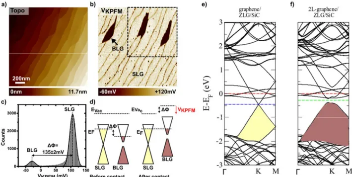
Figure 2 (a) Topographic nc-AFM image of the graphene substrate on 6H-SiC(0001). (b) KPFM image of the tip compensation
bias (Vtip =VKPFM, surface potential). (c) Histogram of the surface potential values recorded in the area delimited by dotted
contours in (b). (d) Schematic illustration of the band alignment of Single-layer Graphene (SLG) and Bi-Layer Graphene (BLG) before contact (thought experiment) and after contact. The lower surface potential pointed out over BLG areas can be interpreted as an upshift of the local vacuum energy level (Evac), regarding to the one of SLG, as depicted by the after contact band
alignment. The KPFM loop restores the vacuum level alignment by applying a compensation bias shifted in the opposite direction. At thermal equilibrium, the Fermi energy being equivalent for SLG and BLG, an upshift of Evac over BLG implies a
larger work function (ΔΦ ≈ 135±2 meV). (e,f) DFT calculated bandstructures of graphene on ZLG/SiC (e) and bilayer graphene on ZLG/SiC (f). The dashed red, blue and green lines show respectively the Fermi level, the position of the Dirac cone of the monolayer graphene and the mid-gap of the bilayer graphene. All the energies are referred to the Fermi level
The Fireball code has been used to optimize the different structures considered in this work, namely, a 3 × 3 unit cell of graphene buffer layer (or Zero Layer Graphene, ZLG) on top of a five layer SiC slab, with either one or two graphene layer on top (as reference systems), and one or two WSe2 layer on
top of all. These different systems, represented in Figure 1, have been optimized until the forces were below 0.1 eV/Å. Since vdW interaction is not properly described in DFT, we have considered an extra perturbation theory method, the LCAO-S2 + vdW approach [33], to accurately determine the interlayer equilibrium configuration. This approach is based on the dipolar approximation for vdW interaction and has already been used successfully in graphitic and 2D materials, in good agreement with experimental determinations [23,34,35].
Once the equilibrium configuration is found, the electronic structure of each system has been analyzed by means of band structure and charge transfer calculations. A set of 300 specific k-points along the Γ−K−M path has been used for band structure calculations.
3. Results and discussion
At first, it is mandatory to characterize finely the CVD grown graphene substrate on SiC, since it forms template for the TMD growth. Figure 2 displays topographic and potentiometric nc-AFM/KPFM images recorded on the graphene substrate after in situ (i.e. under UHV) annealing at ca. 720°C (same temperature that the one used for the WSe2
growth process). The topographic image shown in Figure 2(a) features several hundred nanometers wide parallel terraces. The step height deduced from height profiles (not shown) is mainly of 7.5 ± 0.3 Å (three interatomic Si-C distance each of 2.5 Å), as expected for the surface morphology of few-layer graphene grown on 6H-SiC (0001) substrates. In addition, no height differences can be measured within terraces, indicating the growth of a continuous graphene layer with a homogeneous thickness over entire terraces. In particular, the absence of wrinkles, generally characteristic of in-plane rotational disorder [36], suggests a monocrystalline character over several microns (scale of the nc-AFM images) or at least on a given terrace.
Figure 2(b) displays the surface potential image (KPFM tip compensation bias) acquired simultaneously with the
Figure 3 (a) Topographic nc-AFM image of the system after growth of WSe2 flakes on top of the graphene substrate. (b) KPFM
image of the tip compensation bias (Vtip =VKPFM, surface potential). The arrow pinpoints a BLG area. (c) Histogram of the
surface potential values recorded in the area delimited by dotted contours in (b). topographic image. This surface potential map permits to
identify regions with two distinct contrast levels: a homogeneous surface potential level observed over the majority of the sample and darker patches, displaying a lower surface potential compared to the main level. Consistently with the results of the literature [37] and with complementary characterization performed by scanning electron microscopy (SEM) co-localized with Raman spectroscopy mapping (see Figure S1 in the supplementary information), the main level can be attributed to single-layer graphene (SLG), while dark patches corresponds to bilayer graphene (BLG) regions.
This relies on the fact that the graphene doping by the substrate decreases with the graphene thickness. In the case of graphene grown on SiC(0001), it is well known that the first graphene layer is n-doped by by the buffer layer with a (6√3 6√3)R30° periodicity between the graphene and the SiC [38,39]. Due to the electrostatic screening by the first layer, the second layer is less n-doped, resulting in a larger work function in case of BLG regarding to the SLG work function. The resulting band alignment is depicted in Figure 2(d), which shows the electron-doped Dirac cones for SLG and BLG (less n-doped and with a gap opening, as discussed hereafter) before and after contact at thermal equilibrium. Due to the BLG higher work function, the local vacuum level is shifted upward over the BLG. This shift is compensated by applying a more negative compensation bias on the AFM tip, accounting for the observed contrasts.
This situation is in overall well reproduced by the DFT calculations for mono- and bi-layer graphene on ZLG/SiC (here ZLG stands for Zero Layer Graphene, a 3 × 3 unit cell of graphene buffer layer, see Methods). In Figure 2 (e) and (f) we represent the band-structure calculations on these two systems note that all the energies are referred to the Fermi level). In Fig. 2(e), we can observe the graphene n-doping
induced by the buffer/SiC substrate with a Dirac point located at 450 meV below the Fermi level. Fig. 2(f) shows a gap opening of ~160 meV in the graphene bilayer, due to the symmetry breaking induced by the charge transfer with the substrate. Hence, the lower graphene layer in the bilayer is doped by the ZLG/SiC substrate and presents a different charge density with respect to the upper graphene layer. As a consequence, an electric field is generated between the layers, which breaks the symmetry and opens a gap in the structure [23,34]. From the DFT calculations, we can extract the electronic charge transfers of each layer in the unit cell. The lower graphene layer gains 0.18 electrons per unit cell, coming from the ZLG/SiC substrate, whereas the upper graphene layer gains only 0.04 electrons coming from the lower graphene layer (see Figure 1(b)).
The KPFM surface potential variation between SLG and BLG (see the histogram in Figure2 (c)), permits to estimate a work function difference of 135 ±2 mV, in excellent qualitative agreement with previous studies performed on few-layers graphene grown on 6H-SiC (0001)[37,40-45]. As a matter of comparison, the Fermi level calculated for the SLG/ZLG/SiC system is shifted above the one of the BLG/ZLG/SiC by +102mV. This slight underestimation may originate from the intrinsic defects of DFT which does not properly take into account the excitations in a system, leading to an underestimation of the gap. In the present case, the gap underestimation is also related to a slight underestimation of the Fermi level position.
We turn now to the structural and electronic properties of the WSe2/Graphene heterojunction (HJ). The growth
conditions were chosen in order to get a sub-monolayer TMD coverage and keep uncovered graphene regions, so as to reference the KPFM surface potential and to be able to discriminate between SLG and BLG. Figures 3(a,b) shows the nc-AFM topography and the associated surface potential (SP)
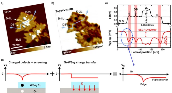
Figure 4 (a,b) Topographic nc-AFM image (a) and surface potential image (b) of two WSe2 islands located over SLG
(255255nm). D-1L, D-2L and DB arrows pinpoint structural (and charged) defects in the first (D-1L) and second (D-2L) WSe2 layers, and a domain (or twin) boundary (DB). (c) Topographic and potentiometric cross-section profiles corresponding
to the paths in (a) and (b). The vertical arrows highlight local topographic sur-elevations at the step edge and over the domain boundary. Half-transparent red bars (guideline for the eye only) indicate approximately the position of band-bending regions.
(d) Schematic representation of the contributions to the surface potential of charged defects at the step edges and of the effective
interface dipole (D) resulting from electron transfer from the graphene to the WSe2. The black and white dots represent a
negatively charged defect at the WSe2 edge and an effective counter charge of opposite sign due to electrostatic screening by
the graphene substrate.
of a representative area of the WSe2/Gr sample. From the
topographic image, substrate terraces delimited by step edges can still be observed. The images clearly reveal the growth of WSe2 flakes covering approximately 30% of the surface (this
surface coverage value has been obtained by analyzing the distribution of the SP levels, see Figure S2 in the supplementary information). Thanks to the reference measurements carried out on the bare substrate (Figure 2), distinct areas can be unambiguously associated with SLG or BLG (the location of a BLG patch is highlighted by an arrow in Figure 3(b)). Both KPFM measurements (i.e. on the bare substrate and on the WSe2/Graphene sample) yield the same
work function difference between SLG and BLG within the error bar (compare the SP histograms in Figure 2(c) and in Figure 3(c)).
Whether we are considering SLG or BLG areas, the surface potential measured over the WSe2/Gr heterojunctions is in
average lower by several hundreds of mV than the one measured over the bare graphene layer. This effect can be understood in two ways: (i) the lower SP measured over HJ indicates a larger WF (ii) the SP variation can be interpreted by the presence of an effective out-of-plane surface dipole
pointing downward, resulting from an interfacial charge transfer between the WSe2 flakes and the graphene substrate.
The downward orientation of the surface dipole indicates that electrons have been transferred from the underlying graphene to the WSe2 flakes.
Further insight on the nanoscale morphology and electronic properties can be gained by recording images at smaller scales. Figure 4a presents a 3D plot of the surface topography of two WSe2 islands, grown at the vicinity and over a graphene step.
In Figure 4b, the same topographic levels are combined with the KPFM potential information (used for the color code) in a unique 3D plot. This mixed representation facilitates the identification of correlations between the topographic and potentiometric contrasts.
These images reveal that the WSe2 domains consist in
mono-layer (1L) islands partially covered by a second layer (2L), with stacking heights of ca. 0.68nm (see the topographic profile in Figure 4c). These values are close to the ones reported by others for MBE-grown WSe2 on graphite [46]. In addition, the topographic image reveals the existence of defects, which appear in the form local sur-elevations (typ. 0.3nm) with regard to the expected stacking heights for the first and second layers. In Figure 4a, two arrows labelled
D-1L and D-2L pinpoint the location of some of these defects in the first (D-1L) and second (D-2L) WSe2 layers (additional
topographic profiles crossing these corrugations are provided in the supplementary information, see Figure S3).
A closer examination reveals the existence of other kinds of defects. First, one can see that the domain edge is slightly sur-elevated in most of its parts with respect to the flake interior. It is thus likely that the edges are in part decorated with another material such as Se clusters or residual molecules (such as hydrocarbons, O2, H2O), which has already been
observed for MBE-grown samples [46-48]. Similar sur-elevations forming inversion domain boundaries (DB) are also present inside the WSe2 flake (one DB is highlighted by an
arrow in Figure 4). The existence of such domain (or twin) boundaries is also not surprising; others [23] have already mentioned their existence for TMD layers grown by molecular beam epitaxy [49].
Obviously, the flakes are not homogeneously charged, and the nanostructure has a deep impact on the electrostatic landscape. First, one observes an important edge effect. The WSe2 islands are indeed clearly surrounded by dark halos in
the surface potential images (Figure 4(b)). In other words, the surface potential falls down at the edge of the 1L-WSe2 flake,
i.e. goes to more negative values with respect to the ones measured above the monolayer interior. A simple argument rules out the possibility of an artefact induced by tip convolution/averaging at the flake’s edge: in such a scenario, we would expect the surface potential to take a value comprised between the ones measured above adjacent materials (i.e. between the interior of the 1L-WSe2 flake and
SLG surface), which is not the case here. We also note that the surface potential reaches its lowest (i.e. more negative) level over the local structural defects that correspond to the highest deviations with respect to the expected height values for the first and second TMD layers (D-1L and D-2L); in other words these defects are negatively charged, too. However, the exact nature of these defects remains uncertain; we will thus restrict the discussion to the case of flake edges (and domain boundaries) in the following.
In first analysis, the observation of “dark SP halos” at the flake edges is in good agreement with the results of scanning tunneling spectroscopy measurements (STS) reported by LeQuang et al. for similar samples [48]. Their STS experiments pointed out a significant lateral (in the 1L-TMD plan) band bending occurring in the vicinity of WSe2/vacuum
interfaces. This effect was explained by assuming the existence of n-type-like charged defects at the flake edges, which electrostatic field is screened out by the free carriers in the graphene layer (as depicted in Figure 4d).
The presence of such negatively charged sites is consistent with the lower surface potential observed at the edge of the flakes, as well as over the domain boundaries. A band-bending of ca. 300mV (over 5nm) was extracted from the STS data
[48] on 1L-WSe2, which is close to the values deduced from
the KPFM surface potential profiles (see the potentiometric profiles in Figure4c and in Figure S3). In our case, however, the lateral extension of the band bending region (of the order of a few nanometers) could not be accurately measured, due to convolution effects with the AFM tip (the impact of these effects on the topographic and potentiometric profiles is illustrated in Figure S3).
The band-bending value is obtained by comparing the surface potential levels measured at the edge and at the interior (over the first WSe2 layer) of the flake. Here, it is crucial to
note that the surface potential at the interior of the flake (out of the band bending region) is lower by ca. 300mV than the one measured over the SLG. This confirms that the WSe2
islands are intrinsically negatively charged, or (equivalently) that an interface dipole oriented downward exist at the WSe2/graphene interface. It means that the negative charging
of WSe2 domains does not solely originate from charged
defects at the edges. The vertical interface dipole and the lateral band bending contribute simultaneously to the global electrostatic landscape probed by KPFM, as depicted in Figure 4d.
On a theoretical point of view, DFT calculations confirm the existence of an important electron transfer from the monolayer graphene to the WSe2 monolayer. In Figure 5 (left
and middle pannels), we compare the DFT calculated band-structures of SLG (SiC/ZLG/graphene) and of 1L-WSe2 on
SLG (SiC/ZLG/graphene/ WSe2). In addition, the charges per
unit cell resulting from the interfacial charge transfers are given in Figure 1. The WSe2 layer gains 0.95 electrons per unit
cell from the monolayer graphene, which loses 0.75 electrons (per unit cell). Thus, the charge transfer cancels the n-doping from the ZLG/SiC substrate, as it can be seen from Fig. 5 with the relocation of the Dirac point closer to the Fermi level. Consequently, we can state that the TMD monolayer neutralizes the extra charge given to graphene by the ZLG/SiC substrate. We can interpret this charge transfer as an electrostatic reaction of the system to the initial non-equilibrium state of the graphene doped by the substrate. In that respect, the TMD is less perturbed by the gained electronic charges, due to its semiconducting nature, which allows absorbing a small electronic density in the gap, which is not the case of graphene of semi-metallic nature.
These joint experimental and theoretical evidences of a negative charge transfer from the graphene substrate to the TMD invite us to reconsider the band alignment model for WSe2/Gr-SiC interface. Several theoretical and experimental
works have already shown that graphene-TMD interfaces display very weak Fermi level pinning thanks to the absence of metal-induced gap states (MIGS) [21,24]. The conclusions of these studies are all in line with the Schottky-Mott model, which predicts that in the absence of interface states, the energy difference between the semiconductor’s conduction
Figure 5 From left to right, DFT calculated band-structures of SLG (SiC/ZLG/graphene), 1L-WSe2 on SLG
(SiC/ZLG/graphene/ WSe2) and of 2L-WSe2 on SLG (SiC/ZLG/graphene/WSe2-WSe2 180). The dashed red and blue lines
show respectively the Fermi level and the position of the Dirac cone of the monolayer graphene.
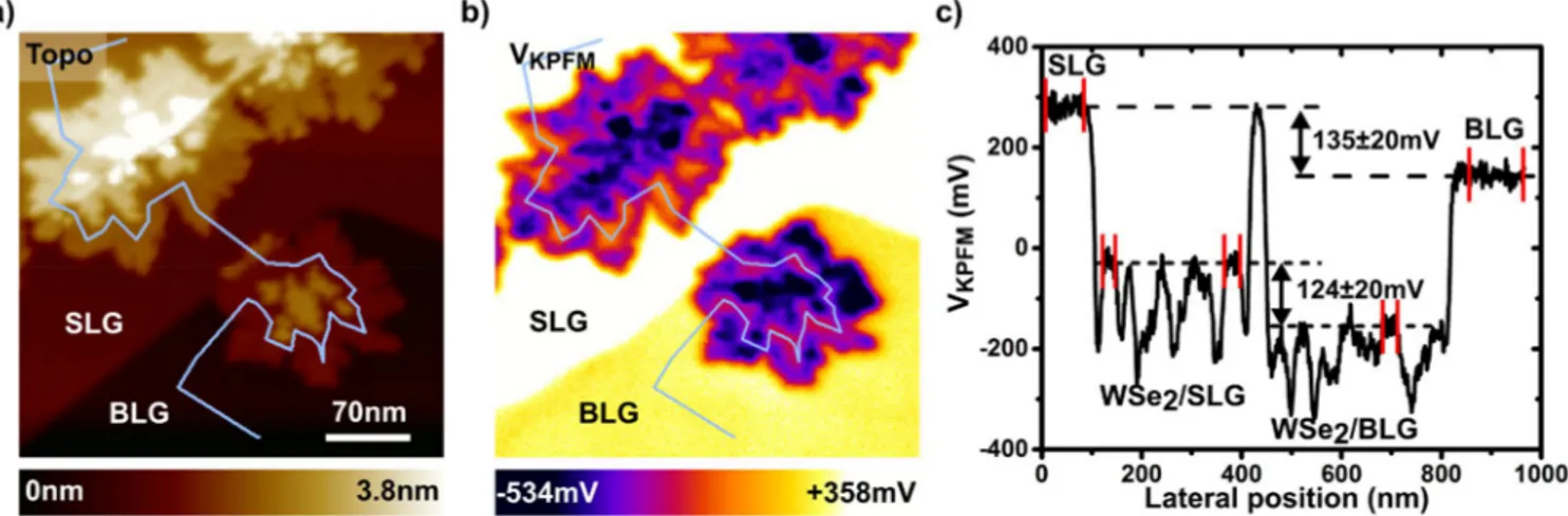
Figure 6 (a,b) Topographic nc-AFM image (a) and surface potential image (b) of two WSe2 islands grown on both sides of an
SLG-BLG border (351351nm). (c) Potentiometric cross-section profile corresponding to the paths in (a) and (b). Red bars indicate the lateral positions in between which average values of the SP have been calculated. The SP shift between WSe2/SLG
and WSe2/BLG has been calculated by considering the areas displaying the highest (in average) SP values. The error bars have
been estimated from standard deviation values.
band minimum and the metal work function at the interface (i.e. the Schottky barrier, SBH) shall be equal to the difference between the metal work function (M) and the semiconductor
electron affinity (). As abovementioned, the Schottky-Mott model implies that there is no electrostatic discontinuity at the metal-semi-conductor (MS) interface, since there are no
interface states. However, we note that in its classical form (i.e. in the case of an interface between three-dimensional materials), this model does not exclude the existence of an effective interface dipole resulting from the charge transfer (necessary to Fermi level alignment) across the MS interface. This charge transfer results in a band bending on the
semiconductor side that goes with an equivalent shift of the vacuum level (this situation is illustrated in the literature[50]). In our case, there is no more space charge or band-bending region in the vertical direction due to the two dimensional nature of the stacked materials. The DFT calculations and KPFM data demonstrate nonetheless the existence of an interface dipole originating from electron transfer on both sides of the WSe2/Gr interface. Representing at once this
dipole (with the vacuum level shift linked to it) and the energy bands in a Schottky-Mott configuration (fulfilling a vacuum alignment condition) is conceptually difficult (see Figure S4 in the supplementary information); this brings once again to light the exceptional nature of two-dimensional TMD/graphene interfaces.
Comparing the interface dipoles for WSe2/SGL and
WSe2/BLG provides another way to approach the problem. As
pointed out by LeQuang et al. [21], the validity of the Schottky-Mott rule (i.e. a linear dependence of the Schottky barrier as a function of the metal work function) is preserved only if the interface dipole is identical for both systems. Such a comparison is presented in Figure 6, which displays nc-AFM/KPFM data recorded over two WSe2 domains grown on
both sides of a step edge delimiting BLG – SLG areas. The overall contrast of the surface potential map (Figure 6b) reveals clearly that the vacuum level variations over the WSe2
flake follow the substrate ones. A quantitative analysis can be performed by drawing a cross section profile that matches approximately the flake interior on both sides of the SLG-BLG border; this analysis (Figure 6c) confirms that the vacuum level shift follows rigidly the one of the substrate within the measurement error bar. DFT calculations confirm that the charge transfer is almost identical across WSe2/SLG
and WSe2/BLG interfaces, with an excess of 0.95 electrons
>and 0.93 electrons per unit cell for the TMD layer (Figure 1), respectively. Overall, these results confirm that the band alignment and charge transfer for the WSe2/Gr system can be
effectively accounted in the frame of the Schottky-Mott model.
To complete this study on the charge transfer, we finally consider the case of the second TMD layer. The DFT calculations (Figure 5) indicate that the first TMD layer absorbs almost all the excess charges contained in the graphene. Figure 1(e) presents the atomic configuration for two WSe2 layers on SLG/ZLG/SiC, rotated by 180 degrees
one with respect to the other (this configuration was chosen in order to avoid any symmetry consideration, since no specific angle between the layers can be deduced from the experimental data). One observes no significant difference between the different band-structures calculated with one or two WSe2 monolayer (Figure 5). The charge transfer analysis
(as represented in Figure 1(e)) reveals that the lower and upper WSe2 layers gain +0.89 and +0.07 electron per unit cell,
respectively.
This last result indicates that the second WSe2 layer (2L) is
unlikely to play a significant role in the electrostatics of the system. Nevertheless, compared to the interior of the first WSe2 layer (1L), the surface potential is in average lower by
300mV over the second layer islands, as shown by the cross-section profile in Figure 4(c) (note that the structural defects displaying an improper stacking height have been excluded from this analysis). This apparent contradiction can be resolved by assuming that similarly to the case of 1L-WSe2,
n-type-like charged defects exist at 2L-WSe2 edges. This
hypothesis is also supported by the fact that the SP decrease over 2L domains is almost equal to the one observed over 1L edges. The absence of well-marked halos in the SP image at the periphery of 2L domains can be for its part understood by taking into account the reduced dimension of the 2L domains and convolution effects, which prevent an accurate visualization of the band bending region extension. Further investigations on samples displaying larger bilayer domains would be needed to definitely confirm that the slight negative charge excess calculated by DFT has a negligible impact on the electrostatic potential probed by KPFM.
4. Conclusion
In summary, we have investigated the electronic properties of MBE-grown WSe2 layers on graphene (single-layer and
bilayer graphene on SiC(0001)) by Kelvin Probe Force Microscopy and Density Functional Theory (DFT) calculations. Overall, our results show that the global electrostatic landscape probed by KPFM originates from the joint contributions of charged defects and charge transfers at the TMD-substrate interface. Charged defects at the flake edges affect the electrostatic landscape probed by KPFM, by inducing a lateral band bending which value is fully consistent with the results of former investigations by scanning tunneling spectroscopy. The initial n-doping of the graphene monolayer on SiC is neutralized by the adsorption of the TMD, resulting in the existence of an interface dipole at the TMD/graphene interface. The vacuum level shift induced by this charge transfer is identical within the experimental error over single-layer and bisingle-layer graphene, which confirms that these interfaces can be described in a 2D version of the Schottky-Mott model where the spatially extended band bending area in the vertical direction on the semiconductor side is replaced by an interface dipole.
Acknowledgments
Financial support by the Agence Nationale de la Recherche (France) with the 2DJ project (ANR-15-CE24-0017) is gratefully acknowledged.
Benjamin Grévin https://orcid.org/0000-0002-6494-8138
References
[1] Hellerstedt J, Yudhistira I, Edmonds M T, Liu C, Collins J, Adam S and Fuhrer M S 2017 Electrostatic Modulation of the Electronic Properties of Dirac Semimetal Na3Bi Thin
Films Phys. Rev. Materials 1 054203
[2] Rocha M A A, Coutinho J A P and Santos L M N B F 2013 Evidence of Nanostructuration from the Heat Capacities of the 1,3-dialkylimidazolium bis(trifluoromethylsulfonyl)imide Ionic Liquid Series J. Chem. Phys. 139 104502
[3] Weiner P K, Langridge R, Blaney J M, Schaefer R and Kollman P A 1982 Electrostatic Potential Molecular Surfaces PNAS 79 3754-8
[4] Chau R, Datta S, Doczy M, Doyle B, Jin B, Kavalieros J, Majumdar A, Metz M and Radosavljevic M 2005 Benchmarking Nanotechnology for High-Performance and Low-Power Logic Transistor Applications 2005 IEEE Transactions on Nanotechnology 4 153-8
[5] Novoselov K S, Mishchenko A, Carvalho A and Castro Neto A H 2016 2D materials and van der Waals heterostructures Science 353, aac9439
[6] Shim J, Kang D H, Kim Y, Kum H, Kong W, Bae S H, Almansouri I, Lee K, Park J H and Kim J 2018 Recent Progress in van der Waals (vdW) Heterojunction-Based Electronic and Optoelectronic Devices Carbon 133 78-89 [7] Castro Neto A H, Guinea F, Peres N M R, Novoselov K S and Geim A K 2009 The Electronic Properties of Graphene Rev. Mod. Phys. 81 109-62
[8] Britnell L, Ribeiro R M, Eckmann A, Jalil R, Belle B D, Mishchenko A, Kim Y-J, Gorbachev R V, Georgiou T, Morozov S V, Grigorenko A N, Geim A K, Casiraghi C, Castro Neto A H and Novoselov K S 2013 Strong Light-Matter Interactions in Heterostructures of Atomically Thin Films Science 340 1311-4
[9] Shim G W, Yoo K, Seo S B, Shin J, Jung D Y, Kang I S, Ahn C W, Cho B J and Choi S Y 2014 Large-Area Single-Layer MoSe2 and Its van der Waals Heterostructures ACS Nano 8 6655–62
[10] Froehlicher G, Lorchat E and Berciaud S 2018 Charge Versus Energy Transfer in Atomically Thin Graphene-Transition Metal Dichalcogenide van der Waals Heterostructures Phys Rev X 8 011007
[11] Zhang W, Chuu C P, Huang J K, Chen C H, Tsai M-L, Chang Y-H, Liang C-T, Chen Y-Z, Chueh Y-L, He J-H, Chou M-Y and Lib L-J 2014 Ultrahigh-Gain Photodetectors Based on Atomically Thin Graphene-MoS2 Heterostructures. Sci
Rep. 4 3826
[12] Mudd G W, Svatek S A, Hague L, Makarovsky O, Kudrynskyi Z R, Mellor C J, Beton P H, Eaves L,Novoselov K S, Kovalyuk Z D, et al. High Broad-Band Photoresponsivity of Mechanically Formed InSe–Graphene van der Waals Heterostructures 2015 Adv. Mater. 27 3760–3766
[13] Massicotte M, Schmidt P, Vialla F, Schädler K G, Reserbat-Plantey A, Watanabe K, Taniguchi T, Tielrooij K J and Koppens F H L 2016 Picosecond Photoresponse in van der Waals Heterostructures Nature Nanotechnology 11 42–6 [14] Yu W, Li S, Zhang Y, Ma W, Sun T, Yuan J, Fu K and Bao Q 2017 Near-Infrared Photodetectors Based on MoTe2/Graphene Heterostructure with High Responsivity and Flexibility Small 13 1700268
[15] Geng H, Yuan D, Yang Z, Tang Z, Zhang X, Yang K, Su Y Graphene van der Waals Heterostructures for High-Performance Photodetectors 2019 J. Mater. Chem. C 7 11056 [16] Yuan L, Chung T-F, Kuc A, Wan Y, Xu Y, Chen Y P, Heine T and Huang L 2018 Photocarrier Generation from Interlayer Charge-Transfer Transitions in WS2-Graphene
Heterostructures Sci. Adv. 4 e1700324
[17] Larentis S, Tolsma J R, Fallahazad B, Dillen D C, Kim K, MacDonald A H and Tutuc E 2014 Band Offset and Negative Compressibility in Graphene-MoS2 Heterostructures
Nano Lett. 14 2039–45
[18] Kim K, Larentis S, Fallahazad B, Lee K, Xue J, Dillen D C, Corbet C M and Tutuc E 2015 Band Alignment in WSe2–
Graphene Heterostructures ACS Nano 9 4527–32
[19] Jin C, Rasmussen F A and Thygesen K S 2015 Tuning the Schottky Barrier at the Graphene/MoS2 Interface by
Electron Doping: Density Functional Theory and Many-Body Calculations J. Phys. Chem. C 119 19928–33
[20] Pierucci D, Henck H, Avila J, Balan A, Naylor C H, Patriarche G, Dappe Y J, Silly M G, Sirotti F, Johnson A T C, Asensio M C and Ouerghi A 2016 Band Alignment and Minigaps in Monolayer MoS2-Graphene van der Waals
Heterostructures Nano Lett. 16 4054–61
[21] Le Quang T, Cherkez V, Nogajewski K, Potemski M, Dau M T, Jamet M, Mallet P and Veuillen J-Y 2017 Scanning Tunneling Spectroscopy of van Der Waal Graphene/Semiconductor Interfaces: Absence of Fermi Level Pinning 2D Mater 4 035019.
[22] Ulstrup S, Giusca C E, Miwa J A, Sanders C E, Browning A, Dudin P, Cacho C, Kazakova O, Myers-Ward R L, Zhang T, Terrones M and Hofmann P 2019 Nanoscale mapping of quasiparticle band Alignment Nat. Commun. 10 3283 [23] Dau M T, Gay M, Di Felice D, Vergnaud C, Marty A, Beigné C, Renaud G, Renault O, Mallet P, Le Quang T, Veuillen J-Y, Huder L, Renard V T, Chapelier C, Zamborlini G, Jugovac M, Feyer V, Dappe Y J, Pochet P and Jamet M 2018 Beyond van Der Waals Interaction: The Case of MoSe2 Epitaxially Grown on Few-Layer Graphene ACS Nano 12 2319–31
[24] Liu Y, Stradins P and Wei S-H 2016 Van der Waals metal-semiconductor junction: Weak Fermi level pinning enables effective tuning of Schottky barrier Sci. Adv. 2 e1600069
[25] Cahen D and Kahn A 2003 Electron Energetics at Surfaces and Interfaces: Concepts and Experiments Adv. Mater. 15 271– 77
[26] Portail M, Michon A, Vézian S, Lefebvre D, Chenot S, Roudon E, Zielinski M, Chassagne T, Tiberj A, Camassel J and Cordier Y 2012 Growth Mode and Electric Properties of Graphene and Graphitic Phase Grown by Argon–Propane Assisted CVD on 3C–SiC/Si and 6H–SiC J. Cryst. Growth
349 27–35
[27] Michon A, Largeau L, Tiberj A, Huntzinger J-R, Mauguin O, Vézian S, Lefebvre D, Cheynis F, Leroy F, Müller P, Chassagne T, Zielinski M and Portail M 2013X-ray Diffraction and Raman Spectroscopy Study of Strain in Graphene Films Grown on 6H-SiC(0001) Using Propane-Hydrogen-Argon CVD Materials Science Forum 740-742 117-120
[28] Walsh L A and Hinkle C L 2017 van der Waals Epitaxy: 2D Materials and Topological Insulators Applied Materials Today 9 504-515
[29] Harris J 1985 Simplified Method for Calculating the Energy of Weakly Interacting Fragments Phys. Rev. B 31 1770−9
[30] Jelínek P, Wang H, Lewis J P, Sankey O F and Ortega J 2005 Multicenter Approach to the Exchange-Correlation Interactions in Ab Initio Tight-Binding Methods Phys. Rev. B
71 235101
[31] Foulkes W M C and Haydock R 1989 Tight-Binding Models and Density-Functional Theory Phys. Rev. B 39 12520−36
[32] Basanta M, Dappe Y J, Jelinek P and Ortega J 2007 Optimized Atomic-Like Orbitals for First-Principles Tight-Binding Molecular Dynamics J. Comput. Mater. Sci. 39 759−66
[33] Dappe Y J, Ortega J and Flores F 2009 Intermolecular Interaction in Density Functional Theory: Application to Carbon Nanotubes and Fullerenes Phys. Rev. B 79 165409 [34] Pierucci D, Sediri H, Hajlaoui M, Velez-Fort E, Dappe Y J, Silly M G, Belkhou R, Shukla A, Sirotti F, Gogneau N and Ouerghi A 2015 Self-Organized Metal-Semiconductor Epitaxial Graphene Layer on Off-Axis 4H-SiC(0001) Nano Research 8 1026-37
[35] Dappe Y J and Martinez J I 2013 Effect of van der Waals Forces on the Stacking of Coronenes Encapsulated in a Single-Wall Carbon Nanotube and Many-Body Excitation Spectrum Carbon 54 113-23
[36] Michon A, Vézian S, Ouerghi A, Zielinski M, Chassagne T and Portail M 2010 Direct Growth of Few-Layer Graphene on 6H-SiC and 3C-SiC/Si via Propane Chemical Vapor Deposition Appl. Phys. Lett. 97 171909
[37] Filleter T, Emtsev K V, Seyller T and Bennewitz R 2008 Local Work Function Measurements of Epitaxial Graphene Appl. Phys. Lett. 93 133117
[38] Ristein J, Mammadov S and Seyller T 2012 Origin of Doping in Quasi-Free-Standing Graphene on Silicon Carbide. Phys.Rev. Lett. 108 246104
[39] Miwa J A, Dendzik M, Grønborg S S, Bianchi M, Lauritsen J V, Hofmann P and Ulstrup S Van der Waals Epitaxy of Two-Dimensional MoS2-Graphene
Heterostructures in Ultrahigh Vacuum 2015 ACS Nano 9 6502–6510
[40] Lee N J, Yoo J W, Choi Y J, Kang C J, Jeon D Y, Kim D C, Seo S and Chung H J 2009 The Interlayer Screening Effect of Graphene Sheets Investigated by Kelvin Probe Force Microscopy Appl. Phys. Lett. 95 222107
[41] Hibino H, Kageshima H, Kotsugi M, Maeda F, Guo F-Z and Watanabe Y 2009 Dependence of Electronic Properties of Epitaxial Few-Layer Graphene on the Number of Layers Investigated by Photoelectron Emission Microscopy Phys. Rev. B 79 125437
[42] Ziegler D, Gava P, Güttinger J, Molitor F, Wirtz L, Lazzeri M, Saitta A M, Stemmer A, Mauri F and Stampfer C 2011Variations in the Work Function of Doped Single- and Few-Layer Graphene Assessed by Kelvin Probe Force Microscopy and Density Functional Theory Phys. Rev. B 83 235434
[43] Panchal V, Pearce R, Yakimova R, Tzalenchuk A and Kazakova O 2013 Standardization of Surface Potential Measurements of Graphene Domains Sci. Rep. 3 2597 [44] Melios C, Spencer S, Shard A, Strupiński W, Silva S R P and Kazakova O 2016 Surface and Interface Structure of Quasi-Free Standing Graphene on SiC 2D Mater. 3 025023 [45] Leenaerts O, Partoens B, Peeters F M, Volodin A and Van Haesendonck C 2017 The Work Function of Few-Layer Graphene J. Phys. Condens. Matter 29 035003
[46] Park J H, Vishwanath S, Liu X, Zhou H, Eichfeld S M, Fullerton-Shirey S K, Robinson J A, Feenstra R M, Furdyna J, Jena D, Xing H G and Kummel A C 2016 Scanning Tunneling Microscopy and Spectroscopy of Air Exposure Effects on Molecular Beam Epitaxy Grown WSe2 Monolayers
and Bilayers ACS Nano 10 4258-67
[47] Zhang C, Johnson A, Hsu C-L, Li L-J and Shih C-K 2014 Direct Imaging of Band Profile in Single Layer MoS2 on Graphite: Quasiparticle Energy Gap, Metallic Edge States, and Edge Band Bending Nano Lett. 14 2443–7
[48] Le Quang T, Nogajewski K, Potemski M, Dau M T, Jamet M, Mallet P and Veuillen J-Y 2018 Band-Bending Induced by Charged Defects and Edges of Atomically Thin Transition Metal Dichalcogenide Films 2D Mater. 5 035034 [49] Alvarez C J, Dau M T, Marty A, Vergnaud C, Le Poche H, Pochet P, Jamet M and Okuno H 2018 Impact of a van der Waals interface on intrinsic and extrinsic defects in an MoSe2 monolayer Nanotechnology 29 425706
[50] Vilan A and Cahen D 2017 Chemical Modification of Semiconductor Surfaces for Molecular Electronics Chem. Rev. 117 4624−66
Supporting Information
Graphene characterization by co-localized SEM imaging and
µ-Raman mapping
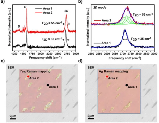
Figure S1. (a) Raman spectra (corrected from the contributions of the raw SiC substrate) extracted from two different areas of the graphene substrate. The Raman intensity is normalized to the 2D-band. (b) Raman 2D-bands. The full width at half maximum (FWHM) of the 2D contribution (Γ2D) estimated
at 35cm-1 in the area 1 and the good fitting performed thanks to a unique Lorentzian contribution
indicate that area 1 is cover by a Single-Layer Graphene (SLG) substrate. On the other hand, Γ2D in the
area 2 is measured around 55 cm-1 and 4 Lorentzian contributions are needed to ensure a satisfying
data adjustment, in agreement with the presence of Bi-Layer Graphene (BLG) in an AB-stacking order. (c,d) Co-localized SEM image and µ-Raman mapping. (c) Superposition of SEM image and Raman map of the 2D-band FWHM. Bright areas in the Raman map corresponds to higher Γ2D values characteristic
and bright areas in the Raman map (Area 2). (d) Superposition of SEM image and Raman map representing the integrated area of the G-band (AG). Bright areas corresponds to higher AG values. As
AG is known to increase with the number of graphene layers, the AG Raman map confirms the Bi-Layer
character of areas 2.
Raman measurements were performed using a confocal Renishaw InVia Raman
micro-spectrometer using a 532 nm laser excitation source with an average power of 0.7 µW focused
on a ~ 0.5 µm beam diameter. The top view SEM images were carried out with a scanning
electron microscope (Zeiss FE-SEM Ultra) operating at 1.5 kV. Raman and SEM images are
co-localized. Two marks were drawn on the sample with a diamond tip enabling the repositioning
when using different characterization equipments.
Figure
S1
presents the results of the (graphene) substrate characterization by co-localized
scanning electron microscopy (SEM) and micro-Raman (µ-Raman) spectroscopy imaging.
Raman spectra and co-localized images obtained by superposing SEM images and Raman
µ-maps are shown in the upper panels and lower panels, respectively.
SEM images (Figure
S1(c,d)
) feature dark patches covering approximately 5% of the surface
(Area 2), while the rest of the sample’s surface is mainly dominated by a brighter uniform
contrast (Area 1). In addition bright strips, separated by several hundred of nanometer, can
be observed and associated to SiC step edges. According to its sensitivity to work function
differences [
1-3
], secondary electron contrasts reveal the presence of regions with different
work functions, due to various numbers of graphene sheets, as demonstrated hereafter.
In order to ascertain the graphene thickness and get further information on its properties
[
4
], co-localized Raman spectroscopy and mapping has been performed. In Figure
S1(c)
, a
hyperspectral mapping of the Full Width at Half Maximum (FWHM) of the graphene 2D band,
named Γ
2Din the following, is superimposed to the SEM image. The main information is that
brighter regions, which represent higher values of Γ
2D, show a one-by-one correspondence
with dark SEM regions (Areas 2).
Figure
S1(a)
presents two finely located Raman spectra, respectively extracted from area 1
(black dot) and area 2 (red diamond). Note that the Raman contributions of the raw SiC
substrate have been subtracted.
Both spectra display several characteristic Raman features of
graphene: (i) the G-band around 1600cm
-1, (ii) the 2D-band (also known as G’-band) close to
2700 cm
-1and (iii) a small defects-induced D-band around 1350 cm
-1, demonstrating the
growth of graphene-like material over the whole sample. Moreover, the weak intensity of the
D-band regarding to the G-band (I
D/I
G≈0.1), indicates a good crystallographic quality [
4
], while
the other contributions close to the D-band (from 1200 cm
-1to 1600 cm
-1) point out a 6√3
surface reconstruction [
5,6
],
associated with the formation of an interfacial buffer layer at the
graphene/SiC interface. In this case, it is worthy to note that, according to the literature [
7,8
],
the few-layer graphene is expected to be n-doped by the SiC substrate through the buffer
layer.
The number of graphene layers can also be inferred by analyzing the 2D-band shape which
is a sensitive probe of the graphene thickness [
4,9
] (an analysis of the integrated area of the
G-band [
10
] brings the same conclusions, see Figure
S1(d)
). Indeed, Γ
2Dincreases as the
number of layers increases, i.e. the thicker the graphene the higher the Γ
2Dvalue. In area 1
(black bottom spectra in Fig
S1(a,b)
), the 2D-band is well fitted by a single Lorentzian peak
with Γ
2D≈ 35 cm
-1, highlighting the presence of single-layer graphene (SLG) [
9
] in these areas.
In area 2 (red upper spectra in Fig
S1(a,b)
), Γ
2Dis estimated at Γ
2D≈ 55 cm
-1and a good
experimental data fitting is only performed thanks to 4 Lorentzian peaks, indicating Bi-Layer
Graphene (BLG) stacked in AB-Bernal configuration [
4
].
According to the 1 by 1 correspondence of the SEM image and the Γ
2DRaman map, it then
appears that dark SEM regions are composed of BLG and are surrounded by SLG. Finally, we
can infer that the sample is dominated by SLG, while BLG regions represent approximately 5%
of the surface. As expected, SEM contrasts reveal that SLG and BLG display different work
functions.
Supporting Information
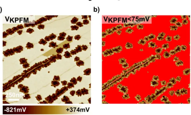
Estimation of the surface coverage of WSe
2Figure S2. (a) KPFM image of the WSe2/Graphene sample (Vtip =VKPFM, surface potential, same image
as the one displayed in Figure 2). (b) Image obtained by keeping the areas for which the SP is lower than 75mV (the areas for which the SP is higher than this threshold are colored in red). This threshold has been fixed accordingly to the SP histogram values (see Figure 2 in the main text). The WSe2 flakes
Supporting Information
Additional cross section profiles
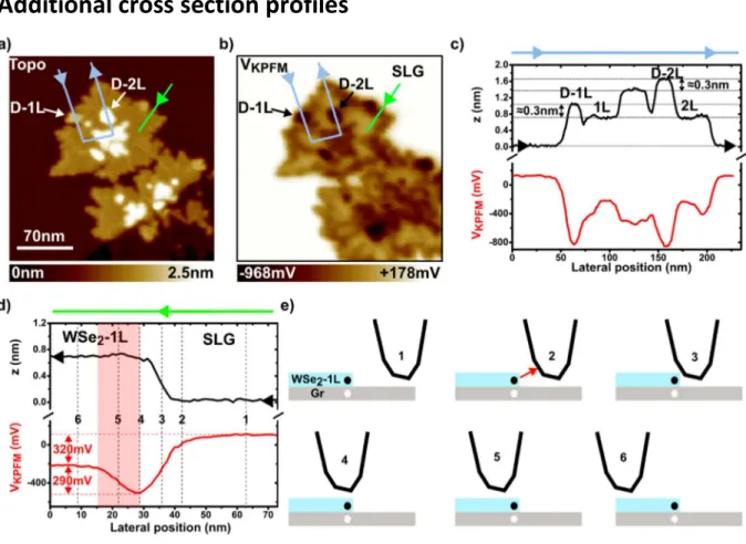
Figure S3. Topographic nc-AFM image (a) and surface potential image (b) of two WSe2 islands located
over SLG (255255nm, same data as the ones shown in Figure 4a,b in the main text). The arrows highlight structural (and charged) defects in the first (D-1L) and second (D-2L) WSe2 layers. (c) Topographic and potentiometric cross-section profiles over structural defects (grey-colored path in the 2D images). (d) Topographic and potentiometric cross-section profiles over the band bending region at the flake’s edge (green-colored path in the 2D images). The semi-transparent red rectangle indicate approximately the location of the band-bending area. (e) Schematic illustration representing 6 different tip-sample positions during the scan over the flake’s edge. Lateral positions compatible with this scheme are indicated by numbered labels in (d). The red arrow in position 2 highlights that in addition to topographic convolution effects, lateral electrostatic forces can induce convolution effects in the SP measurement.
Supporting Information
SLG/TMD and BLG/TMD band diagrams
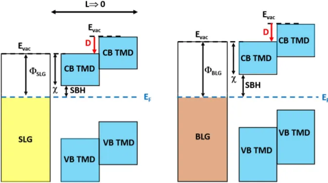
Figure S4. Band diagram of the SLG/TMD and BLG/TMD interfaces. The Schottky Mott rule implies that there should be no electrostatic discontinuity (i.e. no shift of the vacuum level) at the graphene/TMD interfaces. In turn, the charge transfer across the interface (and the resulting dipole, D) induces a shift of the vacuum level. In the case of bulk materials, the equalization of the Fermi levels can be accounted by a band bending region in the vertical direction (an illustration can be found in [11]). In the case of 2D van der Waals interfaces, there is no band bending region in the vertical direction due to the two dimensional nature of the stacked materials. In other words, it is impossible to provide a correct representation of the interface that includes the Schottky Mott configuration at the interface and the vacuum level shift associated to the dipole. This diagram is thus provided only to stress that conceptual difficulty. SLG: single-layer graphene. BKG: bilayer graphene. SBH: Schottky barrier height. : work function. : electron affinity. D: interface dipole. Evac: vacuum level.
Supporting Information
References
[1] Hiura H, Miyazaki H and Tsukagoshi K 2010 Determination of th-e Number of Graphene Layers: Discrete Distribution of the Secondary Electron Intensity Stemming from Individual Graphene Layers
Appl. Phys. Express 3 095101
[2] Park M-H, Kim T-H and Yang C-W 2012 Thickness Contrast of Few-Layered Graphene in SEM: Thickness Contrast of Few-Layered Graphene in SEM Surf. Interface Anal. 44 1538–41
[3] Zhou Y, Fox D S, Maguire P, O’Connell R, Masters R, Rodenburg C, Wu H, Dapor M, Chen Y and Zhang H 2016 Quantitative Secondary Electron Imaging for Work Function Extraction at Atomic Level and Layer Identification of Graphene Sci. Rep. 6 21045
[4] Ferrari A C, Meyer J C, Scardaci V, Casiraghi C, Lazzeri M, Mauri F, Piscanec S, Jiang D, Novoselov K S, Roth S and Geim A K 2006 Raman Spectrum of Graphene and Graphene Layers Phys. Rev. Lett. 97 187401
[5] Fromm F, Oliveira Jr M H, Molina-Sánchez A, Hundhausen M, Lopes J M J, Riechert H, Wirtz L and Seyller T 2013 Contribution of the Buffer Layer to the Raman Spectrum of Epitaxial Graphene on SiC(0001) New J. Phys. 15 043031
[6] Galves L A, Wofford J M, Soares G V, Jahn U, Pfüller C, Riechert H, Lopes J M J 2017 The Effect of the SiC(0001) Surface Morphology on the Growth of Epitaxial Mono-Layer Graphene Nanoribbons
Carbon 115 162–8
[7] Varchon F, Feng R, Hass J, Li X, Ngoc Nguyen B, Naud C, Mallet P, Veuillen J-Y, Berger C, Conrad E H and Magaud L 2007 Electronic Structure of Epitaxial Graphene Layers on SiC: Effect of the Substrate
Phys Rev Lett 99 126805
[8] Melios C, Spencer S, Shard A, Strupiński W, Silva S R P and Kazakova O 2016 Surface and Interface Structure of Quasi-Free Standing Graphene on SiC 2D Mater. 3 025023
[9] Hassan J, Winters M, Ivanov I G, Habibpour O, Zirath H, Rorsman N and Janzén E 2015 Quasi-Free-Standing Monolayer and Bilayer Graphene Growth on Homoepitaxial on-Axis 4H-SiC(0 0 0 1) Layers
Carbon 82 12–23
[10] Bayle M, Reckinger N, Felten A, Landois P, Lancry O, Dutertre B, Colomer J-F, Zahab A-A, Henrard L, Sauvajol J-L and Paillet M 2018 Determining the Number of Layers in Few-Layer Graphene by Combining Raman Spectroscopy and Optical Contrast: Number of Graphene Layers by Combining Raman Spectroscopy and Optical Contrast J. Raman Spectrosc. 9 36–45
[11] Vilan A and Cahen D 2017 Chemical Modification of Semiconductor Surfaces for Molecular Electronics Chem. Rev. 117 4624−66