HAL Id: hal-01316731
https://hal.sorbonne-universite.fr/hal-01316731
Submitted on 17 May 2016
HAL is a multi-disciplinary open access
archive for the deposit and dissemination of
sci-entific research documents, whether they are
pub-lished or not. The documents may come from
teaching and research institutions in France or
abroad, or from public or private research centers.
L’archive ouverte pluridisciplinaire HAL, est
destinée au dépôt et à la diffusion de documents
scientifiques de niveau recherche, publiés ou non,
émanant des établissements d’enseignement et de
recherche français ou étrangers, des laboratoires
publics ou privés.
Distributed under a Creative Commons Attribution| 4.0 International License
High current density GaAs/Si rectifying heterojunction
by defect free Epitaxial Lateral overgrowth on Tunnel
Oxide from nano-seed
Charles Renard, Timothée Molière, Nikolay Cherkashin, José Alvarez, Laetitia
Vincent, Alexandre Jaffré, Géraldine Hallais, James Patrick Connolly, Denis
Mencaraglia, Daniel Bouchier
To cite this version:
Charles Renard, Timothée Molière, Nikolay Cherkashin, José Alvarez, Laetitia Vincent, et al.. High
current density GaAs/Si rectifying heterojunction by defect free Epitaxial Lateral overgrowth on
Tunnel Oxide from nano-seed.
Scientific Reports, Nature Publishing Group, 2016, 6, pp.25328.
www.nature.com/scientificreports
High current density GaAs/Si
rectifying heterojunction by defect
free Epitaxial Lateral overgrowth
on Tunnel Oxide from nano-seed
Charles Renard
1, Timothée Molière
1,2, Nikolay Cherkashin
3, José Alvarez
2, Laetitia Vincent
1,
Alexandre Jaffré
2, Géraldine Hallais
1, James Patrick Connolly
4, Denis Mencaraglia
2&
Daniel Bouchier
1Interest in the heteroepitaxy of GaAs on Si has never failed in the last years due to the potential for monolithic integration of GaAs-based devices with Si integrated circuits. But in spite of this effort, devices fabricated from them still use homo-epitaxy only. Here we present an epitaxial technique based on the epitaxial lateral overgrowth of micrometer scale GaAs crystals on a thin SiO2 layer from
nanoscale Si seeds. This method permits the integration of high quality and defect-free crystalline GaAs on Si substrate and provides active GaAs/Si heterojunctions with efficient carrier transport through the thin SiO2 layer. The nucleation from small width openings avoids the emission of misfit dislocations
and the formation of antiphase domains. With this method, we have experimentally demonstrated for the first time a monolithically integrated GaAs/Si diode with high current densities of 10 kA.cm−2 for a
forward bias of 3.7 V. This epitaxial technique paves the way to hybrid III–V/Si devices that are free from lattice-matching restrictions, and where silicon not only behaves as a substrate but also as an active medium.
Alternative GaAs-on-Si substrates have a considerable market potential for replacing the costly GaAs substrate in producing traditional GaAs-based devices such as solar cells, photodetectors, LEDS, lasers, and microwave devices, and as a new technology for monolithic integration of GaAs elements and Si integrated circuits1–7. The first step toward this goal is to obtain high quality GaAs layer on a Si substrate, creating so-called virtual strates. However, three major problems remain unresolved in GaAs layers grown directly on plain silicon sub-strates, i) the high density of threading dislocations due to the lattice mismatch with Si (around 4%), ii) the formation of anti-phase domains (APDs) due to the polar/non-polar semiconductor interface and iii) the forma-tion of cracks due to the difference in thermal expansion coefficients of GaAs and Si8. Significant improvements have been reported for many years, thanks to selective area epitaxy (SAE) of GaAs on Si substrates patterned with dielectric films9–12. Moreover, even if these deposition procedures can keep the greater part of the epilayer free of defects, the relaxation process of GaAs on silicon leads to the presence of a high density of misfit dislocations located at the interface between Si and GaAs. This renders these layers inappropriate for applications involv-ing carrier transport through the interfacial region. A promisinvolv-ing technique which overcomes these problems is wafer bonding, which is a non-epitaxial method for III–V thin film integration on Si substrates and therefore not subject to the lattice matching limitations associated with epitaxial growth13. Thus, recently Tanabe et al. have obtained promising results with direct fusion bonding of GaAs on Si by successfully obtaining ohmic GaAs/Si highly conductive heterojunction through a 2 nm thick amorphous layer at the GaAs/Si interface5. Nevertheless, such artificial GaAs/Si wafer organization is limited in size by the available III–V substrates, and as the donor GaAs wafer must be eliminated by etching, this technology is considerably more expensive than the epitaxial route14.
1IEF, CNRS, Univ Paris-Sud, Université Paris-Saclay, Orsay, France. 2GeePs, UMR CNRS 8507, CentraleSupelec, Univ
Paris-Sud, Sorbonne Universités, UPMC Univ Paris 06, Université Paris-Saclay, 11 rue Joliot Curie, Plateau de Moulon, 91192, Gif sur Yvette, France. 3CEMES-CNRS and Université de Toulouse, 29 rue Jeanne Marvig, 31055 Toulouse,
France. 4Universidad Politécnica de Valencia, NTC, Camino de Vera s/n. 46022, Valencia, Spain. Correspondence and
requests for materials should be addressed to C.R. (email: charles.renard@u-psud.fr) Received: 08 January 2016
accepted: 15 April 2016 Published: 04 May 2016
OPEN
www.nature.com/scientificreports/
Therefore, the direct epitaxial growth of III–V compounds on Si substrates remains the most desirable approach for III–V/Si hybrid integration. We demonstrate in this paper that the epitaxial lateral overgrowth of GaAs on nano patterned Si substrates with dielectric films appears to be the most promising technique. Thus, if this technique is coupled with the use of a sufficiently small nucleation area size, it is expected to enable the relax-ation of the mismatched material without emission of misfit dislocrelax-ations15. The other advantage of starting from small nucleation areas is to avoid the formation of steps inside nanoseeds, and as the Si surface is monodomain, the growing GaAs crystal cannot form APDs. We have previously demonstrated APDs and dislocation-free GaAs regions grown on thin SiO2 layer where the crystalline order between epi-GaAs and Si substrate was transferred through nano-holes in the SiO2 layer16,17. This first demonstration was done on (001) substrates. In the present paper, we show that some defects remaining on (001) are avoided on (111) orientation. Moreover, a tunneling GaAs/Si heterojunction through the thin SiO2 layer can be expected. We propose to call this growth method ELTOn for Epitaxial Lateral overgrowth on Tunnel Oxide from nano-seed. This integration process presents a promising route to ultrahigh efficiency III–V/Si tandem solar cells with a close to ideal bandgap combination18 which are free from lattice-matching constraints.
Results
GaAs/Si epitaxial growth.
Isolated GaAs microcrystals were grown on (001)Si and (111)Si substrates by the method of Epitaxial Lateral overgrowth on Tunnel Oxide from nano-seed (ELTOn) described in the Methods section of this paper. Their morphology was investigated by transmission electron microscopy (TEM) and their local electrical characterizations were performed by conductive-probe atomic force microscopy (CP-AFM) and Electron Beam Induced Current (EBIC) measurements. Figure 1(a) shows a plane view scanning electron microscopy (SEM) image of several micrometer scale GaAs crystals obtained by ELTOn on (001)Si substrate. Figure 1(b,c) show (001) plane and tilted view SEM images of individual GaAs crystals. The vast majority of GaAs crystals present identical shapes and have 10 {110} facets with a twofold symmetry. This {110}-type orientation is energetically stable and its dominance in faceting can be understood in the nanoscale regime19. Figure 1(d)Figure 1. GaAs/Si epitaxial growth on (001)Si. Plan view of a scanning electron microscopy (SEM) image
of (a) several microscale GaAs crystallites, and (b) zoom of one microscale GaAs crystallite, grown on a (001)Si surface through seeds within a thin SiO2 layer. (c) tilted view around the [110] axis of a microscale GaAs crystallite. (d) Dark-field cross-sectional image of the island taken close to the [110] zone axis of Si with g = − 220. The crystal in bright contrast is in perfect epitaxy with the Si(001) substrate. {111} GaAs twin planes between the central and the left/right parts of the GaAs island are marked by arrows. (e) Schematic representation of the structure of the half of a GaAs island with the identified planes of the facets and twin planes.
www.nature.com/scientificreports/
shows cross-sectional (cs) (110) dark-field image of the GaAs micro-crystals taken close to the zone axis [110] of Si with the diffraction vector g = − 220. According to the diffraction patterns (DPs) taken at different parts of GaAs micro-crystal grown and in the (001)Si substrate (not shown) we have observed that the micrometer scale GaAs crystal is composed of three differently oriented parts, nominally left, central, and right parts. The central part has the direct interface with the Si substrate and is nearly aligned with the Si substrate. The left and the right parts of the islands lying on the surface of the SiO2 layer have twin like orientations with respect to the central part and are clockwise and anticlockwise rotated around the [110] axis by 109.47° with respect to the orientation of the central part. The identification of the GaAs crystal orientation, of the twin and facet planes and the measurement of angles between GaAs crystal edges allows unambiguous reconstruction of the structure of the GaAs island. For the sake of clarity a schematic representation of the structure of half a GaAs μ -crystal (the omitted part has the same mirror symmetry) is shown in Fig. 1(e). In a previous paper16, a simple model was proposed to explain the twin pair formation. One can expect that the twin formation proceeds as soon as the growing crystal reaches the Si to SiO2 boundary, which locally alters the crystalline order. In the [110] direction the growing GaAs crystal can wet the SiO2 layer without perturbation regarding the chemical bond orientations. This also means that lateral growth can spread along the [110] direction to form a vertical (110) external facet. On the contrary, in the [− 110] direction, the As atoms at the edge of the SiO2 layer cannot bind with a fourth bottom Ga atom, and thus exhibit a dangling bond. This frustration would provoke the observed anticlockwise rotation of the GaAs lattice by 109.47° around the [110] direction.
Complementary TEM experiments have also been performed in order to determine the presence or absence of antiphase domains, and as the contrast was found to be homogeneous and unchanged when changing Bragg vectors (from g = 002 to g = 00 − 2), we can deduce that no APDs were present16. Some statistical SEM and TEM analysis of the micrometer scale GaAs/Si(001) crystals exhibiting regular shapes evidence that nucleation from nanoscale openings avoids the formation of APDs and misfit dislocations. Nevertheless, as we have shown, this GaAs on (001)Si growth technique necessarily leads to the creation of twin pairs. This is due to the polar nature of GaAs materials and to the related asymetry between the directions1–10 and [110] which perturbates the ELTOn growth on (001)Si substrate. One way to overcome this problem is to achieve growth on a surface free of this kind of asymetry, such as the (111) surface.
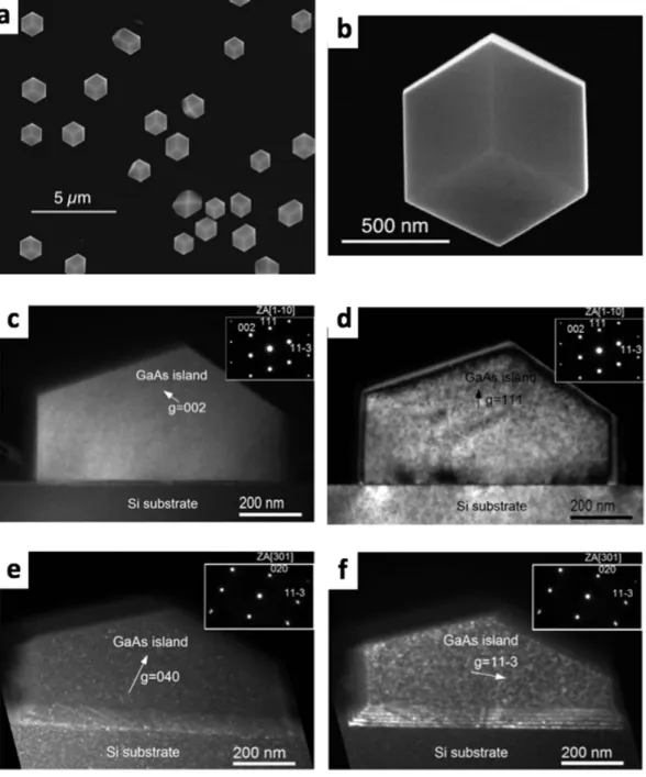
Therefore, the GaAs ELTOn process was also performed on (111)Si wafers. Figure 2(a) shows a plane view SEM image of several micrometer scale GaAs crystal obtained by ELTOn on a (111)Si substrate, and Fig. 2(b) shows a plane view SEM image of an individual GaAs crystal of hexagonal shape with 9 {110} facets. This indi-cates that the equilibrium shape of GaAs crystal on Si is achieved by exhibiting {011} facets that are non-polar surfaces and have a lower surface energy than other facets. Figure 2(c,d) shows the dark-field cross-sectional (1–10) TEM images of the ELTOn GaAs/(111)Si micro-crystal obtained close to the1–10 zone axis at two-beam, exact Bragg conditions with g = 002 (Fig. 2(c)) and g = 111 (Fig. 2(d)). The micrometer scale GaAs crystal is nearly aligned with the Si substrate. From these images we can deduce that neither twins nor APD were formed in the GaAs micro-crystal. Figure 2 (e,f) shows the dark-field weak-beam images of the same crystal obtained by a ≈ 48° rotation around the3–11 axis (indicated in inserts in Fig. 2(c–f)) from the1–10 zone axis and taken close to the [301] zone axis with g = 040 (Fig. 2(e)) and g = 11 − 3 (Fig. 2(f)). Such complementary TEM observations allow to visualize the projected tilted Si/SiO2/GaAs and Si/GaAs interfaces. By using visibility criteria of disloca-tions20, we can indicate the absence of dislocations neither at the interfaces nor within the whole volume of the GaAs micro-crystal. A statistical SEM and TEM analysis concerning micrometer scale GaAs/Si(111) crystals of regular shape enabled to confirm the absence of extended defects within such crystals. Therefore, following this geometry the ELTOn of GaAs leads to a perfect integration of GaAs on Si. It should be noted that the growth temperatures used here are lower than 575 °C. This demonstrates the compatibility of our growth process with the Si CMOS technology platform, as temperature should be preferably limited to a maximum of 600 °C after CMOS processing. Therefore, the epitaxy step can be integrated with the CMOS process without degrading pre-existing MOS device elements. Nevertheless, we have to keep in mind that the CMOS process is limited to 001-oriented substrates. We have now to investigate if this stacking is appropriate for applications involving electronic trans-port through the interfacial region.
Local electrical characterizations of GaAs/Si microscale islands.
It should be noted that the SiO2 layer between the GaAs/Si interface has a thickness of around 0.6 nm for (001)Si, and of 1.2 nm for (111)Si. Tanabe et al. have previously shown that GaAs directly bonded on Si substrate through an amorphous layer up to 2 nm thick can lead to a highly conductive heterojunction5. Therefore, the SiO2 thicknesses used for the present study are sufficiently thin to provide high interfacial conductivity via tunneling21,22.
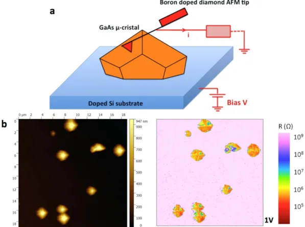
To check this point, local electrical characterizations of GaAs/Si microscale islands were performed by CP-AFM23–26. In addition to CP-AFM, EBIC has also been applied to electrically map the GaAs/Si cross-section.
AFM measurements were performed simultaneously in the topographical mode and in the conductive-probe mode (Resiscope
™
). By applying a voltage bias between the substrate and the conducting cantilever, a current is generated. This current can be used to construct a spatially resolved conductivity image. It also allows for local current vs voltage measurements (I–V) with purely topographic feedback and high resolution. These measure-ments were very useful to investigate the local electrical behaviour of GaAs/Si-substrate heterojunctions. The CP-AFM details and more specifically the sample configuration and biasing are displayed in Fig. 3a. The DC bias voltage was applied through the doped silicon wafer. Figure 3b depicts a 20 × 20 μ m2 surface map that illustrates, from left to right, the topography and the electrical properties of n.i.d (non-intentionaly doped) GaAs μ -crystals obtained by ELTOn process. The brightest spots (highest features) in the topography image represent the GaAs μ -crystals that are well correlated with the conductive yellow-green spots in the electrical image obtained for an applied voltage of + 1V. This last image results from an average of the electrical images scanned in trace and retrace directions to minimize the closed loop faults that can induce the topography of the μ -crystals. In order towww.nature.com/scientificreports/
get more precise information about the variation of the local resistance as a function of the applied bias, CP-AFM was locally used to investigate I–V characteristics on individual GaAs μ -crystals grown on Si(001) and Si(111). Figure 4 displays a semi-log plot of the I–V characteristics, from left to right, of ELTOn GaAs μ -cristals grown on (001) p(B)-Si wafer (3.3 × 10¹⁵–4.5 × 1015 cm−3) and on (111) n(P)-Si wafer (1.1 × 10¹⁶ − 8.3 × 1016 cm−3). Figure 4a,b revealed rectifying properties and non-ohmic behavior (diode-like) with currents as high as 1.3 × 10⁻⁴ A and 4.2 × 10⁻⁵ A under forward bias, respectively, for n-doped (111)Si and p-doped (001)Si. These rectifying behaviours were observed for all the analyzed μ -crystals and evidenced for different AFM tips in terms of electrical coating (platinum silicide and Pt-Ir). Statistically, all the GaAs show a rectifying behaviour, and identical forward and reverse currents were also observed for GaAs μ -cristals presenting similar shape and size. Nevertheless, some differences were observed for the reverse current pointing out multiple origins (μ -crystal and tunnel-oxide areas, quality of electrical contact between the AFM tip and the μ -crystal, etc) that are still
Figure 2. GaAs/Si epitaxial growth on (111)Si. Plan-view of a scanning electron microscopy (SEM) image
of: (a) several microscale GaAs crystallites and (b) zoom of one microscale GaAs crystallite, grown on a (111) Si surface through the seeds within a thin SiO2 layer. (c–f) Dark-field cross-sectional (1–10) TEM images of the ELTOn GaAs/(111)Si micro-crystal obtained at two-beam conditions: (c)1–10 zone axis, g = 002, exact Bragg conditions; (d)1–10 zone axis, g = 111, exact Bragg conditions; (e) [301] zone axis, g = 040, (g, + 2g) weak-beam conditions; (f) zone axis [301], g = 11–3, (g, + 2g) weak-beam conditions. (e) and (f) were obtained by a ∼ 48° rotation around the3–11 axis from the1–10 zone axis.
www.nature.com/scientificreports/
under investigation. In order to further characterize the GaAs/Si-substrate heterointerfacial electrical properties, complementary EBIC measurement was also performed on ELTOn GaAs micro-crystals on Si wafers. Two con-tacts were taken with nano-tips on the sample, the top one on the GaAs micro-crystal and the lower one on the side of the Si wafer. As expected, the p-n heterojunction between GaAs micro-crystal and Si substrate exhibits an internal electric field (which induces to the observed EBIC current by separating e-beam generated electron–hole pairs). This is shown in Fig. 5 displaying the EBIC contrast around the GaAs and Si interface superimposed with the SEM structural image of a GaAs micro-crystal grown on (111) n-Si. The EBIC map indicates that the current crosses uniformly through the whole interface between Si subtrate and ELTOn GaAs micro-crystal including the germination hole and the oxide area. This confirms that the GaAs/Si heterojunction through the thin SiO2 layer is conductive. Moreover, I–V characteristics obtained from EBIC are comparable to those obtained by CP-AFM. As the current crosses uniformly through the GaAs/Si interface, we can deduce current densities from the contact
Figure 3. Conductive probe–AFM measurements. (a) Sketch illustrating the details of CP-AFM
measurements on GaAs μ -cristal obtained by ELTOn process. (b) 20 × 20 μ m2 surface map illustrating the topography (left side) and the local resistance (right side) of GaAs μ -cristal obtained by ELTOn process on (001) p-Si wafers ([B] = 3.3–4.5 × 1015 cm−3).
Figure 4. I–V measurements. I–V characteristics, measured by CP-AFM, of the ELTOn GaAs/Si μ -crystal on
www.nature.com/scientificreports/
area between GaAs μ -crystal and SiO2 layer. Current densities as high as 10 kA.cm−2 and 2.5 kA.cm−2, respec-tively for n-doped (111)Si and p-doped (001)Si, have been measured in forward bias. These current densities val-ues are much higher than those obtained by direct GaAs/Si bonding technique5,27 and are comparable with those obtained for Si-InAs heterojunction fabricated by growing InAs nanowires in oxide mask openings on silicon28,29.
GaAs/Si heterojunction modelling.
In order to determine the (non intentional) doping level of our GaAs micro-crystal, calculations of I–V characteristics of the GaAs/Si heterojunction with varying doping concentra-tions of GaAs have been performed, and compared to experimental I–V characteristics. The SILVACO model-ling30 uses numerical solutions extensively described in the literature and well adapted to this system. The aim of this numerical modelling is to establish the likely polarity and density of net doping in the GaAs crystals, and to qualitatively reproduce the trends observed under forward and reverse bias. The junction area is estimated from the micrographs and is set at 1 μ m2 in the simulations, and the height of the GaAs crystal is set to 1 μ m. The modelling is insensitive to the thickness of the Si region, which is therefore set to 10 μ m for computational reasons rather than the experimental thickness of 200 μ m.The modelling assumes that the GaAs doping level must be the same for ELTOn GaAs μ -cristals grown on (001) p(B)-Si wafers and on (111) n(P)-Si wafers. A good agreement is found for a p-type doping in the 1015– 1016 cm−3 range in ELTOn GaAs μ -crystal. This low p-type doping level is in agreement with the value already reported by Kikkawa et al., for growth conditions pretty close to ours, in terms of temperature and V/III ratio with the use of TMGa and TBAs precursors31.
Conclusion
In conclusion, we have proposed a technique to grow epitaxially high quality microscale GaAs crystals on Si subtrate. This method is based on the GaAs chemical beam lateral epitaxy from nanoscale Si seeds opened through a very thin SiO2 layer. As a tunnel junction is expected between the GaAs micro crystal and the Si, we have proposed to call this technique ELTOn for Epitaxial Lateral overgrowth on Tunnel Oxide from nano-seed. Transmission electron microscopy have revealed that ELTOn GaAs microcristals grown on (111)Si are perfectly integrated and defect free. Those grown on (001)Si contain only a pair of {111} twin planes sectioning their vol-ume into a central part quasi-similarly oriented with the Si substrate and into two mirror twinned ones. We have experimentally shown that ELTOn GaAs micro-crystals form highly conductive rectifying junctions with the Si substrate whatever its orientation. We have then demonstrated for the first time a monolithically integrated GaAs/ Si diode with a current as high as 10 kA.cm−2. Finally, a doping level of 1015–1016 cm−3 range in GaAs micro-scale islands was found to account for the I–V characteristics measured with complementarily doped Si substrates.
Therefore, in comparison with other typical hetero-epitaxial methods of III–V growth on Si, the ELTOn method appears as very promising for monolithic integration of III–V semiconductor on Si, where Si not only behaves as a substrate but also as an active medium. For the purpose of developing electronic devices, the devel-opment of localized nano-seeds, as well as post-epi planarization process is now under develdevel-opment.
Methods
Epitaxial growth.
The Epitaxial Lateral overgrowth on Tunnel Oxide from nano-seed (ELTOn) technique proposed here was carried out in a chemical beam epitaxy system with a base pressure of 2 × 10⁻⁸ Pa. Pure silane (SiH4), trimethylgallium (TMGa) and tertiarybutylarsine (TBAs) were used as gas sources. The (001) p(B)-Si wafers (3.3 × 10¹⁵–4.5 × 1015 cm−3) and (111) n(P)-Si wafers (1.1 × 10¹⁶– 8.3 × 1016 cm−3) were cleaned using the modified Shiraki chemical cleaning32 which results in a reproducible 0.6 nm for (001)Si, resp. 1.2 nm for (111)Si,Figure 5. Electron beam induced current map. EBIC map superimposed with the SEM structural image of
www.nature.com/scientificreports/
thick oxide layer (deduced from Auger electron spectrometry and HRTEM). After this chemical cleaning step, the substrates were slowly annealed in situ up to 650 °C, the pressure being maintained below 3 × 10⁻⁶ Pa.
Prior to GaAs epitaxy, the nucleation seeds must be created. In order to open nanoscale holes through the thin silica layer, the oxidized substrate was exposed to a silane partial pressure of 0.66 Pa at a temperature less than 650 °C during 4 min for Si(001) and 1 min 30 s for Si(111). That results in pure Si nano-areas formed via the reduction of SiO2 into volatile SiO. This method which has been detailed elsewhere33 has the advantage of easily providing nanoscale seeds around 50 nm in width, randomly spaced at the surface of the oxidized Si substrate. After this step, the GaAs epitaxy was initiated with the well-known two step procedure8. The first step consists in introducing solely TBAs (during 2 min) under a total pressure of 1.32 Pa at 430 °C. In the second step TMGa was also introduced and the total pressure was increased up to 6.6 Pa achieving a V/III ratio of [TBAs]/[TMGa] = 6, while the growth temperature was increased up to 550 °C for (001)Si and 575 °C for (111)Si, respectively. After this sequence that tooks 2 min, GaAs epitaxial lateral overgrowth was then continued for 40 min.
Structural characterisation.
The surface morphology of micrometer scale GaAs crystals was characterized by scanning electron microscopy (SEM) (Hitachi SU8000) and the structural and crystalline quality of microme-ter scale GaAs were further investigated by cross-sectional transmission electron microscopy (TEM) using a Jeol 2010 TEM operating at 200 kV, from lamellas prepared by gallium focused ion beam (Ga-FIB) milling.Conductive-probe AFM measurements.
Local electrical measurements of GaAs/SiO2/Si micro-structures were investigated with conductive-probe AFM (CP-AFM) and were performed using a Digital Instruments Nanoscope IIIa Multimode AFM associated with the home-made conducting probe extension called “Resiscope™
”23. This setup allows us to apply a stable DC bias voltage (from − 10 to + 10 V by 0.01 V steps) to the device and to measure the resulting current flowing through the tip as the sample surface is scanned in con-tact mode. Local resistance values can be measured in the range of 102–1012 Ω, which allows investigations on a variety of materials34,35 and devices25,36. Measurement accuracy based on calibrations is below 3% in the range of 102–1011 Ω, and it can reach 10% for higher resistance values. In this paper, a boron-doped diamond AFM tip has been used for the local current vs voltage measurements.Electron beam induced current measurements.
Electron beam induced current (EBIC) measurements have been performed on GaAs/Si heterojunctions in a Hitachi SU8000 SEM equipped with a Gatan EBIC system (SmartEBIC) and in-situ nanomanipulators for the electric conctact. This technique employs an electron beam to induce a current within the sample which is used as a signal for generating images that depict the electrical behaviour of the sample. With proper electrical contacts the movement of the holes and electrons generated by the SEM’s electron beam can be collected, amplified, analyzed, and displayed as variations of contrast in an EBIC image. Samples were polished on the edge. Two tungsten micro-tips supported by micromanipulators enable in the SEM, to contact the upper top of a GaAs cristal and the backside of the Si substrate, and to collect I(V) curves or induced current. The electron beam is scanned perpendicular to the cross section i.e. perpendicular to the normal of the substrate. The electron beam acceleration voltage was set to 25 keV and extraction at 5 μ A giving a current on the sample around 150 pA.GaAs/Si Modeling.
SILVACO modeling30 was also used in order to qualitatively reproduce the trends observed for experimental I(V) under forward and reverse bias. Materials parameters used in the simulations use default values in the Silvaco ATLAS manual, appendix B “Materials Parameters” for 300 K standard test conditions. Important GaAs values for this problem are the bandgap of Eg(GaAs) = 1.42 eV, electron affinity χ (GaAs) = 4.07 eV, and relative permittivity ε (GaAs) = 13.2. The equivalent values for Si are Eg(Si) = 1.08 eV, electron affinity χ (GaAs) = 4.05 eV, and relative permittivity ε (GaAs) = 11.8.References
1. Zahler, J. M. et al. High efficiency InGaAs solar cells on Si by InP layer transfer. Appl. Phys. Lett. 91, 012108 (2007).
2. Lueck, M. R. et al. Dual junction GaInP/GaAs solar cells grown on metamorphic SiGe/Si substrates with high open circuit voltage, IEEE Electron Devices Lett. 27, 142 (2006).
3. Maruyama, T. et al. GaInAsP/InP membrane BH-DFB lasers directly bonded on SOI substrate. Opt. Express 14, 8184 (2006). 4. Chriqui, Y. et al. Long wavelength room temperature laser operation of a strained InGaAs/GaAs quantum well structure
monolithically grown by metalorganic chemical vapour deposition on a low energy-plasma enhanced chemical vapour deposition graded misoriented Ge/Si virtual substrate. Opt. Mater. 27, 46 (2005).
5. Tanabe, K., Watanabe, K. & Arakawa, Y. III-V/Si hybrid photonic devices by direct fusion bonding, Scientific Reports. 2, 349 (2012). 6. Lew, K. L. et al. High gain AlGaAs/GaAs heterojunction bipolar transistor fabricated on SiGe/Si substrate. J. Vac. Sci. Technol. B. 25,
902 (2007).
7. Wu, Y. Q. et al. Atomic-layer-deposited Al2O3/GaAs metal-oxide-semiconductor field-effect transistor on Si substrate using aspect ratio trapping technique. Appl. Phys. Lett. 93, 242106 (2008).
8. Fang, S. F. et al. Gallium arsenide and other compound semiconductors on silicon. J. Appl. Phys. 68, R31 (1990).
9. Li, J. Z. et al. Defect reduction of GaAs epitaxy on Si(001) using selective aspect ratio trapping. Appl. Phys. Lett. 91, 021114 (2007). 10. Li, J. Z. et al. Defect reduction of GaAs/Si epitaxy by aspect ratio trapping J. Appl. Phys. 103, 106102 (2008).
11. Deura, M. et al. Effect of Ga content on crystal shape in micro-channel selective-area MOVPE of InGaAs on Si. Journal of Crystal Growth 310, 4768 (2008).
12. Hsu, C.-W., Chen, Y.-F. & Su, Y.-K. Nano epitaxial growth of GaAs on Si(001). Appl. Phys. Lett. 99, 133115 (2011). 13. Tong, Q.-Y. & Gosele, U. Semiconductor wafer bonding: Science and technology (Wiley, New Jersey, 1998).
14. Bolkhovityano, Y. B. & Pchelyakov, O. P. III–V Compounds-on-Si: Heterostructure Fabrication, Application and Prospects. The Open Nanoscience Journal 3, 20 (2009).
15. Luryi, S. & Suhir, E. New approach to the high quality epitaxial growth of lattice-mismatched materials. Appl. Phys. Lett. 49, 14 (1986).
www.nature.com/scientificreports/
16. Renard, C. et al. Dislocation and antiphase domain free microscale GaAs crystals grown on SiO2 from (001)Si nano-areas. Appl.
Phys. Lett. 102, 191915 (2013).
17. Renard, C. et al. Growth of high quality micrometer scale GaAs/Si crystals from (001)Si nano-areas in SiO2. Journal of Crystal
Growth 401, 554 (2014).
18. Connolly, J. P., Mencaraglia, D., Renard, C. & Bouchier, D. Designing III–V multijunction solar cells on silicon. Prog. Photovolt: Res. Appl. 22, 810 (2014).
19. Lee, S. C. & Brueck, R. J. Equilibrium crystal shape of GaAs in nanoscale patterned growth J. Appl. Phys. 96, 1214 (2004). 20. Cherkashin, N. & Claverie, A. In book: Transmission Electron Microscopy in Micro-nanoelectronics, Chapter: Characterization of
Process-Induced Defects, pp. 165–193 (2012), Publisher: WILEY, ISBN: 9781848213678 Editors: Claverie, A.
21. Rosenbaum, E. & Register, L. F. Mechanism of stress-induced leakage current in MOS capacitors. IEEE Trans. Electron. Dev. 44, 317 (1997).
22. Miranda, E., Sune, J., Rodriguez, R., Nafria, M. & Aymerich, X. Soft Breakdown Fluctuation Events in Ultrathin SiO2 Layers. Appl.
Phys. Lett. 73, 490 (1998).
23. Houzé, F., Meyer, R., Schneegans, O. & Boyer, L. Imaging the local electrical properties of metal surfaces by atomic force microscopy with conducting probes. Appl Phys Lett 1996, 69 (1975).
24. Houzé, F., Chrétien, P., Schneegans, O., Meyer, R. & Boyer, L. Simultaneous resistance and capacitance cartography by conducting probe atomic force microscopy in contact mode. Appl. Phys. Lett 86, 123103 (2005).
25. Alvarez, J., Houzé, F., Kleider, J.-P., Liao, M. Y. & Koide, Y. Electrical characterization of Schottky diodes based on boron doped homoepitaxial diamond films by conducting probe atomic force microscopy. Superlatt Microstruct 40, 343 (2006).
26. Schneegans, O., Houzé, F., Chrétien, P. & Meyer, R. Capacitance measurements on small parallel plate capacitors using nanoscale impedance microscopy, Appl. Phys. Lett. 90, 043116 (2007).
27. Liang, J. et al. Electrical Properties of p-Si/n-GaAs Heterojunctions by Using Surface-Activated Bonding. Applied Physics Express 6, 021801 (2013).
28. Björk, M. T. et al. Si–InAs heterojunction Esaki tunnel diodes with high current densities. Applied Physics Letters 97, 163501 (2010). 29. Riel, H. et al. InAs–Si nanowire heterojunction tunnel FETs. Electron Device Letters, IEEE 33, 1453 (2012).
30. ATLAS User’s Manual: Device Simulation Software, 2014. Santa Clara, SILVACO International.
31. Kikkawa, T., Tanaka, H. & Komeno, J. The growth of GaAs, AlGaAs, and selectively doped AlGaAs/GaAs heterostructures by metalorganic vapor phase epitaxy using tertiarybutylarsine. J. Appl. Phys. 67, 7576 (1990).
32. Gallas, P., Berbezier, I. & Derrien, J. Homoepitaxy of silicon at low temperature on clean and Ga-covered substrates. Thin Solid Films
294, 69 (1997).
33. Halbwax, M. et al. Epitaxial growth of Ge on a thin SiO2 layer by ultrahigh vacuum chemical vapor deposition. Journal of crystal
Growth, 308, 26 (2007).
34. Kleider, J.–P., Longeaud, C., Brüggemann, R. & Houzé, F. Electronic and topographic properties of amorphous and microcrystalline silicon thin films. Thin Solid Films 57, 383 (2001).
35. Planès, J., Houzé, F., Chrétien, P. & Schneegans, O. Conducting probe atomic force microscopy applied to organic conducting blends. Appl. Phys. Lett. 79, 2993 (2001).
36. Alvarez, J., Kleider, J.-P., Houze, F., Liao, M.–Y. & Koide, Y. Local photoconductivity on diamond metal-semiconductor-metal photodetectors measured by conducting probe atomic force microscopy. Diamond Relat Mater 16, 1074 (2007).
Acknowledgements
This work was supported by the french Agence Nationale de la Recherche (ANR MULTISOLSI project, Convention n° ANR 2011 PRGE 009 01). The authors also thank the “Centrale de Technologie Universitaire” MINERVE and RENATECH for technological backup.
Author Contributions
C.R. conceived and supervised the research and helped T.M. and G.H. for epitaxial lateral overgrowth of GaAs on thin SiO2 layer and technological process. J.A. and A.J. performed the CP-AFM measurement. L.V. performed the EBIC measurement. T.M. performed the MEB imaging. N.C. prepared the TEM sample and performed the imaging. J.P.C. and D.M. performed the SILVACO modelling. C.R. and D.B. wrote the paper. All authors discussed the results and commented on the manuscript.
Additional Information
Competing financial interests: The authors declare no competing financial interests.
How to cite this article: Renard, C. et al. High current density GaAs/Si rectifying heterojunction by defect
free Epitaxial Lateral overgrowth on Tunnel Oxide from nano-seed. Sci. Rep. 6, 25328; doi: 10.1038/srep25328 (2016).
This work is licensed under a Creative Commons Attribution 4.0 International License. The images or other third party material in this article are included in the article’s Creative Commons license, unless indicated otherwise in the credit line; if the material is not included under the Creative Commons license, users will need to obtain permission from the license holder to reproduce the material. To view a copy of this license, visit http://creativecommons.org/licenses/by/4.0/