HAL Id: hal-01383737
https://hal.inria.fr/hal-01383737
Submitted on 19 Oct 2016
HAL is a multi-disciplinary open access
archive for the deposit and dissemination of
sci-entific research documents, whether they are
pub-lished or not. The documents may come from
teaching and research institutions in France or
abroad, or from public or private research centers.
L’archive ouverte pluridisciplinaire HAL, est
destinée au dépôt et à la diffusion de documents
scientifiques de niveau recherche, publiés ou non,
émanant des établissements d’enseignement et de
recherche français ou étrangers, des laboratoires
publics ou privés.
Distributed under a Creative Commons Attribution| 4.0 International License
Laser-Induced Fault Effects in Security-Dedicated
Circuits
Vincent Beroulle, Philippe Candelier, Stephan de Castro, Giorgio Di Natale,
Jean-Max Dutertre, Marie-Lise Flottes, David Hely, Guillaume Hubert, R.
Leveugle, Feng Lu, et al.
To cite this version:
Vincent Beroulle, Philippe Candelier, Stephan de Castro, Giorgio Di Natale, Jean-Max Dutertre, et al..
Laser-Induced Fault Effects in Security-Dedicated Circuits. VLSI-SoC: Very Large Scale Integration
and System-on-Chip, Oct 2014, Playa del Carmen, Mexico. pp.220-240,
�10.1007/978-3-319-25279-7_12�. �hal-01383737�
Laser-Induced Fault Effects in Security-Dedicated
Circuits
V. Beroulle3, P. Candelier6, S. De Castro2,5, G. Di Natale2, J.-M. Dutertre5, M.-L. Flottes2, D. Hély3, G. Hubert4, R. Leveugle1, F. Lu2, P. Maistri1, A. Papadimitriou3, B.
Rouzeyre2, C. Tavernier6, P. Vanhauwaert1
(1) Univ. Grenoble Alpes, TIMA, F-38000 Grenoble, France (1) CNRS, TIMA, F-38000 Grenoble, France
(2) Université Montpellier/CNRS UMR 5506, LIRMM, Montpellier, France (3) Univ. Grenoble Alpes, LCIS, F-26000 Valence, France
(4) ONERA, Toulouse, France
(5) Ecole Nat. Sup. des Mines de Saint-Etienne, CMP, LSAS, Gardanne, France (6) STMicroelectronics, France
Abstract. Lasers have become one of the most efficient means to attack secure
integrated systems. Actual faults or errors induced in the system depend on many parameters, including the circuit technology and the laser characteristics. Understanding the physical effects is mandatory to correctly evaluate during the design flow the potential consequences of a laser-based attack and implement efficient counter-measures. This paper presents results obtained within the LIESSE project, aiming at defining a comprehensive approach for designers. Outcomes include the definition of fault/error models at several levels of ab-straction, specific CAD tools using these models and new counter-measures well-suited to thwart laser-based attacks. Actual measures on components man-ufactured in the new 28nm FDSOI technology are also presented.
Keywords: Hardware security, Fault attacks, Lasers, Fault models, Security
evaluation, Counter-measures.
1
Introduction
Hardware attacks on secure integrated systems can be done by several means, includ-ing side-channel observation (measurinclud-ing e.g., computation time, power consumption or electromagnetic emissions) and faulty behavior exploitation. We will focus here on fault-based attacks aiming at retrieving some confidential information such as a pri-vate cryptographic key stored in the circuit. One of the most efficient techniques to induce faults in a circuit is to use a laser [1].
Since the pioneer work by Skorobogatov and Anderson [2], many experimental works have been done on laser-based attacks on various types of circuits, including smartcards but also FPGAs. However, a clear view of laser effects is still lacking [1]. From a designer point-of-view, it is therefore difficult to understand the exact
protec- 978-1-4799-6016-3/14/$31.00 ©2014 IEEE
tions ("counter-measures") to implement in a circuit, and also to identify the most critical parts in a given design.
The work presented here aims at providing a more comprehensive framework to designers. One part of the proposal concerns the definition of models representing the effects of laser attacks with several levels of abstraction. The second part concerns specific counter-measures that can be selected to increase the robustness. The design-er work is also supported by specific design tools.
In this chapter, section 2 is dedicated to laser-silicon interaction. Section 3 gives an overview of the global modeling and design flow from a laser-based attack perspec-tive. Section 4 summarizes results obtained by actual laser attacks, especially on components in the new 28nm FDSOI technology. Section 5 discusses the fault and error models. Section 6 is dedicated to the CAD tools and section 7 shows new coun-ter-measures adapted to the effects of laser-based attacks.
2
Laser/Silicon interaction
2.1 Photoelectric effect
When light emitted by a laser hits a CMOS device, its energy is turned into electrical current thanks to the photoelectric effect. Provided that the energy of the photons emitted by the laser is sufficient, these photons create electron/hole pairs along their path through the silicon (the so-called photoelectric effect).
A current is the result of charges moving. As a consequence of the photoelectric ef-fect, two mechanisms put the charges created by the laser in movement and therefore induce a transient current. A reverse biased PN junction (drain tied to Vdd, P-substrate tied to Gnd) is taken as example in Fig. 1 to present these mechanisms.
Fig. 1. The mechanism responsible for Optical Beam Induced Current [3]
The biasing enlarges the space charge region at the interface between P and N re-gions. As the laser beam goes through the PN junction and the silicon, it creates elec-tron/hole pairs. Then the charges that are close enough to the junction are moved (at-tracted or repulsed depending on the charge) by the effect of both the electric field and the diffusion effect. The charges that are far from the junction recombine them-selves without any effect on the induced current at the drain of the junction.
Fig. 2. Typical shape of nodal current at a p-n junction [4]
Fig. 2 shows the typical shape of the induced transient current at the drain node creat-ed by the laser. The electric field and the diffusion effects can be differentiatcreat-ed on the shape. The prompt collection corresponding to the electric field effect induces a high current during a short time. The diffusion-induced current has low amplitude that lasts longer than the prompt collection. This is due to the speed of the diffusion phenome-non in silicon.
Equation (1) represents the general equation of the current shape observed in Fig. 2.
(1) [5]
With Q the charge deposited by the laser strike, τa the collection time constant which is a process-dependent collection time constant of the junction and τb is the ion-track establishment time constant which is relatively independent of the technology. Typi-cal value of τa and τb can be found in [6].
The induced current can be high enough to temporarily invert the output of a logic cell, thus possibly generating an error in the circuit. The following subsection details how faults can be generated within a digital circuit, by means of a laser injection.
2.2 Single Event Transient (SET) and Single Event Upset (SEU)
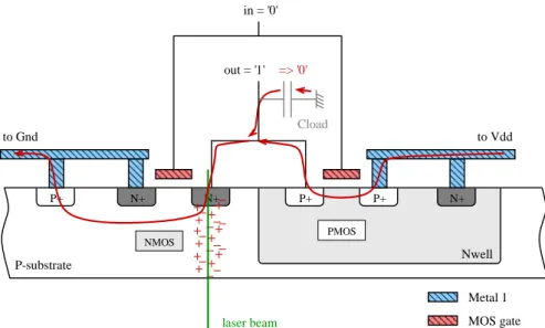
The mechanism by which the induced current changes a logic value is presented in Fig. 3. An inverter gate is taken as an example.
Let assume the input of the inverter being equal to the logic value ‘0’, therefore its output being ‘1’. By assuming to be in stationary conditions, the equivalent output capacitance Cload(i.e., the sum of all gate capacitances of cells connected to this output) is fully charged.
If a laser beam reaches the drain of the NMOS transistor in OFF mode (i.e. a re-verse biased PN junction as exemplified in subsection 2.1), then a transient current is generated between the drain and the bulk node. This current makes electrons move from both Vdd and the equivalent output capacitance toward Gnd.
Fig. 3. Effect of the laser-induced photocurrent (red arrows) on an inverter gate
As a consequence, the output capacitance may be discharged provided that the photo-current is higher than the photo-current flowing through the PMOS transistor. The duration of this effect depends on the injection time. If the illumination duration is large enough, the output capacitance can be discharged at the point where its voltage falls under the threshold voltage of the next logic gates, thus causing a logic fault.
Logic faults can have different effects based on the target cell. If the laser illumi-nates a combinational gate (e.g. Fig. 4(a)), the erroneous transient value generated at the output of the gate must reach the downstream memory cell during the memoriza-tion time-window of that cell in order to affect the circuit behavior and propagate through the circuit at the next clock cycle. This kind of effect is called Single Event Transient (SET).
Fig. 4. (a) SET, and (b) SEU mechanisms
N+ N+ N+ laser beam Metal 1 MOS gate Nwell Cload in = '0' out = '1' => '0' to Vdd to Gnd P-substrate P+ P+ P+ NMOS PMOS
Conversely, when the laser bean directly affects the memory cell (Fig. 4 (b)), there are no timing constraints to induce an error. Indeed, the logic value stored in the memory cell can be directly flipped (the so-called Single Event Upset: SEU) and propagates through the logic during the next clock cycle.
3
Global Flow: Overview
Fig. 5. Global flow: Modeling and Design
Modeling and design flows are illustrated in Fig. 5, resp. left and right sides. Model-ing has to be made once for a given technology and a given spectrum of laser sources and parameters. In fact, some models may be re-used from one technology to another, but new experimental measures are required to calibrate the probability of a given type of fault/error, for a given source and a given technology. Low-level physical models (or TCAD models) are derived from the analysis of the interaction between the laser beam and the circuit material. Such models are very long to simulate, so more abstract models based on current curves must be derived in order to perform simulations at the electrical level. Abstraction can then be raised again at the logical level for gate-level netlist simulation. Finally, behavioral error models corresponding to data perturbations can be proposed for early design analysis. This bottom-up pro-cess, validated by the experiments performed on real circuits, lead to a set of models adapted to several design steps.
Once the models are available, a designer can perform various analyses at several design steps. Early analyses can be made after the Register-Transfer level description, using either behavioral simulation or emulation, and injecting errors corresponding to the behavioral models. This first analysis may allow him to quantify the probability of a successful attack from a functional point of view and identify some weak points in the design (including or not some functional counter-measures). On this basis, coun-termeasures may be added to the design at several levels, from functional checks down to e.g., placement and routing constraints or sensor insertions. Further analyses can then be performed once the gate-level netlist is available, and then when the placement and routing has been done, with potentially electrical-level simulations using the previously developed fault models. All these steps must maximize the
prob-ability that the final qualifications made on the first product prototypes confirm a satisfying level of resilience against attacks.
4
Measures on Bulk and FDSOI components
Measures from actual experiments using a laser are mandatory to develop and assert the validity of physical and electrical models. Previous related work was done in or-der to or-derive models of laser shots on CMOS Bulk ICs, especially on SRAM cells [7]. The model validity was assessed by a very good correlation with an experimental laser sensitivity map.
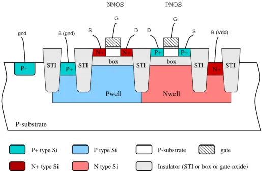
Our current modeling work is focused on the emerging 28nm Fully Depleted Sili-con On Insulator (FDSOI) technology. FDSOI is mainly dedicated to low-power ap-plications and provides thanks to well biasing techniques the ability to optimize dy-namically the circuit’s speed versus its power consumption [8]. FDSOI is also ex-pected to bring reduced sensitivity to laser attacks due to the thin oxide box that iso-lates the channel of transistors from their wells [9]. This feature of FDSOI transistors is illustrated in Fig. 6, in which the cross sectional view of both NMOS and PMOS is drawn.
Fig. 6. Cross sectional view of NMOS (left) and PMOS (right) regular Vt transistors in 28nm FDSOI technology (note that dimensions are not drawn at scale for readability pur-poses).FDSOI transistors are built on a thin isolation box (less than 30 nm) that iso-lates their channel and diffusions (both source and drain) from the corresponding well. The channel of 28nm FDSOI transistors is made of intrinsic silicon; its thickness is less than 10nm. As a consequence, because of the isolation box, charge carriers
Nwell Pwell P+ P-substrate P+ type Si box P+ P+ box N+ N+ N+ P+
Insulator (STI or box or gate oxide) N+ type Si
P type Si P-substrate gate
G S D D S G NMOS PMOS B (gnd) B (Vdd) gnd N type Si
STI STI STI STI
induced by a laser shot outside the transistor cannot contribute to a transient current at the origin of a SET or SEU. Only charge carriers induced inside a transistor, which has a reduced volume, may create a transient current. The related phenomenon is significantly different from that described in Fig.1 for bulk CMOS, for which charge carriers induced outside the transistor itself may contribute to the photocurrent. As a result, the induced photocurrent should be reduced both in magnitude (fewer charges are collected) and in time (because the diffusion component of a photocurrent, as drawn in Fig. 2, will not be collected due to the isolation box).
For the purpose of validating the assumption of reduced laser sensitivity of FDSOI technology and of building a simulation model we measured the laser-induced photo-current on FDSOI test patterns (transistors of various types and sizes). We used the following laser settings: 1064nm wavelength, 20 µs pulse duration, 5 µm spot diame-ter and backside illumination.
Fig. 7. Laser induced photocurrent magnitude [µA] in the drain diffusion of transistors #1 and
#2 in OFF state as a function of the distance [µm] between the laser spot and the transistor’s center
We report here the experiments carried out on two thick oxide high voltage NMOS transistors denoted #1 and #2 hereafter. Transistor #2’s area is three times that of transistor #1. The transistors were biased in OFF state: Vdrain=1.8V,
Vsource=Vgate=VPwell = 0V. The laser pulse power was set to 855mW. We measured the
peak magnitude of the photocurrent pulse induced by a laser shot in the drain of the transistor as a function of the distance between the laser spot and the center of the transistor. The corresponding curves are given in Fig. 7. The maximum magnitude is found for a laser spot located on the transistor’s center (distance equals to zero in Fig. 7): 8µA for transistor #1 and 27µA for transistor #2. Then, as the distance is in-creased, the current magnitude decreases. It tends almost toward zero after ten mi-crometers.
These results illustrate perfectly the main features of laser-induced photocurrents in FDSOI: (a) the photocurrent magnitude is significantly lower than that induced in Bulk CMOS transistors which would be close to the mA range for these laser settings [10], and (b) as a consequence of the isolation box, the photocurrent is halved for a distance of approximately 4µm (the laser spot diameter is 5µ m), while it takes several tens of µ m to halve the photocurrent in the case of a transistor in the Bulk technology [10].
According to these results, a lower sensitivity of FDSOI technology to laser attacks may be expected. However, an experimental validation on complex ICs is still need-ed.
5
Models: from Physical-Level to Behavioral-Level
5.1 Physical-level
Laser effects on electronics are very similar to effects induced by radiations in the sense that both laser and radiations generate electron-hole pairs in the semi-conductor; the charges are transported into the media and are collected at the electrodes of the device. In order to model these phenomena, a tool called "MUSCA SEP3" (MUlti-SCAles Single Event Phenomena Predicted Platform) has been developed and is de-tailed in [11]. It is based on a Monte Carlo approach, and consists in sequentially modeling all the physical and electrical mechanisms.
In the laser attack framework, but also for heavy ion effects in nano-scales tech-nologies, a very important contribution concerns the accounting for the carrier/charge track structure. Pulsed lasers generate electron-hole pairs by photo-ionization process; the ionizing mechanisms are addressed in detail in [12]. If linear absorption in semi-conductor is considered (low doping level), the linear transfer energy (LET) can be de-fined by the equation (2):
x laser h e
e
E
c
h
E
z
LET
/ ..
.
.
.
.
.
)
(
αρ
λ
α
−=
(2)α is the absorption coefficient in cm-1, λ is the pulsed laser wavelength in nm, Ee/h is
the energy required to induce an electron-hole pair in eV, ρ is the Si density in mg/cm3, h is the Planck constant, c the light velocity and Elaser the laser energy.
Equa-tion (2) allows for calculating the LET as a funcEqua-tion of the depth penetraEqua-tion z. Since, differently from particles, laser beam does not have a punctual effect, it is necessary to define the radial deposition of the charges. Thus, the equation (3) describes the radial profile of the deposited charge:
, . . . ! (3)
−
+
=
2 2 2 2.
.
)
.(
1
.
)
(
o o on
z
z
z
ω
π
λ
ω
ω
(4)ωo is "beam waist" i.e. the beam width for the focalization point (z = zo) and n is the
refraction index. Thanks to equations (2) and (3), it is possible to describe the 3-dimensionnal charge deposition on the semi-conductor material. The next step con-sists in modeling the transport-collection physical mechanisms to deduce the transient pulse. Carrier generation and transport in the silicon active area is the most important part of the simulation flow and significantly influences the accuracy of collection-charge assessment. The transport/collection physical model is based on the dynamic coupled ambipolar diffusion and collection velocity. The approach is based on charge sharing rules, which depend on the distance from strike location to collection volume, the local electric field, and the process parameters (substrate/well doping).
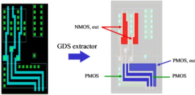
Required information is directly extracted from layout files in GDS format and mainly includes areas and positions of the active layer. The representative 3D struc-ture for Monte-Carlo simulation only contains N and P active junctions (drains and sources) of the design. The global collection volume takes into account the depletion capacitance of Drain and Source-Substrate junction. Fig. 8 illustrates the GDS extrac-tor applied to a NAND cell (0.35-µm technology). The GDS extracextrac-tor allows deduc-ing from the GDS file, the STI, the well locations and all active junctions.
Fig. 8. GDS extractor applied to academic NAND cell
Transient currents issued from physical model can be injected on each collection node, i.e., the drain of each transistor. Doing so, the electrical model of the transient pulses can be associated with the circuit netlist. The link between the layout and the netlist is performed in our flow thanks to the "Calibre" tool [13].
5.2 Electrical -level
Transient currents issued from physical model can be injected on each illuminated collection node (transistor drains or sources). Doing so, the electrical model of the transient pulses can be associated with the circuit netlist. The link between the layout and the netlist is performed in our flow thanks to the "Calibre" tool from Mentor
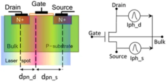
Graphics. According to this physical-level model, the laser effect is modeled at elec-trical level as a plug-in current source for each illuminated junction. The model is depicted in Fig. 9.
Fig. 9. Simple electrical model for a large spot laser-induced fault
In order to link the physical-level models and the electrical-level models for simula-tion purpose, a database was developed; each file corresponds to a standard cell in a given library and to a laser configuration data (energy, spot size). In each file, the transient current pulses I(t) are enumerated for each collection zone according to the position of the laser (dpn_d, dpn_s) for each logic state of the standard cell.
5.3 Logical level
The eventual effect of a current injection at electrical level in a digital circuit is a modified logic signal during a period of time related to the exposure time, the so-called transient fault. The propagation of the fault and the final consequences on the circuit behavior can then be analyzed using logic-level simulations. A multi-level fault simulator has therefore been implemented and will be described in section 6.
5.4 Behavioral Level
Finding design flaws late in the design flow is costly and strongly impairs the global development time. Evaluating the resilience of a given architecture at early design steps is therefore suitable. In most cases, such evaluations start at Register-Transfer Level (RTL) in order to benefit from a precise view of the registers in the design; higher-level descriptions are too abstract to clearly identify the real hardware that will be implemented in the circuit.
Early identification of design flaws can be achieved by using fault injection tech-niques [14]. At that level, the final design structure is not known so only errors in registers can be injected. The evaluation is meaningful only if errors injected at design time are actually representative of errors induced during a real attack. Also, evalua-tion time is limited so it is mandatory to trigger fault injecevalua-tion campaigns on reduced but significant sets of errors, including single-bit and multiple-bit error models.
Single-bit Errors.
A very usual assumption consists in modeling the effect of laser shots as bit-flips. However, some previous work reported that bit-flips are not necessarily an adequate model.
Previous work [15] has shown that, at least in some experimental conditions, er-rors are unidirectional. Bits are in that case always modified in the same manner, setting them to either zero or one. Such effects lead to the error models called bit-reset or bit-set. It means that more or less bits will be sensitive to the perturbation, depend-ing on the current state durdepend-ing the attack. The choice of the model may therefore have an impact on the resilience evaluation. Part of our work therefore aimed at identifying the impact of a given error model on the accuracy of early security evaluations w.r.t. differential fault attacks.
Fault injection experiments were defined on the basis of a simple circuit example, implementing a 16-bit sequential integer multiplier. This circuit is part of those cur-rently manufactured in 28nm technologies within the project LIESSE, and will be used in further work to compare in details early analyses with the consequences of real laser attacks. No error detection or tolerance mechanism is implemented in this circuit. Errors can therefore either be silent, or lead to computation errors (or crashes). The external communication protocol is based on handshake so the differences in computation time are not taken into account for the classification; only the result val-ue is checked. Crashes were very few so they will not be explicitly discussed.
Exhaustive single-bit error injections have been performed (in all flip-flops, at each clock-cycle, so a total of 11,410 injections) using the functional test bench used for validation of the circuit, then several similar test benches with random multiplica-tion operands.
The first outcome is clearly the impact of the circuit state on the difference in the percentage of computation errors for the 3 models (bit-flip, bit-set, bit-reset). For this particular example with the validation test bench, bits are more often at zero than one so the bit-reset model leads to noticeably more "non-injected" errors, i.e. injections that do not modify the flip-flop contents. About 3500 single-bit error injections have no impact for the set model, while near 8000 injections have no impact for the bit-reset model.
The second outcome is related to the use of the fault injection results. Considering the total number of injected errors, bit-flips are the most critical errors with 40.1% computation errors, while the bit-reset model only leads to 5.9% computation errors and the bit-set model leads to 34.3% computation errors. However considering only the actual bit modifications obtained during the campaign, the most critical injections correspond to bits forced at one, with 49.5% computation errors in that case (while the percentage is 19.6% for bits forced at zero).
When using random multiplication operands, the percentages are different, but the qualitative comparison of the three models is the same.
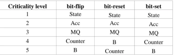
Table 1 illustrates a more detailed view, analyzing each register independently. The register criticality level is obtained with respect to the percentage of computation errors recorded after an exhaustive fault injection campaign with each of the error models. The percentage of computation errors noticeably differs from one model to
the other. However, the classification in terms of criticality only slightly differs for the functional test bench. In all cases the state register (storing the current state of the Finite State Machine) is the most critical. After that, two groups of registers can be identified (Acc/MQ and Counter/B) with some inversions between set and bit-reset. With random operands, results are similar for bit-flip and bit-reset, but slightly different for bit-set since the counter becomes the most critical register when "non-injected" errors are not considered.
Table 1. Classification of Internal Register Criticality for Single-bit Error Injections (Excluding
"Non injected" Errors) – Multiplier, Functional Validation Testbench
Criticality level bit-flip bit-reset bit-set
1 State State State
2 Acc Acc Acc
3 MQ MQ MQ
4 Counter B Counter
5 B Counter B
The choice of the right model to select for early fault injections therefore depends a lot on the designer intents. The bit-flip model creates more actual errors in the cir-cuit but is more independent of the application characteristics. If those characteristics have to be taken into account, and if experiments have shown the feasibility of bit-set or bit-reset errors for a given technology, those models may lead to more accurate results, with in some cases significant differences in the error percentages. If the goal is to identify the most critical registers, the three models may lead to very similar results, at least for our case study, and in that case the bit-flip model may lead to more efficient fault injection campaigns.
Multiple-bit Errors.
One of the key benefits of a laser source, as a tool to perform fault-based attacks, is its high precision locality, although a single laser shot may generate either single or multiple faults inside an integrated circuit. These characteristics must be taken into account by an RTL laser fault model assuming multiple-bit errors. Usual methods based only on fault injections for a given maximum error multiplicity are quite time-consuming and do not take into account the locality characteristics. Although at RT-Level it is not possible to precisely know the final placement of the element, it is pos-sible to evaluate proximity on the basis of functional relationships.
There are two different categories of faults that can finally affect the circuit and potentially create an error. A fault may originate either from the combinational part or it can be directly injected inside a flip-flop (FF). Our proposed approach is attempting to unify these two different ways of introducing faults by modeling faults injected into the FFs of the design.
Our approach, as described in [16], makes use of a logic cone partitioning meth-odology, capable of introducing the notion of locality to an early RTL analysis includ-ing the ability to model multiple faults. The developed tool uses the elaborated RTL
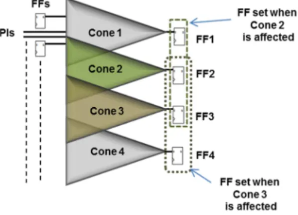
netlist of a behavioral (VHDL) description. The elaborated netlist and its analysis are obtained thanks to the Verific front-end API [17]. As shown in Fig. 10, the circuit under analysis is partitioned into intersecting functional blocks of combinational log-ic, called logic cones. Each cone starts from FFs of the circuit and/or primary inputs, and ends to another FF and/or a primary output.
Fig. 10. Logic cone partitioning of the elaborated netlist
Given a subset of the circuit, assumed as the area under attack, we are thus able to determine the sequential elements that may potentially contain an error.
Initially each attack is assumed to impact an entire logic cone and the application generates for each cone under attack a set of FFs that may potentially capture a fault. In a second step, depending on the results, this assumption can be modified to better focus laser attacks in suppressing some logic dependencies. Since we are able to know the functional relationship between the FFs of the design, we can also deduce information about the FFs that are likely to be attacked concurrently by a single laser shot, because of their potentially adjacent placement later in the design flow.
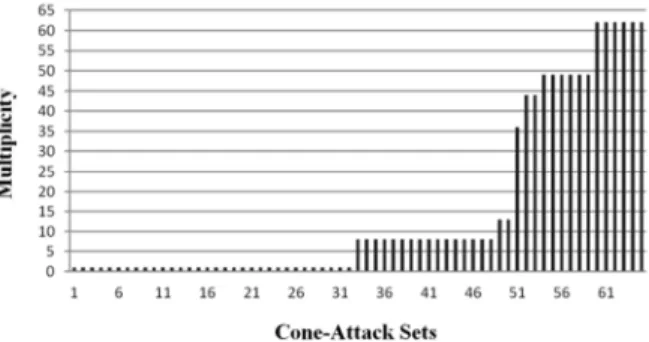
The method leads to the creation of a fault space with varying multiplicities for each attack depending on the functional relationship between the cone under attack and all the remaining cones of the circuit [18]. For example in Fig. 11, when Cone 2 is under attack, its fault set includes FFs: 1, 2 and 3; when Cone 3 is affected, the corresponding set includes FFs: 2, 3 and 4. These sets are also referred to as "cone-attack sets".
Then, multiple-bit errors are injected into each cone-attack set. Our results show that the approach achieves a noticeable reduction of the size of the fault space, compared to random exhaustive multi-bit fault approaches, without even considering a maxi-mum multiplicity for each attack. This way we can save computational resources for a fault injection campaign and, at the same time, take into account faults that are more realistic when we model a localized laser attack. Errors are injected into the FFs of the design so the approach is compatible with fast emulation techniques that can be very useful for an RTL evaluation.
As an example, Fig. 12 shows the sets obtained for the 128-bit datapath of an AES crypto-processor. The largest cone-attack sets include 62 FFs so errors with a maxi-mum multiplicity of 62 may be injected for those sets. On the opposite, for all sets with only one FF, single-bit error injections are sufficient. In the classical approach, the maximum multiplicity would be defined more arbitrarily and errors would be injected randomly in the global set of 512 FFs.
Fig. 12. Size of AES data path cone-attack sets
6
CAD Tools
The proposed security-evaluation flow is supported by several tools dealing with dif-ferent abstraction levels. First, the databases of induced currents is generated using the MUSCA SEP3 tool on every standard cell, then the Calibre tool is used to transfer this information on the netlist of the circuit under evaluation as presented in section 5.1 and 5.2.
Developed on the basis of the 0-delay simulator LIFTING [19], tLIFTING (timing LIFTING) [20] is an open-source fault simulator for single/multiple stuck-at faults, single/multiple upsets and single/multiple transients faults. The tool allows 0-delay/delay-annotated logic-level simulations and transistor-level fault simulation for digital circuit described in Verilog. Cooperating with a set of sub-tools, this simulator is able to perform transistor-level simulations based on the laser-induced fault model (current curves) and then further logic-level simulation for the whole circuit in order to analyze propagations of transient misbehaviors. As an open-source tool, it was expanded to read the database generated by MUSCA SEP3. Fig. 13 shows how these tools interact with each other to produce simulation reports of laser-induced faults.
The simulation process is illustrated in Fig. 14: starting from the laser’s parame-ters (size, position, power) and circuit layout information, affected PN junctions are located as sub-circuit in the design, and corresponding I(t) curves are extracted from the database. The corresponding electrical fault models are injected into the affected sub-circuit at transistor-level description. Then the whole system is simulated at logic-level in order to compute the sub-circuit input waveforms during the whole external perturbation. This information is then provided to the electrical-level simulator in charge of the simulation of the sub-circuit in order to simulate the electrical perturba-tion. After electrical simulation of the affected gates, if the perturbation changes the state of circuit nodes, these new values are translated to logic-level for finishing the fault simulation at logic-level.
Fig. 13. From physical-level to logic-level laser-induced faults simulation
At higher level, prototyping platforms are used in order to evaluate early in the design flow the functional consequences of errors. These platforms are based on commercial FPGA development boards, but specific tools have been developed in order to man-age the injection process. Platform examples are cited in [21].
7
Counter-Measures
Several types of hardware counter-measures are developed in order to improve the circuit resilience to laser-based attacks. The existing counter-measures can be classi-fied as technological counter-measures (such as metal shield), redundancy-based measures for error detection (e.g. [22][23][24]), detector-based counter-measures which focus on fault detection (e.g. [25][26]). In this chapter, we detail a counter-measure based on laser beam detection, i.e. a detector-based approach. The principle consists in designing a cell with higher sensibility to laser attack than any other cell in the library, and then to spread several instances of that cell over the de-vice in order to trigger an alarm wherever the laser beam hits the circuit.
7.1 Structure of the Detector
We choose an inverter as detector because of its small size compared to other cells. When both its NMOS and PMOS transistors are affected by a laser spot, the ampli-tude of the transient current pulse Iph_out on the inverter output is the difference between the photocurrents generated in both transistors: Iph_out = Iph_dp - Iph_dn (Fig. 15(left)). When the inverter input is set to 1, transistor PMOS is OFF, transistor NMOS is ON, a positive current pulse Iph_out can be observed at the cell’s output due to the laser attack. When Iph_out is large enough, the inverter output switches temporary from 0, the fault-free state, to 1, and this transition can be used to propa-gate an alarm signal (laser attack detection).
In order to improve the detection of a laser shot thanks to such inverter-based light sensor, and make the sensor more sensible than any other gate in the design, we must increase Iph_out on the sensor output. We thus propose to design a new inverter from the regular INV2 cell of the working library (AMS C35 technology) such that Iph_dp increases, Iph_dn decreases, and thus Iph_out increases.
Fig. 15. (left) Laser-induced effect in an inverter, and (right) Inverter-based detector cell
For that, we combined a large PMOS transistor with a small NMOS one. We designed a new cell from these two transistors, the S_INVP3 inverter shown in Fig. 15 (right). The ratio of the P+/N- and N+/P- junction areas in this new cell is now 48:5 instead of 8:5 as in the original standard inverter INV2 of the target library. As detailed in [27] for logic gates, and in [7] for SRAM cells, the photocurrents Iph_dp and Iph_dn being proportional to the area of the junctions, this new area ratio between the inverter’s PMOS and NMOS transistors allows us to increase Iph_dp compared to Iph_dn and thus to increase Iph_out. The proposed invertor-based sensor is thus more sensible than the original cells (see Fig. 16 for comparison between several cells).
Similarly, we elaborated another sensor named S_INVN3 for which the ratio of the P+/N-well area and N+/P-sub is 8:30. Conversely to the S_INVP3 detector, the S_INVN3 input must be set 0 (P transistor ON, N transistor OFF) so that a laser beam provokes a negative pulse on the detector output that switches temporary from 1 (fault-free state) to 0 (transient fault used to detect the laser attack). Since detector cells have the same height as other standard cells, they can be easily integrated into the design.
7.2 Detector Sensitivity
Fig. 16 shows for several cells the minimum current density required for different laser pulse duration in order to temporarily switch the cell output. These results were obtained from models and tools developed in the framework of the LIESSE project.
Fig. 16. Minimum current density for transmissible or detectable transient pulse (mA/µm2)
Clearly, the two proposed detectors are more sensitive to laser illumination than other standard cells thanks to the proposed (over)sizing of the PMOS (resp. NMOS) net-work compare to the NMOS (resp. PMOS) netnet-work in the proposed S_INVP3 (resp. S_INVN3) sensor. On average, the S_INVP3 is 6.5 times more sensitive than a NAND2 gate with input values set to "10", and 18.9 times more sensitive than this NAND2 gate when its input values are set to "11". For S_INVN3, these ratios are 5.1:1 and 15.1:1.
7.3 Insertion of detectors in the design
The principle is to spread detectors in the layout such that any spot location is detect-ed by one or several detectors, and the detection signal is not maskdetect-ed by other detec-tors. For gathering all detector signals to a single detection flag, the detectors are combined into a chain-based structure as shown in Fig. 17. In this example, 4 chains have been built and connected to the flag FF thanks to a NOR gate.
Fig. 17. The detector chain structure for injected fault detection
As an example, when this detector-based countermeasure is applied for protecting a substitution-box of an AES co-processor, the area overhead is of 4.17% of the original substitution-box. We performed 2000 laser-induced-fault simulations on that exam-ple. In each experiment, the location of the laser spot and the circuit input patterns was randomly chosen. The laser spot diameter was assumed to be 40µm, i.e. covering 20 standard cells, and the current density was set to 0.08mA/µ m2. From these simula-tions we obtained 3.1% of error rate on the substitution-box and 100% of detection rate (non-detected error: 0%) thanks to the extra INV-based detectors.
8
Conclusions
This paper summarizes the main results obtained so far in the LIESSE project. Work is on-going to refine the tools and compare their outcomes with actual attacks on bulk and FDSOI prototypes.
FDSOI is often introduced as a technological answer to radiation effects and also to laser-based fault attacks [8, 28] due to the thin box that isolates the CMOS transis-tors from their wells. To date, an experimental validation of these expectations is still pending. We brought to the reader attention the first results we have obtained on iso-lated NMOS transistors (at 28nm technology node) that tend toward proving this as-sumption. The magnitude of the laser-induced photocurrents in FDSOI transistors was found significantly lower than that induced in bulk transistors. However, we also find out that the effect area of a laser spot is reduced for FDSOI. This may be worrying because it may help an attacker to restrict fault injection to a few bits, thus making it easier to fulfill the fault models required for differential fault attacks [29]. However, these first results and assumptions must be corroborated on ICs at the state-of-art
complexity: our next research work will be to compare the laser-fault sensitivity of two CMOS 28nm circuits embedding a hardware implementation of the AES crypto-algorithm respectively in FDSOI and bulk technologies. If full immunity seems out of scope, we nonetheless expect a reduced laser sensitivity of the FDSOI devices.
Models and tools are now available for simulation of laser-silicon interactions from low levels, for better precision on the interaction, to high levels, for dealing with large devices.
A laser-induced transient pulse model was proposed at physical level including the laser interaction in Silicon step, the carrier transport and charge collection mecha-nisms. This physical model calculates the transient-current response based on the underlying physics phenomena (field modulation, multiple-node charge, diffusion) and laser characteristics as the wavelength, the energy, the focalization properties and the size beam. A GDS extraction process allows for identifying the collection area in the circuit design, and transient-currents issued from physical model can be injected at circuit level. The first results on isolated N and PMOS transistors at 28nm technology node were obtained. Transient-current characteristics were compared for modelling and experiment results (as function of laser properties), first results are satisfactory. The short-term perspectives will be to use the physical model for FDSOI and bulk technologies on more complex circuits.
Results obtained on RT-level fault injections based on emulation show that the choice of the error model has noticeable effects on the early predictions made at de-sign time. Bit-flip injections lead to more injected errors, but bit-set or bit-reset injec-tions can have more impact when effective. The choice of the model therefore de-pends on the injection campaign objectives (qualitative or quantitative) and also on the knowledge of the technology and on the application execution, leading to more or less 0's and 1's in registers. Laser-based experiments on the LIESSE demonstrators will allow to better decide about the model to select.
For designers, performing fault effect analysis early in the design flow is a must. This early analysis can avoid time consuming and very expensive design re-spins. We thus propose a way to extract security-related information from RTL descriptions, particularly a list of Flip-Flop sets potentially affected at the same time by a laser shot according to the laser locality characteristics. This high-level fault injection approach is more realistic than the usual random multi-bit fault injection approach used in the literature. However our approach assumes that each laser spot impacts concurrently one entire single RTL cone and, therefore, all its intersecting cones. In our next work we will show the extent of the validity of this assumption by comparing the sets of Flip-Flops extracted from the RTL circuit description, and supposedly affected by the same laser shot, with the Flip-Flop sets arising from local attacks on the finalized layout of a circuit.
Acknowledgment.
This work has been supported by the French National Research Agency project "LIESSE" (ANR-2012-INSE-0008). The counter-measure development has also been partially supported by the contract FUI CALISSON 2 (DGCIS AAP10). TIMA is Partner of the Labex PERSYVAL Lab (ANR-11-LABX-0025).
We would like to thank Verific Design Automation Inc. for providing the Sys-temVerilog and VHDL front-end used for the implementation of our RTL methodolo-gy.
References
1. R. Leveugle, P. Maistri, P. Vanhauwaert, F. Lu, G. Di Natale, M.-L. Flottes, B. Rouzeyre, , A. Papadimitriou, D. Hely, V. Beroulle, G. Hubert, S. De Castro, J.-M. Dutertre, A. Sarafianos, N. Boher, M. Lisart, J. Damiens, P. Candelier, C. Tavernier., "Laser-induced Fault Effects in Security-dedicated Circuits", IEEE 22nd International Conference on Very Large Scale Integration, VLSI-SoC’14, 2014, DOI: 10.1109/VLSI-SoC.2014.7004184. 2. S. P. Skorobogatov and R. J. Anderson, "Optical fault induction attacks," 4th International
Workshop on Cryptographic Hardware and Embedded Systems, CHES ’02, pp. 2–12, Springer-Verlag, 2002.
3. J.M. Dutertre, S. De Castro, A. Sarafianos, N. Boher, B. Rouzeyre, M. Lisart, J. Damiens, P. Candelier, M.L. Flottes, D. Di Natale. Design & Technology of Integrated Systmes in Nanoscale Era. DTIS 2014
4. R. C. Baumann, "Radiation induced soft errors in advanced semiconductor technologies," Device and Materials Reliability, IEEE Transactions on, 2005. 5(3): pp. 305-316.
5. G. C. Messenger, “Collection of Charge on Junction Nodes from Ion Tracks”, IEEE Trans. Nuclear Science, vol. 29, no. 6, pp. 2024–2031, 1982.
6. V. Carreno, G. Choi, and R. K. Iyer, “Analog-digital simulation of transient-induced logic errors and upset susceptibility of an advanced control system”, in NASA Technical Memo 4241, 1990.
7. A. Sarafianos, C. Roscian, J.-M. Dutertre, M. Lisart, A. Tria, "Electrical modeling of the photoelectric effect induced by a pulsed laser applied to an SRAM cell," Microelectronics Reliability, vol. 53, no. 9-11, pp. 1300-1305, 2013.
8. D. Golanski et al., "First demonstration of a full 28nm high-k/metal gate circuit transfer from bulk to utbb fdsoi technology through hybrid integration," Symposium on VLSI Technology (VLSIT), 2013, pp. T124-T125, June 2013
9. V. Ferlet-Cavrois et al., "Direct measurement of transient pulses induced by laser and heavy ion irradiation in deca-nanometer devices," IEEE Transactions on Nuclear Science, vol. 52, pp. 2104-2113, December 2005.
10. A. Sarafianos, R. Llido, J.-M. Dutertre, O. Gagliano, V. Serradeil, M. Lisart, V. Goubier, A. Tria, V. Pouget, and D. Lewis. "Building the electrical model of the Photoelectric Laser Stimulation of a NMOS transistor in 90 nm technology", Conference Proceedings from the 38th International Symposium for Testing and Failure Analysis, Phoenix, États-Unis, 2012.
11. G. Hubert, L. Artola, "Single-Event Transient Modeling in a 65 nm Bulk CMOS Technol-ogy based-on Multi-Physical Approach and Electrical Simulations," IEEE Transactions on Nuclear Science, vol. 60, no.6, Dec. 2013.
12. P.E.Schmid, Optical Absorption in Heavily Doped Silicon, Phys. Review B, vol. 23, 1981, pp. 5531-5536.
13. http://www.mentor.com/
14. R. Leveugle, "Early analysis of fault-based attack effects in secure circuits," IEEE Trans-actions on Computers, vol. 56, no. 10, pp. 1431-1434, October 2007.
15. C. Roscian, J.-M. Dutertre, A. Tria, "Frontside laser fault injection on cryptosystems - Ap-plication to the AES' last round," International Symposium on Hardware-Oriented Security and Trust (HOST) , pp. 119-124, 2013.
16. A. Papadimitriou et al., "A multiple fault injection methodology based on cone partitioning towards RTL modeling of laser attacks," Design, Automation and Test in Europe Confer-ence (DATE), March 24-28, 2014.
17. www.verific.com
18. P. Vanhauwaert et al., "On error models for RTL security evaluations," International Con-ference on Design & Technology of Integrated Systems in Nanoscale Era" (DTIS), 2014. 19. A. Bosio, G. Di Natale, “LIFTING: A Flexible Open-Source Fault Simulator”, 17th Asian
Test Symposium, Sapporo, Nov. 2008, pp. 35 - 40.
20. F. Lu, G. Di Natale, M.-L. Flottes, B. Rouzeyre, "Laser-Induced Fault Simulation," DSD, pp. 609-614, 2013.
21. M. Ben Jrad, R. Leveugle, "Comparison of FPGA platforms for emulation-based fault in-jections using run-time reconfiguration," 27th Conference on Design of Circuits and Inte-grated Systems (DCIS), pp. 184-188, November 28-30, 2012.
22. S. Moore, R. Anderson, P. Cunningham, R. Mullins, G. Taylor, “Improving Smart Card Security Using Self-Timed Circuits”, In Proceedings of the Eighth International Symposi-um on Asynchronous Circuits and Systems, Manchester, UK, 9-11 April 2002, pp. 211-218.
23. J. Rajendran, H. Borad, S. Mantravadi, R. Karri, “SLICED: Slidebased Concurrent Error Detection Technique for Symmetric Block Ciphers”, Hardware-Oriented Security and Trust (HOST), 2010 IEEE International Symposium on, pp. 70-75.
24. G. Di Natale, M. Doulcier, M.-L. Flottes, B. Rouzeyre, “A Reliable Architecture for Paral-lel Implementations of the Advanced Encryption Standard”, Journal of Electronic Testing (JETTA), Springer, Volume 25 Issue 4-5, August 2009, pp. 269-278, DOI: 10.1007/s10836-009-5106-6.
25. R. P. Bastos, F. S. Torres, J.-M. Dutertre, M.-L. Flottes, G. Di Natale, B. Rouzeyre, “A bulk built-in sensor for detection of fault attacks”, , 2013 IEEE International Symposium on Hardware-Oriented Security and Trust (HOST), pp. 51-54.
26. M. Lisart, A. Sarafianos, O. Gagliano, M. Mantelli, “Device for protecting an integrated circuit chip against attacks”, publication N°: FR2976722, Dec 2012.
27. L. Feng, G. Di Natale, M.-L. Flottes, B. Rouzeyre, “Customized Cell Detector for Laser-Induced-Fault Detection”, IEEE 20th International On-Line Testing Symposium (IOLTS’14), 2014, pp. 37-42. DOI: 10.1109/IOLTS.2014.6873669.
28. M. Alles, R. Schrimpf, R. Reed, L. Massengill, R. Weller, M. Menden- hall, D. Ball, K. Warren, T. Loveless, J. Kauppila, and B. Sierawski, “Radiation hardness of fdsoi and fin-fet technologies,” 2011 IEEE International in SOI Conference (SOI), pp. 1–2, Oct 2011. 29. A. Barenghi, L. Breveglieri, I. Koren, and D. Naccache. “Fault injection attacks on
crypto-graphic devices: Theory, practice, and countermeasures”. Proceedings of the IEEE, 100:3056 – 3076, 2012.
![Fig. 1. The mechanism responsible for Optical Beam Induced Current [3]](https://thumb-eu.123doks.com/thumbv2/123doknet/13535592.418223/3.892.324.564.708.812/fig-mechanism-responsible-optical-beam-induced-current.webp)
![Fig. 2. Typical shape of nodal current at a p-n junction [4]](https://thumb-eu.123doks.com/thumbv2/123doknet/13535592.418223/4.892.358.537.224.355/fig-typical-shape-nodal-current-p-n-junction.webp)
![Fig. 7. Laser induced photocurrent magnitude [µA] in the drain diffusion of transistors #1 and](https://thumb-eu.123doks.com/thumbv2/123doknet/13535592.418223/8.892.203.691.474.747/fig-laser-induced-photocurrent-magnitude-drain-diffusion-transistors.webp)