Publisher’s version / Version de l'éditeur:
Nano Letters, 14, 7, pp. 4102-4106, 2014-06-13
READ THESE TERMS AND CONDITIONS CAREFULLY BEFORE USING THIS WEBSITE.
https://nrc-publications.canada.ca/eng/copyright
Vous avez des questions? Nous pouvons vous aider. Pour communiquer directement avec un auteur, consultez la
première page de la revue dans laquelle son article a été publié afin de trouver ses coordonnées. Si vous n’arrivez pas à les repérer, communiquez avec nous à PublicationsArchive-ArchivesPublications@nrc-cnrc.gc.ca.
Questions? Contact the NRC Publications Archive team at
PublicationsArchive-ArchivesPublications@nrc-cnrc.gc.ca. If you wish to email the authors directly, please see the first page of the publication for their contact information.
NRC Publications Archive
Archives des publications du CNRC
This publication could be one of several versions: author’s original, accepted manuscript or the publisher’s version. / La version de cette publication peut être l’une des suivantes : la version prépublication de l’auteur, la version acceptée du manuscrit ou la version de l’éditeur.
For the publisher’s version, please access the DOI link below./ Pour consulter la version de l’éditeur, utilisez le lien DOI ci-dessous.
https://doi.org/10.1021/nl501648f
Access and use of this website and the material on it are subject to the Terms and Conditions set forth at
Nanowire waveguides launching single photons in a Gaussian mode
for ideal fiber coupling
Bulgarini, Gabriele; Reimer, Michael E.; Bouwes Bavinck, Maaike; Jöns,
Klaus D.; Dalacu, Dan; Poole, Philip J.; Bakkers, Erik P. A. M.; Zwiller, Val
https://publications-cnrc.canada.ca/fra/droits
L’accès à ce site Web et l’utilisation de son contenu sont assujettis aux conditions présentées dans le site LISEZ CES CONDITIONS ATTENTIVEMENT AVANT D’UTILISER CE SITE WEB.
NRC Publications Record / Notice d'Archives des publications de CNRC:
https://nrc-publications.canada.ca/eng/view/object/?id=b8bb4646-d6fd-43e7-aaa1-e72cec4ef898 https://publications-cnrc.canada.ca/fra/voir/objet/?id=b8bb4646-d6fd-43e7-aaa1-e72cec4ef898
Nanowire Waveguides Launching Single Photons in a Gaussian
Mode for Ideal Fiber Coupling
Gabriele Bulgarini,*
,†Michael E. Reimer,
†Maaike Bouwes Bavinck,
†Klaus D. Jöns,
†Dan Dalacu,
‡Philip J. Poole,
‡Erik P. A. M. Bakkers,
†,§and Val Zwiller
††
Kavli Institute of Nanoscience, Delft University of Technology, 2628 CJ Delft, The Netherlands
‡
National Research Council of Canada, K1A 0R6 Ottawa, Canada
§
Eindhoven University of Technology, 5612 MB Eindhoven, The Netherlands
ABSTRACT: Quantum communication as well as integrated photonic circuits require single photons propagating in a well-defined Gaussian mode. However, tailoring the emission mode to a Gaussian remains an unsolved challenge for solid-state quantum emitters due to their random positioning in the host material or photonic structure. Here, we overcome these limitations by embedding a semiconductor quantum dot in a tapered nanowire waveguide. Owing to the deterministic positioning of the emitter in the waveguide, we demonstrate a Gaussian emission profile in the far field. Hence, we further couple the emission into a single-mode optical fiber with a record efficiency of 93%, thereby addressing a major hurdle for practical implementation of single photon sources in emerging photonic technologies.
KEYWORDS: Quantum dot, nanowire, single photon emission, waveguide modes, Fourier microscopy
T
he most established method to date in order to achieve a very bright single-photon source using nanowires is by coupling the quantum dot emission to the fundamental waveguide mode and to shape the tip of the nanowire for efficiently directing the single photons toward the collection optics.1−3 Two alternative routes have been experimentally realized for out-coupling of the light. The first strategy is to shape the nanowire tip with a narrow taper.4This narrow taper gradually transfers the guided mode from inside the nanowire waveguide to outside, thus avoiding reflections at the semiconductor−air interface. The expanded mode also reduces the far field emission angle, which enables efficient light collection with limited numerical aperture optics. This gradual transfer of the light from the guided mode to the far field exhibits the best performance at very small tapering angles,5i.e., the transmission is approximately 100% for angles smaller than 2°. These very small angles are currently state-of-the-art and are only achievable by growing the nanowire structure with bottom-up techniques.2 Alternatively, the nanowire can be shaped with a trumpet-like microstructure with the base being smaller than the tip.6 In this case, the guided mode expands inside the waveguide before being transmitted to the far field. Both approaches promise a Gaussian emission profile, which is ideal for coupling to single-mode fibers for long distance communication. In this work, we measure the photo-luminescence intensity of individual quantum dots in tapered nanowire waveguides in the Fourier space. An excellent overlap of the emission with a Gaussian profile is first imaged with Fourier spectroscopy and subsequently demonstrated bycoupling single photons to a single-mode fiber with negligible insertion losses.
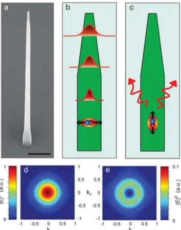
The scanning electron micrograph of Figure 1a presents our system: a bottom-up grown InP nanowire, with an ultrasmooth tapered tip (1°), containing a single InAsP quantum dot. Typical nanowire length of the investigated nanowires is 5 ± 2 μm. Importantly, the site-selective growth with only one quantum dot per nanowire waveguide allows us to select single emitters and image their emission profile down to the single exciton level. Details on the precise positioning of the quantum dot and the bottom-up growth technique can be found elsewhere.2,7,8
We first investigate the spatial distribution of the quantum dot emission in the far field depending on the dipole orientation associated with the ground state exciton transition. We model a single exciton confined in the quantum dot as an electrical dipole positioned exactly on the nanowire axis and calculate numerically the emission profile propagating upward from the nanowire tip in the far field using finite difference time domain (FDTD) simulations. The near field solutions of the electromagnetic field are decomposed and projected to the far field by a set of plane waves propagating at different angles. The projection functions yield the electromagnetic field distribution on a plane positioned in the far field as a function of the
Received: May 2, 2014
Revised: June 5, 2014
Published: June 13, 2014
emission angle or k vector. We use nanowire dimensions that correspond to the experimentally investigated ones: diameter, D = 200 nm, 1° taper at the tip, and emission wavelength λ = 950 nm. The refractive index of InP at 950 nm is 3.37 and the dispersion relations used in the simulations are obtained from ref 9. As observed in Figure 1a, the gold droplet of 20 nm in diameter, which has catalyzed the nanowire growth, is found at the tip of the nanowire. Because of the nanometric thickness and the negligible area compared to the guided mode, the gold droplet is omitted from the calculations. We consider two orthogonal orientations of the dipole: perpendicular (Figure 1b) or parallel (Figure 1c) to the nanowire axis. The direction of the electrical dipole is shown schematically in Figure 1b,c as a double sided arrow. In Figure 1d,e we present the calculated electric field intensity of the far field at the top of the nanowire for the configurations displayed in Figure 1b,c, respectively.
When the quantum dot dipole is oriented perpendicular to the nanowire axis (Figure 1d), an excellent coupling (β > 95%) of the quantum dot emission to the fundamental waveguide mode is achieved.10 At optimum waveguide conditions, the quantum dot emission is guided along the nanowire, adiabati-cally transferred to the far field and the larger fraction of this light is collected at small angles. In contrast, the emission of a dipole oriented along the nanowire axis couples very poorly to
the fundamental waveguide mode. In this latter case, the emission propagates through nonguided leaky channels, resulting in an emission pattern having a minimum intensity at k∥= (kx2+ ky2)1/2= 0 and maximum intensity for k∥= 0.34
(which corresponds to an angle of ∼20° with the nanowire axis), as shown in Figure 1e. Moreover, because of this weak coupling to guided modes, the integrated electric field intensity in the far field is 11 times lower for the parallel dipole configuration as compared to a perpendicular dipole, which is in agreement with the inhibition of the spontaneous emission that is observed for suppressed waveguide conditions.7,11
In Figure 2 we present the far field emission profile of a single quantum dot in a tapered nanowire waveguide obtained
by Fourier imaging. The emission spectrum of the quantum dot at 5 K is displayed in Figure 2a. A single peak is observed that is attributed to the recombination of a single exciton in the quantum dot s-shell. We verify the single photon statistics with the correlation measurement shown in the inset.
Operation of the Fourier microscopy technique used to measure the single quantum dot angular emission distribution is explained in the schematics of Figure 2b. The quantum dot emission is collected with a high numerical aperture (NA = 0.8) objective with the emitter positioned at the objective focus. As a consequence, the Fourier-plane information on the emitter is obtained at the back-focal plane of the objective,12−15where the angular distribution of collected photons is set by their k-vector in the reciprocal space. In order to measure the light intensity distribution in the Fourier-space of the quantum dot, we image the back-focal plane of the objective onto a CCD forming a so-called Fourier image.
We position a lens of focal distance f in the middle of the objective and CCD camera as displayed in Figure 2b. Thus, the back-focal plane of the objective is reproduced onto the CCD
Figure 1. Tapered nanowire waveguide. (a) Scanning electron micrograph of a nanowire waveguide containing a single quantum dot on its axis. Nanowire diameter ∼200 nm, tapering angle ∼1°. Scale bar is 0.5 μm. (b,c) Schematics of waveguide containing a perpendicular (b) or parallel (c) dipole used for FDTD simulations of the emission profile in the far field. Results are shown in the lower panel for (d) perpendicular and (e) parallel dipole. The intensity of the electric field, E, is normalized to the maximum intensity of panel d for both simulations. kx and ky indicate the momentum in a plane
perpendicular to the nanowire axis.
Figure 2. Fourier imaging of single quantum emitter. (a) Typical photoluminescence spectrum of a single quantum dot in a nanowire waveguide well-below exciton saturation. Inset shows typical antibunching of the second order intensity correlation function for the single exciton line (green) and fit to the data (yellow, g(2)(0) =
0.05). (b) Schematics of the Fourier microscopy setup. An image of the objectve back-focal plane, containing the Fourier-space informa-tion on the emitter, is acquired on a silicon CCD. (c) Far field emission profile measured via Fourier imaging from the spectrum in panel a. Most of the photoluminescence is collected around k = 0, which indicates a perpendicular orientation of the dipole with respect to the waveguide axis.
Nano Letters Letter
dx.doi.org/10.1021/nl501648f | Nano Lett. 2014, 14, 4102−4106
with a one to one image, thereby mapping the emission intensity as a function of k coordinates without altering the emission profile information via transmission through the optical setup. The black dashed lines indicate how the Fourier image is formed on the CCD by classic ray-optics description. The angular distribution of the single exciton photo-luminescence, presented in Figure 2a, is shown in the color plot of Figure 2c. The intensity of collected photoluminescence (PL) is mapped out in the Fourier-plane of the quantum emitter. We observe that most of the light is collected at small k, corresponding to a small angular distribution. This result is in excellent agreement with the numerical simulations presented in Figure 1d and confirms that the electrical dipole associated with a single exciton in the quantum dot is oriented perpendicular to the nanowire axis. We note here that measuring a single quantum emitter in the Fourier space is a technical challenge, which is overcome with two crucial ingredients. First, the brightness of the source, which is described in our previous work,2 allows for a high count-rate per pixel to image the emission profile of a single quantum dot. Second, the site-selected growth technique that we employ allows for a single quantum dot per nanowire waveguide, and thus, only a single emitter is addressed with a nearly diffraction-limited laser spot. This latter feature is of special importance for Fourier imaging because in order to conserve the k-vector of the photons, no diffraction grating can be utilized for the spectral filtering of the emission lines.
Figure 3a (b) shows the measured (calculated) 3D far field emission profile of a single quantum dot in a tapered nanowire waveguide. The experimental results are in excellent agreement with the numerical calculations. Remarkably, the 3D plot evidence that the quantum dot emission profile in the far field is a Gaussian, with an overlap integral of 98.8 ± 0.1% with the guided mode of a single-mode fiber. The overlap is shown in Figure 3c, a 2D cut through the measured profile (blue) in spatial coordinates as compared to the mode of a single-mode fiber designed for 950 nm (mode field diameter of 5.6 μm). Typically, we observe an average overlap exceeding 97% on several nanowire waveguides operating in the single-mode regime, thus outperforming photonic crystal cavities.14,16 Compared to photonic crystals, nanowire waveguides have the additional advantage of having a single emitter per waveguide, which is deterministically coupled to the waveguide mode and thus the possibility of fabricating arrays of single photon emitters.
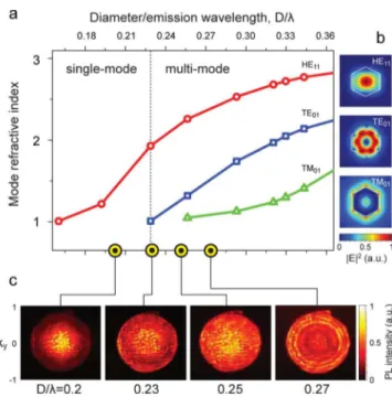
As a function of the nanowire diameter, more than one order of waveguide modes becomes allowed in the nanowire.17We now investigate the influence of the nanowire diameter on the
spatial profile of the emission in the far field. First, we calculate the available guided modes in the nanostructure. Figure 4a
shows a calculation of the effective refractive index for the first three guided modes as a function of the nanowire waveguide diameter, D, and the photon wavelength, λ. For diameters around 0.2λ, the nanowire is a single-mode waveguide since only propagation of the fundamental guided mode, HE11, is
supported. Note that the HE11mode comprises two orthogonal
components that in a circularly symmetric waveguide are degenerate. At a larger nanowire diameter, the nanowire becomes a multimode waveguide. We show the first two allowed higher order modes, namely, the TE01and TM01. The
intensity distribution of the electric field in the TE01and TM01 Figure 3.Near-unity Gaussian emission profile of single-mode nanowire waveguide. (a) Three-dimensional image of the emission profile for D/λ = 0.21. The intensity of the PL collected as a function of kxand kyis both color-coded and displayed on the z-axis. The emission profile has a Gaussian
shape and matches very well the calculated profile for a taper length of 1 μm, shown in panel b. (c) The overlap integral of the emission profile from panel a with the Gaussian mode of a single-mode fiber is 98.8 ± 0.1%. The excellent overlap is exhibited by a 2D cut through the measured profile from panel a, in blue color, compared with the guided mode in the fiber displayed in red.
Figure 4.Nanowire waveguide modes. (a) Confined guided modes in a nanowire waveguide at varying nanowire diameter. For D/λ below 0.23 the nanowire supports only a single guided mode (HE11) and
becomes a multimode waveguide for higher diameters. The first two higher order modes: TE01 and TM01 are shown. Calculations give
equal mode confinement using hexagonal or circular cross sections,17 for a side s of the hexagon such that 2s = 1.14 × D. The spatial distribution of the electric field of the modes inside the waveguide is shown in panel b. (c) Far field emission pattern of s-shell luminescence from for increasing waveguide diameters. The emission increasingly loses affinity with a Gaussian profile as the nanowire diameter is enlarged.
guided modes is displayed in Figure 4b for a nanowire cross-section of D/λ = 0.3.
In Figure 4c we plot four Fourier images obtained by collecting the s-shell photoluminescence of individual quantum dots located in nanowires with increasing diameters. We observe that as a function of the nanowire diameter, the coupling of the quantum dot emission to different waveguide modes modifies the far field emission pattern. When only the HE11 mode is supported by the nanowire waveguide (D/λ <
0.23), the far field emission is Gaussian. As the nanowire diameter is enlarged and the nanowire becomes a multimode waveguide, we observe an increase in PL collected at higher angles. The emission pattern flattens for D/λ = 0.25 and assumes a subtle doughnut profile at D/λ = 0.27. This deviation from Gaussian profile observed for large nanowire diameters is attributed to the coupling of the quantum dot emission to the TE01and TM01waveguide modes.
We finally illustrate the practicality in coupling the Gaussian emission from the tapered nanowire waveguide to a single-mode fiber. We couple the single photon emission into an antireflection coated optical fiber using a 5× Olympus long working distance plan achromat objective (NA of 0.1) with transmission optimized for the near-infrared wavelength range. In order to determine the coupling efficiency, we measure the single quantum dot PL intensity either with or bypassing the single-mode fiber coupling optics and detecting the photons on a CCD camera after filtering individual exciton lines with a high-resolution single grating spectrometer. The schematics of the experiment is shown in Figure 5a. The integrated PL count-rate that we observe via the fiber (red curve in Figure 5b) is 93 ± 3% of that measured by free-space propagation (blue spectrum). The efficiency is obtained from peak integrated counts averaged over multiple spectra and from two separate coupling attempts. This measured efficiency compares with 45% reported for self-assembled quantum dots in planar cavities18 and with 70% estimated for quantum dots in
micropillar cavities.19 Remarkably, the Gaussian profile provided by nanowire waveguides enables us for extending fiber-coupling efficiency toward unity within still remaining technological limitations of commercially available optical components.
We have measured the far field emission profile of individual quantum dots in tapered nanowire waveguides by imaging the photoluminescence intensity distribution in Fourier-space. Our findings indicate that the angular emission distribution depends
on the nanowire diameter as a consequence of the coupling to waveguide modes in the nanowire. For D/λ lower than 0.23, the nanowire supports only the fundamental waveguide mode, HE11, characterized by a Gaussian profile. Importantly, this
Gaussian profile is maintained in the far field due to the ultrasmooth tapering toward the nanowire tip. Hence, the quantum dot emission couples into a single-mode fiber with a record efficiency of 93 ± 3% coupling efficiency. Our results lead the way for the implementation of semiconductor light sources in fiber-based quantum cryptography20and communi-cation,21−24 as well as integrated circuits25,26 for processing quantum algorithms27using single photons. Moreover, the site-selected growth method provides Gaussian emission without postgrowth processing and the possibility of realizing large arrays of independently fiber-coupled bright single photon sources.
■
AUTHOR INFORMATIONCorresponding Author
*(G.B.) E-mail: g.bulgarini@tudelft.nl.
Author Contributions
The experiments were conceived and designed by G.B and M.E.R. Fourier imaging was performed by G.B., single-mode fiber coupling was performed by G.B, M.E.R., and K.D.J. The data were analyzed by G.B. with contribution from M.E.R. The simulations were carried out by G.B. with contribution from M.B.B. The samples were developed by D.D., P.J.P., and E.P.A.M.B. The manuscript was written by G.B., M.E.R., and V.Z. with input from all authors.
Notes
The authors declare no competing financial interest.
■
ACKNOWLEDGMENTSThe authors are grateful to G. Grzela, J. Gomez Rivas, C. Bonato, and J. Hagemeier for important scientific discussions concerning the Fourier microscopy technique. The authors acknowledge T. Zehender and M. Hocevar for the fabrication of the sample used for diameter-dependent measurements, and M. A. M. Versteegh and R. W. Heeres for technical support. This work was supported by The Netherlands Organization for Scientific Research (NWO), Dutch Organization for Funda-mental Research on Matter (FOM), European Research Council, and funding from the European Union Seventh
Figure 5.Coupling to single-mode fiber. (a) Experiment schematics. In blue, the photoluminescence (PL) is collected in free-space via mirror M1 and M4. Alternatively, in red, the PL is collected via M2, coupled to a single-mode optical fiber (SMF) and directed to the spectrometer via M3. (b) Comparison of PL counts measured via free-space collection (blue) or via a single-mode fiber (red) on the same CCD. Spectra are horizontally offset for clarity. From the peak integrated count-rate averaged over multiple spectra and two separate coupling attempts we obtain 93 ± 3% coupling efficiency.
Nano Letters Letter
dx.doi.org/10.1021/nl501648f | Nano Lett. 2014, 14, 4102−4106
Framework Programme (FP7/2007-2013) under grant agree-ment no. 601126 (HANAS).
■
REFERENCES(1) Claudon, J.; et al. Nat. Photonics 2010, 4, 174−177. (2) Reimer, M. E.; et al. Nat. Commun. 2012, 3, 737. (3) Dalacu, D.; et al. Nano Lett. 2012, 12, 5919−5923.
(4) Gregersen, N.; Nielsen, T. R.; Claudon, J.; Gérard, J.-M.; Mørk, J. Opt. Lett. 2008, 33, 1693−1695.
(5) Claudon, J.; Gregersen, N.; Lalanne, P.; Gérard, J.-M. ChemPhysChem 2013, 14, 2393−2402.
(6) Munsch, M.; et al. Phys. Rev. Lett. 2013, 110, 177402. (7) Bulgarini, G.; et al. Appl. Phys. Lett. 2012, 100, 121106. (8) Dalacu, D. Appl. Phys. Lett. 2011, 98, 251101.
(9) Palik, E. D. Handbook of Optical Constants of Solids; Academic Press Handbook Series: New York, 1985.
(10) Friedler, I.; et al. Opt. Express 2009, 17, 2095−2110. (11) Bleuse, J.; et al. Phys. Rev. Lett. 2011, 106, 103601.
(12) Lieb, M. A.; Zavislan, J. M.; Novotny, L. J. Opt. Soc. Am. B 2004, 21, 1210−1215.
(13) Curto, A. G.; et al. Science 2010, 329, 930−933.
(14) Hagemeier, J.; et al. Opt. Express 2012, 20, 24714−24726. (15) Grzela, G.; et al. Nano Lett. 2012, 12, 5481−5486.
(16) Toishi, M.; Englund, D.; Faraon, A.; Vuckovic, J. Opt. Express 2009, 17, 14618−14626.
(17) Henneghien, A.-L.; Gayral, B.; Desieres, Y.; Gérard, J.-M. J. Opt. Soc. Am. B 2009, 26, 2396−2403.
(18) He, Y.-M.; et al. Nat. Nanotechnol. 2013, 8, 213−217. (19) Gazzano, O. Phys. Rev. Lett. 2013, 110, 250501. (20) Gisin, N.; Thew, R. Nat. Photonics 2007, 1, 165−171. (21) Marcikic, I.; et al. Phys. Rev. Lett. 2004, 93, 180502. (22) Jayakumar, H.; et al. arXiv:1305.2081, 2013. (23) De Greve, K. Nature 2012, 491, 421−425.
(24) Gao, W. B.; Fallahi, P.; Togan, E.; Miguel-Sanchez, J.; Imamoglu, A. Nature 2012, 491, 426−430.
(25) Pernice, W. H. P.; et al. Nat. Commun. 2012, 3, 1325. (26) Matthews, J. C. F.; Politi, A.; Stefanov, A.; O’Brien, J. L. Nat. Photonics 2009, 3, 346−350.
(27) Politi, A.; Matthews, J. C. F.; O’Brien, J. L. Science 2009, 325, 1221.