Publisher’s version / Version de l'éditeur:
IEEE Photonics Journal, 2015-10-01
READ THESE TERMS AND CONDITIONS CAREFULLY BEFORE USING THIS WEBSITE. https://nrc-publications.canada.ca/eng/copyright
Vous avez des questions? Nous pouvons vous aider. Pour communiquer directement avec un auteur, consultez la
première page de la revue dans laquelle son article a été publié afin de trouver ses coordonnées. Si vous n’arrivez pas à les repérer, communiquez avec nous à [email protected].
Questions? Contact the NRC Publications Archive team at
[email protected]. If you wish to email the authors directly, please see the first page of the publication for their contact information.
This publication could be one of several versions: author’s original, accepted manuscript or the publisher’s version. / La version de cette publication peut être l’une des suivantes : la version prépublication de l’auteur, la version acceptée du manuscrit ou la version de l’éditeur.
For the publisher’s version, please access the DOI link below./ Pour consulter la version de l’éditeur, utilisez le lien DOI ci-dessous.
https://doi.org/10.1109/JPHOT.2015.2483204
Access and use of this website and the material on it are subject to the Terms and Conditions set forth at
High extinction ratio and broadband silicon TE-pass polarizer using
subwavelength grating index engineering
Xiong, Yule; Xu, Dan-Xia; Schmid, Jens H.; Cheben, Pavel; Ye, Winnie N.
https://publications-cnrc.canada.ca/fra/droits
L’accès à ce site Web et l’utilisation de son contenu sont assujettis aux conditions présentées dans le site LISEZ CES CONDITIONS ATTENTIVEMENT AVANT D’UTILISER CE SITE WEB.
NRC Publications Record / Notice d'Archives des publications de CNRC:
https://nrc-publications.canada.ca/eng/view/object/?id=dc22c28e-4d99-439d-a176-076389f9bf5b
https://publications-cnrc.canada.ca/fra/voir/objet/?id=dc22c28e-4d99-439d-a176-076389f9bf5b
High extinction ratio and broadband silicon TE-pass
polarizer using subwavelength grating index
engineering
Yule Xiong,
1,2Dan-Xia Xu,
1Jens H. Schmid,
1Pavel Cheben,
1and Winnie N. Ye
21Information and Communications Technologies, National Research Council Canada, Canada 2
Department of Electronics, Carleton University, Ottawa, Canada K1S 5B6
Abstract: We propose and experimentally demonstrate a novel approach to implement a low loss, broadband and compact transverse electric (TE)-pass polarizer on a silicon-on-insulator (SOI) platform. The TE-polarizer utilizes a subwavelength grating (SWG) structure to engineer the waveguide equivalent material index. In this work, the SWG-based polarizer only supports its fundamental TE mode while the transverse magnetic (TM) mode is suppressed under the cut-off condition, i.e., the TM mode leaks from the waveguide with a low reflection. The simulations predict that the bandwidth to achieve a polarization extinction ratio (ER) of 35 dB exceeds 200 nm. Experimentally, the measured polarization ER is ~30 dB and the average insertion loss is 0.4 dB, in the wavelength range 1470 nm - 1580 nm. The fabricated TE-polarizer has a compact length of 60 µm.
Index Terms: waveguides, subwavelength structures, silicon nanophotonics.
1. Introduction
Polarization management is an important research topic in silicon photonics [1]. High refractive index
contrast makes silicon waveguides highly polarization dependent. To address this issue, various types of
passive polarization management components have been reported recently, including polarization
splitters [2, 3], rotators [4-10] and polarizers [11-16]. Among them, polarizers which simply filter the
undesired polarization state are suitable for many applications. Silicon hybrid plasmonic waveguide
polarizers [11, 12] have recently attracted significant attention because of their small footprint and
broadband operation. However, such devices generally have a comparatively large excess loss and the
fabrication process involving metals restricts their applications. Polarizers based on photonic-crystal
(PhC) structures are also typically lossy and sensitive to fabrication errors [13]. On the other hand, a
waveguide polarizer with partially etched waveguides is easier to fabricate, but it tends to be a long
structure, on the order of 1 mm [14]. In ref. [15], a TM-pass polarizer was designed by limiting the width
(between 180 and 250 nm) of a wire waveguide with a Si thickness of 300 nm. Only the TM fundamental
mode is supported in this specific geometry, while the fundamental TE-mode is suppressed by the cut-off
condition. However, to implement this concept as a TE-pass polarizer, the Si layer thickness of less than
200 nm is required, not compatible with 220 nm SOI typically used in silicon photonics foundries since
waveguide height is set by the silicon layer thickness of the substrate and local etching to change the
thickness complicates the fabrication process. In such designs that rely on pure geometry manipulation,
the waveguide parameters are inflexible, hence limiting the implementation to practical applications.
Recently, the subwavelength grating (SWG) effect has been shown to provide new degrees of freedom
for implementing advanced silicon photonic components [17]. The SWG comprises materials with
different refractive indices arrayed at a pitch which is substantially smaller than the wavelength of light
propagating in the structure, therefore behaving effectively as an equivalent homogenous medium
[17-20]. The equivalent material index of the SWG can be modified by simply changing the grating duty
ratio [17]. A TM-pass polarizer was realized in [16] using the SWG effect. However, the structure acts as
a Bragg reflector for the incident TE-polarized light, which limits its usability, particularly when operating
with laser diodes which are sensitive to back reflections.
Here we propose a general strategy to circumvent these limitations of the previous waveguide polarizer
designs. Specifically, we demonstrate the first SWG engineered TE-pass polarizer in silicon waveguides.
The refractive index synthesis by the SWG is used in conjunction with judicious selection of the
waveguide parameters to adjust the mode cut-off condition of the waveguide, yielding a low-loss and
broadband TE-pass polarizer. Our SWG design has a large flexibility in the selection of the waveguide
parameters because the mode effective index can be controlled by the SWG effect.
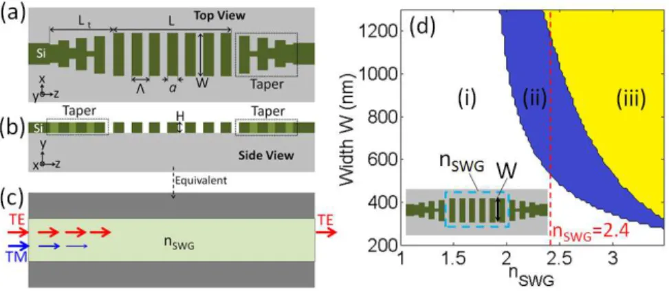
2. Polarizer Design
The proposed TE-pass polarizer is implemented as a SWG waveguide in 220 nm SOI, as it is
schematically shown in Figs. 1(a) and 1(b). The main structural parameters are: the waveguide width W
and height H, the grating pitch Λ, and the polarizer length L. The SWG waveguide comprises alternating
media with high (silicon) and low (ai
r) refractive indices, with a period Λ along the light propagation
direction. The silicon segment length is denoted as a
, i.e. the grating duty ratio is η = a/Λ. SWG-wire
tapered transitions with a length L
tare used to couple the light between the SWG waveguide and the
input and output silicon wire waveguides [21]. In order to achieve the polarizer performance, vertically
asymmetric waveguide geometry, i.e., the upper cladding has a different refractive index than the buried
oxide (BOX) cladding layer, is necessary for achieving the cut-off condition for the TM mode. For
simplicity, the upper cladding is air.
Fig. 1 Schematics of the TE-pass polarizer based on a subwavelength grating (SWG) waveguide. (a) Device top view; (b) cross-section (side view); (c) the SWG-polarizer represented as an equivalent wire waveguide with an engineered core refractive index nSWG; and (d) 3 regions of the cut-off conditions of the SWG waveguide as a function of the SWG waveguide width W and the
index nSWG, for Si layer thickness H=220 nm: (i) the cut-off region with no guided mode supported; (ii) region supporting only the
fundamental TE-like Bloch mode; (iii) region supporting both the fundamental TE- and TM-like Bloch modes.
We first evaluate the Bloch mode [17] cut-off condition of the SWG waveguide using the finite element
method (FEM), by considering the SWG waveguide as an equivalent wire waveguide with an engineered
core refractive index n
SWG[Fig. 1(c)]. The value of n
SWGcan be controlled by selecting a specific duty ratio
η= a /Λ [22]. We assume the following parametersμ a free-space wavelength of
0=1550 nm, the refractive
index of air n
air=1, the refractive indices of silicon and the SiO
2of n
Si=3.476 and n
SiO2=1.444, respectively.
The Bloch mode cut-off conditions determined by the index n
SWGand the waveguide width W can be
observed in Fig. 1(d), for the waveguide height H=220nm, which is commonly used in silicon photonics
foundries. When the engineered refractive index n
SWGincreases from 1 (air) to 3.476 (silicon), the mode
cut-off condition of the SWG waveguide changes from no supported propagating mode (region i), to
supporting only the TE-like Bloch mode (region ii), and supporting both the TE- and TM-like Bloch modes
(region iii). Figure 1(d) shows that the index engineering of n
SWGcan be used to control the Bloch mode
cut-off condition. By modifying n
SWG, a range of waveguide widths can be selected where the SWG
waveguide can only support the TE Bloch mode [region ii in Fig. 1(d)], while the TM mode is cut-off and
radiated primarily to the Si substrate through the BOX layer.
Next, the pitch and duty ratio of the SWG waveguide are set to
Λ=300 nm and η=0.5, respectively,
transitional taper is set to 5 m, for the optimal trade-off between the device size and the taper loss. We
calculated the SWG-wire waveguide transition loss as 0.1 dB. As it was previously demonstrated [17], the
theoretical loss limit for this type of tapers indeed is very low, ~0.04 dB. Using the effective medium
approximation in SOI waveguides [22], the engineered refractive index of the SWG waveguide n
SWGis 2.4
with a duty ratio of
η=0.5. In our design, the grating pitch Λ is on the order of a few hundreds of
nanometers, while the pitch deviations due to fabrication inaccuracies are no more than several
nanometers. Consequently, the fabrication inaccuracies are not expected to affect
the grating’s
subwavelength operation regime. Since the equivalent core refractive index of the SWG n
SWGis modified
by changing the grating duty ratio
η, the fabrication inaccuracies on the grating duty ratio η will change
the engineered core refractive index n
SWG. However, as shown in Fig. 1(d), the polarizer can tolerate a
relatively broad range of n
SWGin region (ii), specifically 2< n
SWG<2.5 if the waveguide width is W=1100
nm. This corresponds to a
duty ratio range of 0.3< η <0.6, yielding a device which is substantially tolerant
to the duty ratio deviations. According to Fig. 1(d), a TE-pass polarizer can be implemented using an
SWG waveguide with width ranging from 550 nm to 1200 nm, therefore allowing a large fabrication
tolerance to waveguide width variations.
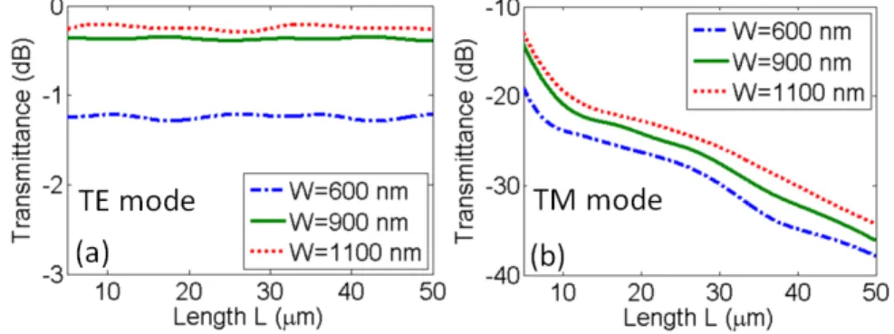
The performance of the proposed TE-pass polarizer is evaluated using the three-dimensional
finite-difference time-domain (3D-FDTD) simulations. The FDTD simulations include both the SWG-wire
taper sections and the periodic SWG polarizer section. Figure 2 shows the simulated transmittance for the
TE and TM modes for various SWG waveguide lengths (L) and widths (W)
, at the central wavelength of
0= 1550 nm. It is clear that the transmittance decreases with reducing the width W of the SWG waveguide.
It can also be observed that the SWG length L has a negligible effect on the TE mode, while the TM
mode attenuation substantially increases with L
.
In our nominal design, the width of the SWG waveguide
is set to W=1100 nm.
Fig. 2 Calculated transmittance of the TE-pass polarizer as a function the SWG waveguide length L for different widths W. H=220 nm, Λ = 300 nm, η=0.5, and 0 = 1550 nm. Calculated by the 3D–FDTD method with the grid
size Δx=20 nm, Δy=30 nm and Δz=20 nm and a time step t = 20 ps.
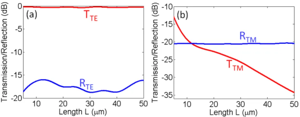
Figure 3 shows the calculated transmission (T
TEand T
TM) and reflection (R
TEand R
TM) coefficients for
the TE and TM input modes as a function of the SWG length L. Here, we define the transmission T and R
as T=P
out/P
inand R=P
back/P
in, respectively. P
in, P
outand P
backare the input, output and back-reflected
mode power, respectively. The TE mode exhibits a low waveguide propagation loss, including the
SWG-wire transition loss. On the other hand, the TM mode attenuates exponentially and leaks away from
the waveguide core, primarily to the silicon substrate. The reflection coefficients for both the TE and TM
polarizations are below
–
15 dB and are not significantly affected by the SWG waveguide length L. For the
waveguide width W=1100 nm, the SWG length L of 10 m yields a polarization extinction ratio (ER) of 20
dB. In our device, the SWG waveguide leng
th is chosen as L=50 m, for a polarization extinction ratio ER
Fig. 3 The polarizer transmission and reflection coefficients as a function of the SWG waveguide length L for (a) TE-like mode (TTE
and RTE) and (b) TM-like mode (TTM and RTM). W=1100 nm, H=220 nm, Λ = 300 nm, η=0.5, and 0 = 1550 nm. Calculated by the
3D–FDTD method with the grid size Δx=20 nm, Δy=30 nm and Δz=20 nm and a time step t = 20 ps.
Fig. 4 Light field evolution (|E|) along the TE-pass polarizer, as calculated by the 3D-FDTD method. Top view (x-z plane), input is located at the left port. (a) TE input and (b) TM input. W = 1100 nm, H = 220 nm, L = 50 µm, Lt= 5 µm, Λ = 300 nm, η = 0.5, and 0
= 1550 nm.
Figures 4(a) and 4(b) show the light field evolution in the TE-pass polarizer for the wavelength of
1550 nm. It is observed that the TE polarized light propagates in the structure with a low loss, while the
TM polarization is efficiently attenuated. Figure 5 shows the calculated transmission (T) and reflection (R)
coefficients as a function of wavelength (
). The transmission coefficient for the TE polarization, T
TE( ), is
about
–0.3 dB, while the TM polarization, T
TM( ) is very low (<–35 dB), in a broad wavelength range from
1450 nm to 1650 nm. The calculated reflection R for the TE and TM polarizations are <
–16 dB and <–20
dB, respectively, at
0= 1550 nm. The transmission loss and the reflections are mainly attributed to the
SWG-wire taper sections.
Fig. 5 Calculated wavelength dependence of polarizer transmission (T) and reflection (R) coefficients. Structural parameters: W = 1100 nm, H = 220 nm, L = 50 m, Lt = 5 µm, Λ = 300 nm, and η = 0.5. Calculated by the 3D–FDTD method with the grid size Δx=20
3. Fabrication and Experimental Results
The polarizer was fabricated on a silicon-on-insulator substrate with a 220 nm silicon waveguide layer and
a 2 m BOX layer. The e-beam lithography was used to pattern the polarizer structure and the
interconnecting waveguides under an etch mask of a high-contrast hydrogen silsesquioxane (HSQ) resist.
An inductively coupled plasma reactive ion etching (ICP-RIE) was used to transfer the waveguide layout
onto the silicon layer. The total device length including the SWG (L=50 m) and the taper sections
(2L
t=10 m) is 60 m. The images of the fabricated polarizer are shown in Fig. 6.
Fig. 6 (a) Optical microscope image of the fabricated polarizer; (b) SEM images of the transition taper section (left) and the periodic SWG polarizer section (right).
To experimentally characterize the polarizer performance, a tunable laser was coupled into the chip
using a polarization maintaining lensed fiber with a Gaussian beam waist of ~3 m and a polarization
controller, as shown in Fig. 7(a). To determine the reflection coefficients, an optical fiber circulator was
used at the input of the chip, as shown in Fig. 7(b).
Fig. 7 Experimental setups for (a) transmission and (b) reflection measurements. PC: Polarization Controller, PMF: Polarization Maintaining Fiber.
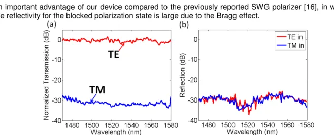
Figure 8(a) shows the measured transmission coefficients for the TE and TM polarized inputs. The
fiber-chip coupling loss and the measurement system loss were subtracted by using an independent loss
measurement on a set of straight reference waveguides. The average loss for the TE mode is ~ 0.4 dB
and the polarization extinction ratio is ~30 dB, within the wavelength range from 1470 nm to 1580 nm.
The measured polarization ER is close to the calculated value (35 dB). As it is shown in Fig. 8 (b), the TE
and TM reflection coefficients are about
–30 dB. Since the reflection response of the TM mode is similar
to that of the TE mode, we conclude that the reflection of the TM polarization is low, and the measured
reflected power is mainly due to reflections from the chip facet. This efficient suppression of reflectivity is
an important advantage of our device compared to the previously reported SWG polarizer [16], in which
the reflectivity for the blocked polarization state is large due to the Bragg effect.
Fig. 8 Experimental characterizations of the TE-pass SWG waveguide polarizer: (a) Measured TE and TM transmission coefficients (normalized to the transmittance of the reference Si-wire waveguide). (b) Measured TE and TM reflection coefficients.
4. Conclusion
We have proposed and experimentally demonstrated a low loss TE-pass polarizer based on a
subwavelength grating (SWG) waveguide. Our polarizer exploits for the first time the Bloch mode cut-off
condition by engineering the SWG equivalent material index. We show both by calculations and
experiments that only the TE mode is supported in the SWG waveguide while the TM mode attenuates
and leaks away to the silicon substrate with a low reflection. The experimental results for a devices
implemented in an SOI substrate with a 220 nm silicon layer yield an average TE insertion loss of 0.4 dB
in a broad wavelength range 1470 nm - 1580 nm, with a remarkably high polarization extinction ratio (~30
dB). The overall device length is 60 m. This work paves a promising way in development of compact
low-loss, low-reflectivity and fabrication tolerant silicon-based polarizing components operating over a
broad wavelength range.
References
[1] D. Dai, L. Liu, S. Gao, D.-X. Xu, and S. He, “Polarization management for silicon photonic integrated circuits,” Laser Photon. Rev., vol. 7, no. 3, pp. 303–328, May 2013.
[2] D. Dai, Z. Wang, and J. E. Bowers, “Ultrashort broadband polarization beam splitter based on an asymmetrical directional coupler,” Opt. Lett., vol. 36, no. 13, pp. 2590–2592, Jul. 2011.
[3] H. Qiu, Y. Su, P. Yu, T. Hu, J. Yang and X. Jiang, “Compact polarization splitter based on silicon grating-assisted couplers,” Opt. Lett., vol. 40, no. 9, pp. 1885–1887, Apr. 2015.
[4] H. Zhang, S. Das, Y. Huang, C. Li, S. Chen, H. Zhou, M. Yu, P. Guo-Qiang Lo, and J. T. L. Thong, “Efficient and broadband polarization rotator using horizontal slot waveguide for silicon photonics,” Appl. Phys. Lett., vol. 101, no. 2, p. 021105, Oct. 2012.
[5] Y. Xiong, D.-X. Xu, J. Schmid, P. Cheben, S. Janz, and W. Ye, “Robust silicon waveguide polarization rotator with an amorphous silicon overlayer,” IEEE Photonics J., vol. 6, no. 2, p. 2200308, Apr. 2014.
[6] L. Chen, C. R. Doerr, and Y.-K. Chen, “Compact polarization rotator on silicon for polarization-diversified circuits,” Opt. Lett., vol. 36, no. 4, pp. 469–471, Feb. 2011.
[7] A. V. Velasco, M. L. Calvo, P. Cheben, A. Ortega-Moñux, J. H. Schmid, C. A. Ramos, I. M. Fernandez, J. Lapointe, M. Vachon, S. Janz, and D.-X. Xu, “Ultracompact polarization converter with a dual subwavelength trench built in a silicon-on-insulator waveguide,” Opt. Lett., vol. 37, no. 3, pp. 365–367, Feb. 2012.
[8] L. Liu, Y. Ding, K. Yvind, and J. M. Hvam, “Silicon-on-insulator polarization splitting and rotating device for polarization diversity circuits,” Opt. Express, vol. 1λ, no. 13, pp.12646–12651, Jun. 2011.
[9] H. Guan, A. Novack, M. Streshinsky, R. Shi, Q. Fang, A. E.-J. Lim, G.-Q. Lo, T. Baehr-Jones, and M. Hochberg, “CMOS-compatible highly efficient polarization splitter and rotator based on a double-etched directional coupler,” Opt. Express, vol. 22, no. 3, pp. 2489-2496, Feb. 2014.
[10] Y. Xiong, D.-X. Xu, J. H. Schmid, P. Cheben, S. Janz, and W. N. Ye, “Fabrication tolerant and broadband polarization splitter and rotator based on a taper–etched directional coupler,” Opt. Express, vol. 22, no. 14, pp. 17458-17465, Jul. 2014.
[11] M. Z. Alam, J. Stewart Aitchison, and M. Mojahedi, “Compact and silicon-on-insulator-compatible hybrid plasmonic TE-pass polarizer,” Opt. Lett., vol. 37, no. 1, pp. 55-57, Jan. 2012.
[12] Y. Huang, S. Zhu, H. Zhang, T. Y. Liow, and G. Q. Lo, “CMOS compatible horizontal nanoplasmonic slot waveguides TE-pass polarizer on silicon-on-insulator platform,” Opt. Express, vol. 21, no. 10, pp. 12790–12796, May 2013.
[13] Y. Cui, Q. Wu, E. Schonbrun, M. Tinker, J.-B. Lee, and W. Park, “Silicon-based 2-D slab photonic crystal tm polarizer at telecommunication wavelength,” IEEE Photon. Technol. Lett., vol. 20, no. 8, pp. 641–643, Apr. 2008.
ridge optical waveguides,” Opt. Express, vol. 18, no. 26, pp. 27404–27415, Dec. 2010.
[15] Q. Wang, and S. T. Ho, “Ultracompact TM-pass silicon nanophotonic waveguide polarizer and design,” IEEE Photonics J., vol. 2, no. 1, pp. 49–56, Feb. 2010.
[16] X. Guan, P. Chen, S. Chen, P. Xu, Y. Shi, and D. Dai, “Low-loss ultracompact transverse-magnetic-pass polarizer with a silicon subwavelength grating waveguide,” Opt. Lett., vol. 3λ, no. 15, pp. 4514-4517, Aug. 2014.
[17] R. Halir, P. J. Bock, P. Cheben, A. Ortega-Moñux, C. Alonso-Ramos, J. H. Schmid, J. Lapointe, D.-X. Xu, J. G. Wangüemert-Pérez, Í. Molina-Fernández and S. Janz, “Waveguide sub-wavelength structures: a review of principles and applications,” Laser Photon. Rev., vol. λ, no. 1, pp. 25-49, Sep. 2014.
[18] P. J. Bock, P. Cheben, J. H. Schmid, J. Lapointe, S. Janz, G. C. Aers, D.-X. Xu, A. Densmore, and T. J. Hall, “Subwavelength grating periodic structures in silicon–on–insulatorμ a new type of microphotonic waveguide,” Opt. Express, vol. 18, no. 1λ, pp. 20251–20262, Sep. 2010.
[19] P. Cheben, D.-X. Xu, S. Janz, and A. Densmore, “Subwavelength waveguide grating for mode conversion and light coupling in integrated optics,” Opt. Express, vol. 14, no. 14, pp. 46λ5–4702, May 2006.
[20] Y. Xiong, J. G. Wangüemert-Pérez, D.-X. Xu, J. H. Schmid, P. Cheben, S. Janz, and W. N. Ye, “Polarization splitter and rotator with subwavelength grating for enhanced fabrication tolerance,” Opt. Lett., vol. 3λ, no. 24, pp. 6λ31-6934, Dec. 2014. [21] P. J. Bock, P. Cheben, J. H. Schmid, J. Lapointe, A. Delâge, D.-X. Xu, S. Janz, A. Densmore, and T. J. Hall, “Subwavelength
grating crossings for silicon wire waveguides,” Opt. Express, vol. 18, no.15, pp. 16146–16155, Jul. 2010.
[22] J. H. Schmid, P. Cheben, P. J. Bock, R. Halir, J. Lapointe, S. Janz, A. Delâge, A. Densmore, J.-M. Fédeli, T. J. Hall, B. Lamontagne, R. Ma, Í. Molina-Fernández, and D.-X. Xu, “Refractive index engineering with subwavelength gratings in silicon microphotonic waveguides,” IEEE Photonics J. vol. 3, no. 3, pp. 5λ7–607, Jun. 2011.