AlGaN/GaN-based Power Semiconductor Switches
by
Bin Lu
B.S., Tsinghua University (2006)
S.M., Massachusetts Institute of Technology (2007)
ARCHIMS
OF TECHNOLOGY
JLBRAR3
LIBRARIES
Submitted to the Department of Electrical Engineering and Computer Science in Partial Fulfillment of the Requirements for the Degree of
Doctor of Philosophy at the
MASSACHUSETTS INSTITUTE OF TECHNOLOGY
June 2013
@ 2013 Massachusetts Institute of Technology. All rights reserved
Signature of A uthor ... ... ... Department of Electrical Engineering and Computer Science
March 18, 2013
C ertified by ... Certifed byTomis ...Palaciosio ssociate Professor of Electrical Engineering Thesis Supervisor
A ccepted by... ... r. . . ... ...
7
Leslie A. KolodziejskiProfessor of Electrical Engineering Chair, Department Committee on Graduate Students
AlGaN/GaN-Based Power Semiconductor Switches
by
Bin Lu
Submitted to the Department of Electrical Engineering and Computer Science On March 18, 2013 in Partial Fulfillment of the
Requirements for the Degree of Doctor of Philosophy
ABSTRACT
AlGaN/GaN-based high-electron-mobility transistors (HEMTs) have great potential for their use as high efficiency and high speed power semiconductor switches, thanks to their high breakdown electric field, mobility and charge density. The ability to grow these devices on large-diameter Si wafers also reduces device cost and makes them easier for wide market adoption. However, the development of AlGaN/GaN-based power switches has encountered three major obstacles: the limited breakdown voltage of AlGaN/GaN transistors grown on Si substrates; the low performance of normally-off AlGaN/GaN transistors; and the degradation of device performance under high voltage pulsed conditions. This thesis studies these issues and presents new approaches to address these obstacles.
The first part of the thesis studies the breakdown mechanism in AlGaN/GaN-on-Si transistors. A new quantitative trap-limited space-charge impact-ionization model-is developed. Based on thmodel-is model, a set of design rules model-is proposed to improve the breakdown voltage of AlGaN/GaN-on-Si transistors. New technologies have also been demonstrated to increase the breakdown voltage of AlGaN/GaN-on-Si transistors beyond
1500 V.
The second part of the thesis presents three technologies to improve the performance of normally-off AlGaN/GaN transistors. First, a dual-gate normally-off MISFET achieved high threshold voltage, high current and high breakdown voltage simultaneously by using an integrated cascode structure. Second, a tri-gate AlGaN/GaN MISFET demonstrated the highest current on/off ratio in normally-off GaN transistors with the enhanced electrostatic control from a tri-gate structure. Finally, a new etch-stop barrier structure is designed to address low channel mobility, high interface density and non-uniformity issues associated with the conventional gate recess technology. Using this new structure, normally-off MISFETs demonstrated high uniformity, steep sub-threshold slope and a record channel effective mobility.
The thesis concludes with a new dynamic on-resistance measurement technique. With this method, the hard- and soft-switching characteristics of GaN transistors were measured for the first time.
Thesis Supervisor: Tomis Palacios
Acknowledgement
The past five and half years are a very important period in my life. The training I received at Palacios's group at MIT not only makes me a better researcher but also a comprehensive person. During these years, many people have helped me along the way and I would like to express my deepest gratitudes to them:
First, I would like to thank my advisor Prof. Tomis Palacios. I am very lucky to be his student and have the opportunity to work on a very exciting research topic. His insights, encouragement, patience and trust always motivate me to work on new ideas and approaches. The knowledge I learnt from him, not only in technical but also in many other aspects, will be invaluable in my life.
Second, I would like to thank my thesis committee Prof. Dimitri Antoniadis, Prof. Jesns del Alamo and Prof. David Perreault. Their insights, advices and encougragement greatly helped me to form a deeper understanding in device physics and power electronics circuits.
Thirdly, I would like to thank my colleagues in Palacios's group. Former group members Jinwook Chung and Xu Zhao provided a foundation for me to start with. Omair Saadat helped me with his knowledge on gate dielectric deposition. Dr. Elison Matioli helped with interference lithography and many overnight ebeam-lithography for the ARPA-E project. Dr. Mohamed Azize helped me with Raman measurement and gave many advices on strain relaxation in nitride semidoncutors. Min Sun helped greatly on the etch-stop structure device fabrication. Daniel Piedra was always my overnight cleanroom buddy. I enjoyed discussion with Feng Gao on device reliability. I also learnt about RF devices from Dongseup Lee and graphene electronics from Allen Hsu and Han Wang. The limited space does not allow me to enumerate everyone but all Palacios's group members are generous to share their knowledge with me. I should not forget the other 6 -floor fellows and friends I met at MIT. Their friendship enriches my life with fun. I shall thank all the staffs at Microsystems Technology Laboratories (MTL) who tiredlessly keep the. lab running smoothly.
Finally, I am very grateful to my mother Jianhua Zhang and father Zhenguo Lu for their endless love and support. My lovely wife Yan Jiang has always been supportive and understanding. I owe so much to you all. This thesis is dedicated to you.
Table of Content
Chapter 1 Introduction ...
23
1.1 Power Semiconductor Switches... 23
1.2 Design Constrains in Power Semiconductor Switches ... 24
1.3 The Status of Si Power Switches ... 27
1.4 Wide Bandgap Semiconductors... 28
1.5 Challenges in AlGaN/GaN-based Power Switches ... 31
1.6 T hesis O utline ... . 33
Chapter 2 Breakdown Mechanism of AlGaN/GaN-on-Si
Transistors ...
35
2 .1 Introdu ction ... 35
2.2 Low Breakdown Voltage in AlGaN/GaN-on-Si Transistors ... 36
2.3 Vertical Leakage Mechanism in AlGaN/GaN-on-Si Transistors ... 39
2.3.1 Vertical I-V and CV Characterization ... 39
2.3.2 Trap-Limited Space-Charge Model (TLSC Model) ... 43
2.3.3 Impact Ionization Model... 52
2.3.4 Trap-Limited Space-Charge Impact-Ionization Model (TLSCII Model)... 56
2.3.5 Vertical Breakdown of AlGaN/GaN-on-Si Structures: Negative Bias Condition. 58 2.3.6 Vertical Breakdown of AlGaN/GaN-on-Si Structures: Positive Bias Condition.. 61
2.3.7 Guideline for the Maximum Breakdown Voltage Design of GaN-on-Si Wafers.. 67
2.4 Schottky-drain Technology... 72
2.4.1 D evice Fabrication ... 73
2.4.2 D C Characterization... 74
2.5 Si Substrate Removal Technology... 76
2.5.2 Device Characterization... 77
2.6 Conclusion ... 80
Chapter 3 Normally-off GaN Transistors...83
3.1 Introduction... 83
3.2 Review of Normally-off GaN Transistor Technologies ... 84
3.2.1 Fluorine-treatment Technology ... 85
3.2.2 P-type Sem iconductor Gate Technology ... 85
3.2.3 Surface Potential Engineering Technology ... 86
3.2.4 Gate-recess Technology... 86
3.3 Dual-gate Norm ally-off GaN Transistors ... 87
3.3.1 Device Fabrication... 89
3.3.2 DC Characterization... 90
3.3.3 Characterization of Recessed-gate Channel... 92
3.4 Tri-gate Normally-off GaN Transistors ... 95
3.4.1 Device Fabrication... 95
3.4.2 DC Characterization... 97
3.4.3 Characterization of Tri-gate Channel Resistance ... 102
3.5 Impact of Sidewall-gates on Tri-gate AlGaN/GaN Transistors... 103
3.5.1 Device Fabrication... 103
3.5.2 DC Characterization... 104
3.5.3 CV Simulation ... 107
3.5.4 Tri-gate Channel M obility ... 119
3.5.5 Strain Relaxation in Tri-gate Structure ... 121
3.6 GaN Etch-Stop Barrier Structure ... 128
3.6.2 Surface Characterization ... 130
3.6.3 D C C haracterization... 132
3.6.4 C V Sim ulation ... 136
3.7 C onclusion ... 142
Chapter 4 Dynamic On-resistance Measurement ... 145
4 .1 Introdu ction ... 145
4.2 Dynamic Ron Measurement Technique ... 147
4.3 Dynamic Ron Extraction in Soft-switching and Hard-switching Circuits... 149
4.3.1 G ate D river C ircuit ... 150
4.3.2 Dynamic Ron in Soft-switching Condition ... 151
4.3.3 Dynamic Ron in Hard-switching Condition... 153
4.4 Effect of Soft-switching and Hard-switching on Dynamic Ron ... . . . .. . . .. 155
4 .5 C on clu sion ... 157
Chapter
5
Conclusions and Future W ork...159
5 .1 C on clu sion s... 159
5 .2 F uture w ork ... 160
5.2.1 Improving device breakdown voltage... 160
5.2.2 Higher threshold voltage normally-off device... 160
5.2.3 Understanding Trapping and Degradation Mechanism in AlGaN/GaN HEMTs 161
Appendix A Elasticity and Piezoelectricity in III-Nitride
Semiconductors ...
163
Appendix B Parameters of III-Nitride Semiconductors for CV
Simulations
...
167
Appendix C Nextnano3 CV Simulation Codes for Tri-Gate and
GaN-Etch-Stop Structure Devices ...
171
Appendix D Matlab Least-Square Fitting Codes for TLSC and
1LSC II M odels ...
199
List of Figures
Figure 1-1. On-off states of an idea power semiconductor switch. ... 24 Figure 1-2. Illustration of a non-punch-through depletion region in a reverse biased p*-n-n* diode, which the n-layer is fully depleted creating a positively charged space-charge region. Same depletion region can be found in other power semiconductor switches as well... 25 Figure 1-3. Illustration of electric field in super-junction reverse biased p-i-n diode. Same concept applies to the drift-region of a MOSFET. ... 28
Figure 1-4. Specific on-resistance RonxA as a function breakdown voltage Vbk for Si super-junction field-effect transistors (FETs), SiC MOSFETs and GaN AlGaN/GaN
high-electron-mobility-transistors (HEMTs) reported in literature... 30
Figure 2-1. Illustration of off-state leakage current in an AlGaN/GaN HEMT... 37 Figure 2-2. Buffer breakdown voltage as a function of contact distance measured in an AlGaN/GaN heterostructure grown on Si substrate with total epi-layer thickness of 2 pm. The inset schematic shows the testing device structure with Si substrate at floating potential. The breakdown voltage is defined as the voltage drop between the contacts at 1 mA/mm leakage cu rrent... 38
Figure 2-3. Cross-section scanning-electron-microscope (SEM) image of the wafer used in the study and schematics of two samples prepared for the electrical characterization... 39 Figure 2-4. Vertical conductance measurement of the Si( 111) substrate obtained by removing the G aN ep i-layer... 4 1 Figure 2-5. 1 kHz CV measurement of the MIS-cap structure on Si(1 11) substrate... 41 Figure 2-6. Vertical GaN-Si leakage measurement with (a) ohmic-contact sample 1 and (b) Al-Schottky-contact sample 2 at substrate temperature of 10 C, 50'C and 100*C. The top-contact size is 100 [tm x50 pm . ... 42 Figure 2-7. Vertical CV measurements with (a) ohmic top contact and (b) Schottky top contact on GaN-on-Si sample at 15 kHz. The top contact has a circular shape with a diameter of 180 gm. Inset in (a) shows the corresponding vertical I-V characteristics. The schematic show s the m easurem ent setup... 43 Figure 2-8. Schematics of the injected electrons uniformly distributed in the epi-layer at negative bias on the contact in the velocity saturation regime. The injected electrons create a linearly increasing electric field... 45
Figure 2-9. Band diagram illustrates the position of quasi-Fermi-level with respect to shallow and deep trap s. ... 46 Figure 2-10. Schematic of electric field in the TLSC model with different trap density in two
regions w ith N < N 2... 48 Figure 2-11. Calculated TLSC current in 2 pm GaN layer at 10 C and 100 C with three trap levels: Ec-0.55 eV, Ec-0.4 eV and Ec-0.3 eV. All have a density of 2x 1016cm-3 except the
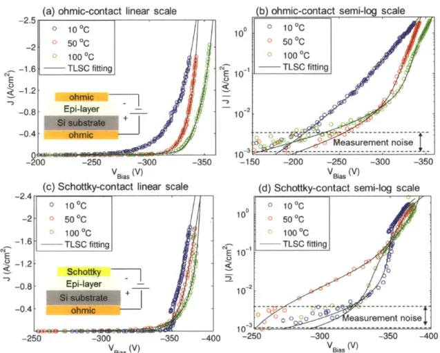
Ec-0.3 eV trap having a density of 3 x 10 16cm-3. The results are plotted in linear scale (a) and in log-log scale (b). ... 49 Figure 2-12. Fitting to the vertical leakage current measured on both ohmic-contact and
Schottky-contact samples at negative bias: (a) ohmic-contact sample plotted in linear scale (b) and semilog scale; (c) Schottky-contact sample plotted in linear scale (d) and semilog scale.
... 5 1
Figure 2-13. Illustration of impaction ionization initiated by electron current in an impact
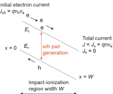
ionization region of w idth W ... 54
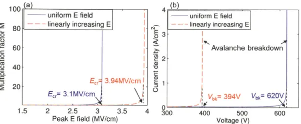
Figure 2-14. (a) Calculated impact ionization multiplication factor M as a function of peak electric field; and (b) corresponding current density as a function of voltage across a 2 pm G aN ep i-layer... 55
Figure 2-15. Illustration of the trap-limited space-charge impact-ionization (TLSCII) model with negative bias on the contact with respect to the Si substrate. The impact ionization is
initiated by electron injection... 57
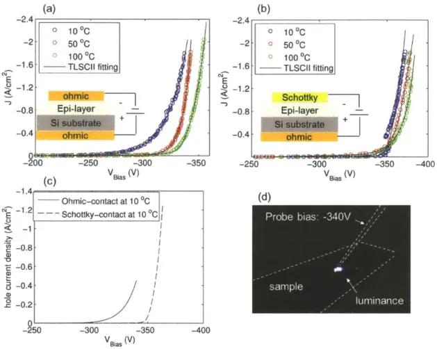
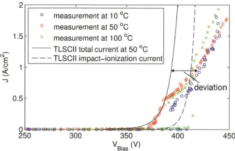
Figure 2-16. TLSCII model fitting to the measured vertical leakage current at negative bias conditions on (a) ohmic-contact sample and (b) Schottky-contact sample. (c) Extracted hole current density from the TLSCII model at 10 "C (d) Digital camera picture of luminance from the ohmic-contact sample at bias voltage around -340 V. ... 60
Figure 2-17. TLSCII model calculation result fitting to the measurement data of Al-Schottky contact sample under positive bias condition. ... 62
Figure 2-18. Illustration of the electron injection from p-Si substrate at positive bias condition where the electron injection is limited by the generation rate G in the depletion region of the p-type Si substrate. ... 63
Figure 2-19. CMOS camera image showing the luminance from the edge of an Al-Schottky-contact device biased at about 400 V with respect to the Si substrate measured at room tem p erature. ... 65
Figure 2-20. (a) Band diagram of forward biased ohmic contact illustrating the SRH generation at defect states created by the ohmic contact; (b) CMOS camera image of luminance from ohmic-contact metal at 200 V bias; (c) Cross-section
scan-electron-microscope (SEM) image of the ohmic contact on GaN used in the study... 66 Figure 2-21. Schematic of a buffer-breakdown test structure on a GaN-on-Si wafer with the
source-drain distance Lsd much larger than the epi-layer thickness d... 67
Figure 2-22. (a) Calculated avalanche breakdown voltage as a function of total epi-layer thickness on Si substrate with comparison to literature reported data; (b) Average trap density as a function of avalanche breakdown voltage for zero electron injection field from Si
substrate (Eo = 0). Increasing Eo results in a decreased trap density. ... 72
Figure 2-23. Si substrate potential measurement: (a) schematic of the measurement setup; (b) measured substrate potential as a function of VdS with three leakage current components; (c) voltage distribution among the source, drain and Si substrate... 73
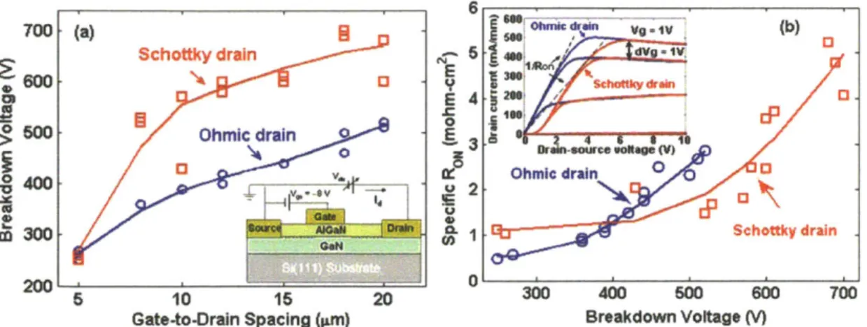
Figure 2-24. : I-V characteristics of Schottky-drian contact with and without recess etching on A lG aN ... 74 Figure 2-25. (a) Buffer lateral leakage current of the ohmic-drain and Schottky-drain devices with 14 [tm contact spacing; The inset shows the leakage current in semi-log scale and the measurement configuration; (b) buffer lateral breakdown voltage as a function of
source-to-drain spacin g ... 75
Figure 2-26. (a) Three-terminal breakdown voltages as a function of gate-to-drain distances;
(b) Specific Ro. as a function of breakdown voltages. The inset picture is the I-V curves of
the ohmic-drain and Schottky-drain devices with Lg = 2 gm, Lgs = 1.5 pm and Lgd = 10 im.76 Figure 2-27. Process flow of the substrate transfer technology. (a) Standard AlGaN/GaN HEMTs are fabricated; (b) Device surface is bonded to a Si carrier wafer and Si (111)
substrate is removal by SF6 plasma etching; (c) the N-face surface of the exposed
GaN/AlGaN buffer is then bonded to a glass wafer; (d) After releasing the Si carrier wafer, the device is successfully transferred to the glass wafer... 77
Figure 2-28. (a) I- Vd characteristics of AlGaN/GaN-on-glass after the substrate transfer and of AlGaN/GaN-on-Si before substrate transfer measured in DC bias condition; (b) Id-Vd
characteristics of an AlGaN/GaN-on-glass device measured at DC and 500-ps/200-ms drain pulse conditions at 25 C and 10 *C. All devices have same dimensions with Lg = 2 pm, Lgs =
L g = 1.5 p m ... 78 Figure 2-29. Two-terminal buffer breakdown voltage as a function of Lsd of devices before and after being transferred to a glass wafer. The data of the device transferred to the glass substrate can be fitted with a power law to the order of 1.5... 79
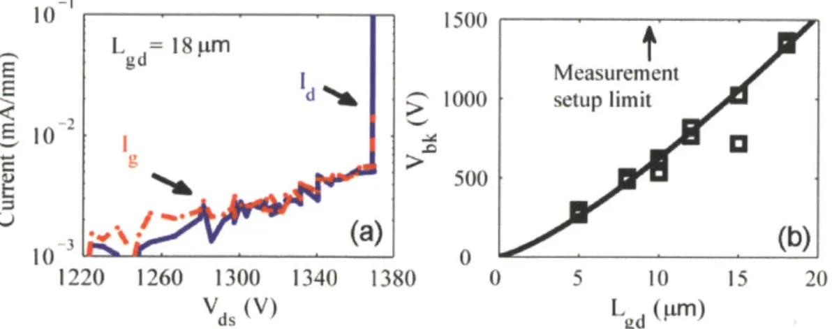
Figure 2-30. a) Three-terminal leakage current for an AlGaN/GaN HEMT on glass with Lgd=
18 pm at Vgs = - 8 V. For Vds < 1220 V, the leakage current is below the sensitivity of the measurement setup (1 gA/mm). (b) Three-terminal Vbk as a function of Lgd. ... 80 Figure 3-1. Circuit schematic of a D-mode GaN transistor in a cascode configuration with a norm ally-off transistor. ... 83
Figure 3-2. Normally-off AlGaN/GaN transistors fabricated by: (a) fluorine-treatment technology, (b) p-type gate technology, (c) surface potential engineering technology, and (d) gate-recess technology ... 84 Figure 3-3. Dual-gate normally-off AlGaN/GaN transistor designs in two different gate configuration s ... 88
Figure 3-5. Schematic of integrated dual-gate normally-off transistor and simulation of potential profile at drain voltage of 100 V... 89
Figure 3-6. Cross-section SEM image of the gate recess in the dual-gate normally-off
tran sistor... 90
Figure 3-7. (a) I- Vds characteristics of an integrated dual-gate E-mode device with Lgd 5 pm; (b) Transfer characteristics of the E-mode device compared to a D-mode device of the same structure without gate recess. The E-mode device is biased at Vds = 12 V and the
D-m ode device is biased at Vds = 10V ... 91
Figure 3-8. Three-terminal breakdown measurement of an E-mode device at Vgs = 0 V and a
D-mode device at Vgs = -8 V and -6.8 V. Both devices have Lgd = 8 ptm. The current
Figure 3-9. Ron as a function of recessed-gate lengths. The extrapolation to zero recessed-gate length gives a resistance of 6.74 ohm-mm,-which is the Ro. (6.76 Q-mm at Vgs = 7 V) of a
standard D-mode device with the same dimensions... 93
Figure 3-10. Field-effect mobility UFE and saturation mobility Usat of the E-mode dual-gate transistor calculated from gm- Vd characteristics at Vd= 0.1 V and 12 V... 94 Figure 3-11. Tri-gate device fabrication: (a) PECVD Si0 2 mask deposition and 660 nm tri-gate region pre-definition etching; (b) Interference lithography and subsequent dry etching; (c) 120-nm AlGaN gate-recess region lithography and recess-etching. Atomic-force-microscope (AFM) image shows the profile; (d) gate dielectric deposition and gate metallization. The cross-section scanning-electron-microscope (SEM) images show the dimensions of the tri-gate channel structure which has a period of 300 nm. The top channel width is 90 nm and the sidewall height is 250 nm. (e) Schematic of the Lloyd's mirror interference system used in the fabrication (source: Nano Structures Laboratory Lloyd's mirror interference lithography user manual) ... 97
Figure 3-12. Comparison of a tri-gate normally-off GaN MISFET with a standard planar-gate D-mode GaN transistor: (a) transfer characteristics at Vs = 1, 3, and 5 V with bi-direction
gate sweep; (b) Id- Vds characteristics. Both devices have Lgs = 1.5 pLm, Lg = 2 pm, Lgd = 10 pm and W = 100 pm ... ... 98
Figure 3-13. Ids- Vgs characteristics of the tri-gate normally-off MISFET compared with the standard planar-gate transistor and the recessed-gate MISFET with recessed-gate length of
160 nm. All the devices have the same dimensions with Lgd = 8 pm and are biased at Vs - 1 V (solid) and 3 V (dashed)... 99
Figure 3-14. Three-terminal BV measurement of the tri-gate normally-off GaN MISFET with Lgd = 10 pm at Vgs = 0 V . ... 101 Figure 3-15. (a) Specific on-resistance (Ron,sp) vs. breakdown voltage (BV) and (b) leakage current vs. BV of the tri-gate normally-off GaN MISFETs and other normally-off GaN devices in the literature with BV measured at Vgs = 0 V. ... 101
Figure 3-16. Ro. as a function of source-to-drain distance Lsd extracted at Vgs = 7 V. The R.n
of normally-off tri-gate devices is on average 1.2-1.8 Q-mm higher than that of standard planar-gate devices... 102 Figure 3-17. Cross-section schematic of the tri-gate channel of the fabricated devices... 104
Figure 3-18. Transfer characteristics of a planar-gate transistor (gate length of 10 pm) and tri-gate transistors (tri-tri-gate length of 15 pm) with side-wall height of 70 nm, 120 nm, 200 nm and 350 nm at Vs = 1 V. The current is normalized by the channel width which is 150 nm for
every 370 nm width for tri-gate transistors and 100 pim for planar-gate transistor. Vgs is stepped from negative to positive direction... 105
Figure 3-19. Quasi-static CV measurement of tri-gate capacitors with side-wall height of 70 nm, 120 nm, 200 nm and 350 nm and planar-gate capacitors. Bias votlage was swept from negative to positive direction. The cross-section schematic of one unit tri-gate structure
shows the capacitor components of Ctop, Cside-wait and Cbottom. The capacitance is normalized
by the top channel area. ... 107
Figure 3-20. (a) Net polarization charges and polarization dipole moments in the SiO2/GaN/Al0.26Ga0.74N/GaN structure with AlGaN lattice matched to GaN; (b) Band
diagram of the planar-gate device without SiO2/GaN-cap interface charges and (c) with
appropriate positive charge added to the SiO2/GaN-cap interface. ... 110
Figure 3-21. Simulated CV characteristics of planar-gate device fitted well with the
m easurem ent result. ... 111 Figure 3-22. Measured and simulated CV curves of 70-nm-sidewall tri-gate device. The different CV simulations compare the impacts of the tri-gate sidewalls, strain relaxation and SiO2/GaN-cap interface charges on the shift of pinch-off voltage. Open circle is the tri-gate
simulation with full strain and the same interface positive fixed charge as in the planar-gate device; Cross and diamond are the results by reducing the piezoelectric charges due to strain relaxation; Filled-circles represent the simulation fitted to the measurement by changing the SiO2/GaN-cap interface positive charges. Planar-gate CV curve is for comparison purpose.
... 1 13
Figure 3-23. Simulated 2D plots of the conduction band edge of the 70-nm-side-wall tri-gate device at gate bias of 0 (a) and -3 V (b) with 1D slices at X = 0 and Y = 50 nm positions. The
plot in (c) compares the conduction band energy at y = 50 nm and 20 nm positions in (b). 115
Figure 3-24. Electron density of the 70-nm-side-wall tri-gate device at gate bias of 0.5 V, 0 V an d -3 V ... 1 17
Figure 3-25. Simulated and measured CV curves of tri-gate devices with side-wall heights of
Figure 3-26. Simulated sidewall-gates (one pair) to 2DEG capacitance of each tri-gate structure unit shown in the inset schematic at Vg = 0 V. The capacitance is normalized to the tri-gate length direction perpendicular to the cross-section schematic inset. The simulation assumes an ideal side-wall interface without trap states... 119
Figure 3-27. (a) R0 as a function of tri-gate length Lig; (b) simulated 2DEG density with
planar-device as a reference; (c) calculated effective 2DEG mobility; of the 70-nm-side-wall tri-gate tran sistors... 12 1
Figure 3-28. Raman spectrum of the planar AlGaN/GaN-on-Si(1 11) sample (a) with laser
focal point in the GaN channel layer; (b) with the laser focal point in the buffer layer. The dots are the measurement data; the red-solid lines are Lorentzian fitting; the green-colored line is the total fitting curve by two Lorentzians. ... 123
Figure 3-29. GaN E2 (high) Raman shifts as a function of tri-gate side-wall heights. Each data point is averaged from 15-20 measurements... 124 Figure 3-30. Schematic of boundary conditions used in the finite-element piezoelectricity sim u lation ... 126 Figure 3-31. Simulated x-axis strain component exx of the tri-gate structure with different
side-w all h eights. ... 126
Figure 3-32. (a) Simulated piezoelectric charge density as a function of tri-gate height at
interfaces of GaN-cap/AlGaN and AlGaN/GaN and at the surface of GaN-cap layer; (b) inverse of sheet resistance of tri-gate channel as a function of tri-gate height before deposition of gate dielectric. The dashed line is to guide the eyes. Sheet resistance Rsh was measured with halogen lamp light illumination on the devices to reduce the side-wall
depletion. Tri-gate height of 0 represents the planar device... 127 Figure 3-33. (a) Band structure and electron density profile of the new wafer structure. (b) Recess depth as a function of etch duration. The depth was measured by atomic force
microscope (AFM). Inset shows the relevant dimensions of a recessed-gate GaN MISFET.
... 12 9
Figure 3-34. XPS measurement of the sample surface (a) after the 350s BCl3/SF6 dry etching;
(b) showing the reduction in F Is signal after 02 plasma treatment and 1 min TMAH wet etch.
Figure 3-35. XPS atomic ratio of Al2p / (Al2p + Ga3d) as a function of TMAH wet-etch time at 70 *C (red circles) and as a function of oxidation / TMAH etch cycles (diamonds). The zero point in x-axis is after 350 s BCl3/SF6 dry etching removing the n-GaN layer. A data
point (square) also shows the result after 1 cyc of 02/TMAH followed by 1 cyc of
UV-ozon e/H C l. ... 132
Figure 3-36. (a) Id- Vgs characteristics at VdS = 0.1 V with bi-directional gate sweep; (b) I- Vds
characteristics. The recessed-gate transistor has Lrec-g = 3 [tm and Lgs = Lgd = 4 pm. The
planar-gate transistor (dashed line) has the same Lsd with Lg 8 pm and Lgs = Lgd = 1.5 pm. ... 13 3
Figure 3-37. C-V characteristics of the recessed-gate capacitor measured at 1 kHz (solid line)
and 1 MHz (dashed line) with bi-directional sweeps. Inset zooms in the dashed rectangular
region . ... 133 Figure 3-38. (a) Ron as function Lree.g at Vgs = I to 3 V. The slope of each curve gives Rch. (b) pUe as a function of Nsh of the recessed-gate GaN MISFET extracted from DC/CV
m easurements and gated-Hall measurem ent... 135 Figure 3-39. Three-terminal BV measurement of the recessed-gate normally-off GaN
MISFET with Lrec-g = 3 jim, Lgd = 13 gm at Vgs = 0 V... 136
Figure 3-40. Simulated low-frequency (LF) and high-frequency (HF) CV characteristics
match with measured 1kHz and 1MHz CV curves. Inset zooms in the dashed rectangle region, showing the dispersion caused by interface states... 138 Figure 3-41. A1203/AlN interface trap density (Dit) vs. energy level relative to conduction
band edge of AlN (Ec-Etrap). The inset shows the location of the traps in the band structure of the device at zero bias voltage. ... 139 Figure 3-42. Simulated band diagram and electron density at Vgs = 0, 1, 2 and 3 V... 140 Figure 3-43. Simulated sheet electron density inside GaN and Alo.15Gao.85N with measured sheet electron density from 1 MHz CV and gated-Hall measurements... 141 Figure 3-44. Band diagram at flat-band condition showing the electric field (E-field)
direction in A 120 3... . . . . .. . . .. . . .. . . .. . . 142 Figure 4-1. Illustration of current collapse and increase of dynamic on-resistance Ron when an AlGaN/GaN HEMT is switched-on from high voltage off-state to on-state... 145
Figure 4-2. Illustration of charge trapped on the surface and in buffer of an AlGaN/GaN
H E M T . ... 14 6
Figure 4-3. Illustration of the current-voltage trace during the turn-on transition of a power transistor in hard-switching and soft-switching circuits. The turn-off transition is time reverse of th e trace... 14 6 Figure 4-4. (a) Voltage clamping circuit for Vdson measurement; (b) measured voltages from
the voltage clam ping circuit... 149
Figure 4-5. Gate drive circuit diagram... 150
Figure 4-6. Gate drive output waveform at 5 V... 151
Figure 4-7. Soft switching circuit diagram. ... 152
Figure 4-8. Soft-switching waveforms of GaN transistor (a) Vg and Vs (b) Vdson and 11+12 w aveform s... 152
Figure 4-9. Normalized dynamic Ro. of the GaN transistor and Si MOSFET in soft-switching condition at 2 ps after the peak Vds stress... 153
Figure 4-10. Hard-switching circuit diagram... 154
Figure 4-11. GaN transistor hard switching Vds, Id waveforms in (a) turn-on transient and (b) turn-off transient at 150 V Vds stress. The Vds rises to 150 V in (b) with a RC time constant of 40 ps of the input filter... 154
Figure 4-12. Normalized dynamic Ro. of the hard-switched GaN transistor and Si MOSFET at 2 ps and 10 ps after the devices were switched on. ... 155
Figure 4-13. (a) ARon of GaN transistors measured at 2 ps after the off-state peak Vs in hard-and soft- conditions; (b) turn-on transient Vds-Id traces from off-state voltage of 180 V... 156
Figure 4-14. (a) circuit diagram of the connection of 10 nF capacitor; (b) increase of dynamic Ron measured at 2 ps after the peak Vds; (c) Id- Vds traces of the hard-switching GaN transistor with 10 nF external capacitor during turn-on transient... 157
List of Tables
Table 1-1. Comparison of wide-band-gap semiconductors with Si [Sze&Ng]. ... 29 Table 2-1. Extracted Vo and effective Nt at different trap levels by least-square fitting to the vertical leakage measurement data of the negative biased ohmic-contact and Schottky-contact sam ples using the TLSC m odel. ... 52
Table 2-2. Extracted effective Nt at different trap levels by least-square fitting to the vertical leakage measurement data of the negative biased ohmic-contact and Schottky-contact samples using the TLSCII model. Dash means the corresponding Et is not used in the fitting.
... 5 9
Table 3-1. Channel resistance Rch (Q/sq), charge density Qch (X 1012 Cm-2) and electron mobility Pe (cm2
V-1s-1) as a function of Vgs (V) extracted from DC/CV measurements and gated-Hall measurement. Rch is too large at Vgs = 1 V to give a reliable Hall measurement. 134
Table 4-1. Comparison of datasheet value of IRF620 and EPC 1012... 150
Table A- 1 Elastic constants (GPa) [W right 1997]... 164
Chapter 1 Introduction
1.1 Power Semiconductor Switches
Power semiconductor switches are a type of semiconductor devices which control the flow of current in power electronics circuits for the conversion of electric power. Some of the applications where these switches are useful include High-Voltage-Direct-Current (HVDC) transmission systems, motor control systems, renewable energy generation systems, battery management systems, and consumer electronics, where electric power is converted between different voltages, current forms or frequencies.
Power semiconductor switches operate primarily in two states as shown in Figure 1-1. In the on-state, an ideal switch conducts current without any voltage drop. In the off-state, it holds off the voltage without any current conduction.
There are three types of power switches: diodes, thyristors and transistors. Diodes are two terminal p-n junction devices widely used in many power electronics circuits such as in the rectifier circuits for the conversion of alternating current (AC) into direct current (DC). Thyristors are three-terminal devices with multiple stacked p-n junctions. With very high voltage blocking and high current conduction capabilities, they find applications in most of the high power systems (mega-watts) such as the HVDC transmission systems. Finally, transistors are one of the most common three-terminal devices. Based on the type of carriers involved in current conduction, transistors are divided into two types. The first type is the unipolar transistor, in which only one type of carriers (electrons or holes) conducts the current. Examples are field-effect transistors (FETs), such as the metal-oxide-field-effect transistors (MOSFETs) and junction-field-effect transistors (JFETs). The second type is the bipolar transistor, in which both types of carriers are involved in current conduction. An example is the bipolar-junction transistor (BJT).1 There is also a special type of bipolar transistor, which combines an FET with a BJT, the insulated-gate-bipolar-transistor (IGBT).
1 Similar categorization also applies to diodes. For example, Schottky-diodes are unipolar devices while the p-n diodes are bipolar devices.
Section 1.2
In low voltage (less than 1 kV) to medium voltage (1 kV to about 50 kV) applications, power
MOSFETs and IGBTs are the predominant power switching devices due to their good turn-on/off capabilities and the high impedance of their insulating gate.
Current
On-state
0
Off-state
Voltage
Figure 1-1. On-off states of an idea power semiconductor switch.
1.2 Design Constrains in Power Semiconductor Switches
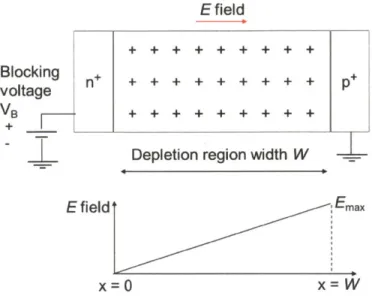
All the power semiconductor switches mentioned above have a lightly doped region for
blocking the off-state voltage. For example, in a p*-n-n* diode shown in Figure 1-2, depletion occurs in the lightly doped n-layer in the off-state reverse-bias condition..For an abrupt junction, the electric field in the depletion region increases linearly. The reverse bias
blocking voltage VB and the maximum electric field Emax satisfy:
2 _ EmaxW - qNdWD B 2 2es Emax = Es (1-1) (1-2)
where Nd is the doping density in the n-region, WD is the depletion width (less than the
n-layer thickness) and e, is the dielectric constant of the semiconductor material. 4
Chapter 1 Blocking voltage VB
+>1
E field n + ++ + + + + + + p*Depletion region width W
Emax
x = 0
Figure 1-2. Illustration of a non-punch-through depletion region in a reverse biased p*-n-n* diode, which the n-layer is fully depleted creating a positively charged space-charge region.
Same depletion region can be found in other power semiconductor switches as well.
When the Emax reaches the critical electric field Eer (also called breakdown electric field) of the semiconductor material, significant carrier generation occurs in the depletion region due to impact ionization and the semiconductor switch undergoes avalanche breakdown (see Chapter 2). The blocking voltage VB defined at the avalance breakdown condition is the breakdown voltage of the device.
When the depletion region extends into the n*-layer (the punch-through condition), breakdown voltage of the device will be smaller than the non-punch-through condition as shown in Figure 1-2, where the depletion region is confined in the lightly doped n-layer2. Here we consider the optimal condition when the n-layer thickness W is equal to the maximum depletion width at avalanche breakdown. Replacing Emax with Er in equation (1-1) and (1-2), we have
2 The detailed analysis of the punch-through condition can be found in reference [Sze&Ng].
Section 1.2
Vbk = EcrW (1-3)
Ecr = qNdW (1-4)
Es
Where Vbk is the breakdown voltage 3, Nd is the doping concentration in the lightly doped n-region and W is the n-n-region thickness.
Rearranging equation (1-3) and (1-4) gives
W 2Vbk (1-5)
Ecr
Nd= 2Er (1-6)
qVbk
For a certain voltage application, W and Nd can be determined from the above equations. The resistance per unit area of the lightly doped n-layer can be calculated by
R 4Vk 3 (1-7)
qyNd EsIEcr
where t is the carrier (electron in this example) mobility.
In unipolar power switches such as power MOSFETs and Schottky diodes, the resistance in this region contributes a significant portion of the total resistance, which limits their applications to mainly low voltage systems.
In bipolar power switches such as p*-n-n* diodes, thyristors and IGBTs, the resistance in the voltage blocking region is reduced by minority carrier injection so that they can carry a large current [Sze&Ng]. As a result, these devices are suitable for high voltage and high current applications. However, due to the injected minority carriers, these devices cannot return back to the high-impedance off-state immediately until the minority carriers disappear
3 This is the upper limit of breakdown voltage in a power semiconductor switch. Depending on device geometry, premature breakdown due to electric field crowding (edge effect [Sze&Ng]) before the maximum breakdown voltage is reached.
Chapter 1
in the voltage blocking region. This delay time is called reverse recovery time which limits the switching speed of these devices.
As a result, for a given semiconductor material, low voltage switches have faster switching speed than high voltage switches. It should be mentioned that this trend is also observed within the same category of power switches. For example, in power MOSFETs, the resistance in the voltage blocking region increases with the square of its breakdown voltage according to equation (1-7). In order to compensate the increase of resistance, larger device area is used, which results in a larger device capacitance. The larger capacitance in turn reduces the switching speed4. As we will see later, a good figure-of-merit to characterize the device performance is the product of its on-resistance Ron with its area A: RonxA. It is called specific on-resistance.
1.3 The Status of Si Power Switches
The semiconductor industry is dominantly built upon the single crystalline Si, which solely consists of the second most abundant element in the Earth's crust, Si (in the natural
form of SiO2). With the Si fabrication technology being the most advanced semiconductor technology, most of the electronic devices produced today are fabricated on Si wafers, so are the power semiconductor switches.
As shown in section 1.1, the switching speed of power semiconductor switches decreases as their breakdown voltage increases. This trend has a great significance in power electronics circuits. For example, the size of the energy storage components (e.g. inductors and capacitors) in a power electronics circuit scales inversely proportional with its operating frequency. The slow switching speed of power semiconductor switches results in bulky power electronics circuits especially in high voltage applications. Furthermore, higher switching frequencies also improve the transient response and stability of DC-DC power converters [Lehman 1996]. These limitations of Si power switches, determined by its intrinsic properties such as Eer and p, constitute an important bottleneck for power electronics circuits.
4 With larger device capacitance, the switching loss of the device is increased if the switching frequency is
Section 1.4
One way to improve the performance of Si power switches is to extend the use of the unipolar devices-power MOSFETs-to higher power applications, as their unipolar behavior allows for higher switching speeds. For this purpose, a super-junction (SJ) technology has been proposed [Deboyl998]. The basic concept of the super-junction technology is to change the electric profile in the device voltage blocking region by introducing narrow stripes of p-type regions to precisely match the stripes of n-type doping density. As shown in Figure 1-3, when the voltage blocking region is depleted, the space-charges in these stripes cancel each other and the electric field becomes uniform. The limitation on the doping density in equation (1-6) no longer applies. As a result, much higher doping density can be used to reduce the resistance of the voltage blocking region. However, the fabrication of these long stripes with very precise doping concentration is very challenging, especially for high voltage devices. As a result, the currently reported Si SJ-MOSFETs are expensive and their applications are limited to voltages below 1000 V [Deboy1998, Onishi2002, Rub2004, Sakakibara2008]. An alternative approach is to use new materials with intrinsically better characteristics than Si.
n
-_ p_ -_-p
+
+ + + nFigure 1-3. Illustration of electric field in super-junction reverse biased p-i-n diode. Same concept applies to the drift-region of a MOSFET.
1.4 Wide Bandgap Semiconductors
Wide bandgap semiconductors with higher critical electric field than Si can fundamentally improve the performance of power semiconductor switches. As shown in
Chapter 1
Table 1-1, SiC and GaN have about lOx higher critical electric field than Si. They are great candidates for higher performance power switches.5
Table 1-1. Comparison of wide-band-gap semiconductors with Si [Sze&Ng].
Property Si 4H-SiC Wurtzite GaN
Bandgap (eV) 1.12 3.2 3.4
Dielectric constant 11.9 10 10.4
Critical electric field (MV/cm)* ~0.3 ~4 ~4
Electron mobility (cm2
V's 1) 1350a 8 0 0b 850 , ~1100o
Thermal conductivity (Wcm"oCI) 1.5 4.9 1.7
f Actual value depends on electric field profile.
a. Room temperature low field mobility of bulk n-type Si with doping concentration of about 104
cm-3
. It varies between about 200 and 1350 cm2V's' for doping concentration between 1014 and 1018 cm-3[Sze&Ng].
b. Room temperature low field mobility of bulk n-type 4H-SiC at doping concentration of 1016 cm~3
. It varies between 200 and 950 cm2
V's1 for doping concentration between 10" and 1018 cm~3
[Roschke2001].
c. Room temperature low field mobility of bulk wurtzite n-type GaN at impurity concentration of 1017 cm-3
. It varies between 500 and 1150 cm2
V's' for impurity concentration between 1016 and 1018 cm-3 [Albrechtl998].
d. Room temperature peak effective mobility of two-dimensional-electron-gas (2DEG) in AlGaN/GaN heterostructure [Dangl999, Lu2013]. It varies between 800 and 1100 cm2
Vs s for
2DEG density between 3x 10¹² and 1013 cm-2
. It also varies with Al percentage in AlGaN due to alloy scattering.
The advantage of these wide bandgap semiconductors in power electronics can be
highlighted by plotting the specific on-resistance, Ro0 xA as a function of breakdown voltage
of the power switches, where Ro. is the device on-state resistance and A is its area (Figure 1-4). As discussed in Section 1.1, for high voltage unipolar devices such MOSFETs and
JFETs, Ro. is dominated by its voltage blocking region (the drift-region) resistance.
Therefore, we can use equation (1-7) to calculate the specific on-resistance:6
4Vik
Ron x A =
Es pEcr
s GaN-based devices also benefit from the high electron mobility in AlGaN/GaN heterostructure.
6 This equation assumes ideal electric field distribution in the depletion region as shown in Figure 1-2. It does not apply to lateral device geometry where electric field concentrates at junction edges (edge effect [Sze&Ng]). However, RouxA can still be used to bench mark device performance.
Section 1.4
As shown in Figure 1-4, the wide-band-gap semiconductor devices have three orders of magnitude lower specific on-resistance than the Si unipolar devices. As a result, low loss and high speed power devices can be made from these materials.
Another advantage of wide-band-gap semiconductors is their ability to operation at high temperatures due to very small intrinsic carrier concentration. For example, at 500 "C, both GaN and SiC have an intrinsic carrier density below 1010 cm3.
102 E E C 0 10 0 10-2 I . -1 _A ' ' NIN0 A -4% A A U 102 Si SJ-MOSFET SiC MOSFET AIGaN/GaN HEMT 103 Vbk (V) 104
Figure 1-4. Specific on-resistance RonxA as a function breakdown voltage Vbk for Si super-junction field-effect transistors (FETs), SiC MOSFETs and GaN AlGaN/GaN
high-electron-mobility-transistors (HEMTs) reported in literature.
The development of SiC power MOSFETs started in the 1980s [Palmourl987]. Since then, kilovolts-class SiC MOSFETs were demonstrated with lower specific R,). than the Si
MOSFET limit line as shown in Figure 1-4 [Cooper2002]. However, the device performance
is severely limited by the poor channel effective mobility (10~150 cm2V4 s), high density of
trap states at the MOS interface, and gate oxide reliability issues [Cooper2002, Treu2007, Olafsson2004]. The high wafer cost, limited wafer size and incompatibility with Si fabrication technology due to the extremely high process temperature (>1600 *C for implantation activation) also hinders their wide applications.
Chapter 1 On the other hand, 111-Nitride semiconductors are unique in their strong polarization properties and the ability to form heterostructures. For example, due to the large spontaneous and piezoelectric charges and the conduction band offset in the AlGaN/GaN heterostructure, a polarization-induced high density (ne~10" cm-2) two-dimensional-electron-gas (2DEG) is
confined at the AlGaN/GaN interface with electron Hall mobility in excess of 1200 cm2V- s-1
[Ambacher2000]. Thanks to the combination of large critical electric field, high charge density and high channel mobility, the high-electron-mobility transistors (HEMTs) fabricated on the AlGaN/GaN heterostructure have a great potential for high performance power switches.
Great advancement in AlGaN/GaN high voltage HEMTs has been achieved in the last decade. In 2001, the first 1 kV AlGaN/GaN HEMT grown on SiC substrate was reported [Zhang2001] with RonxA of only 3.4 mQ-cm 2. In 2006, 1.6 kV breakdown voltage was reported in an AlGaN/GaN HEMT grown on sapphire substrate [Tipirneni2006]. In the same year, the breakdown voltage of the AlGaN/GaN HEMT grown on SiC has reached up to 1.9 kV with RonxA as low as 2.2 mt.cm2
[Dora2006]. As shown in Figure 1-4, these early
results have already demonstrated 10-100 times lower specific Ron than the Si limit.
Another advantage of the 111-Nitride semiconductors is the ability to grow them on large area Si wafers, which enables the cost reduction in the Nitride-based devices. Since the demonstration of AlGaN/GaN HEMTs on Si(1 11) wafers with 100 mm diameter in 2002 [Brown2002], substantial progress has been achieved in this area. 6-inch GaN on Si wafers are now commercially available from a number of vendors. Recently the growth of AlGaN/GaN HEMT structure on a 200 mm diameter Si( 111) substrate was also demonstrated [Cheng2012].
1.5 Challenges in AlGaN/GaN-based Power Switches
Despite the encouraging initial results, the development of AlGaN/GaN high voltage power switches has been hindered by three major obstacles.
First, the AlGaN/GaN-based power switches fabricated on Si substrates have lower breakdown voltages than their counterpart grown on SiC and sapphire substrates. Although the origin of this lower breakdown voltage is not clear, the traditional method to increase it is
Section 1.5
to grow thick epitaxial layers of 111-Nitride semiconductors [Ikeda2008, Selvaraj2009, Vasalli2009]. However, this technique increases the wafer cost and typically introduces large wafer bow in the wafers due to the significant thermal mismatch between GaN and the Si substrate. To overcome this technology barrier, it is necessary to understand the breakdown mechanism of the AlGaN/GaN HEMTs on Si substrates which can inspire innovations in wafer design.
Second, enhancement-mode (E-mode) or normally-off transistors are needed to be compatible with existing power electronics circuits. However, the standard AlGaN/GaN HEMTs are depletion-mode (D-mode) devices due to the existence of the polarization induced 2DEG. The current solution to make mode GaN transistors is cascoding an E-mode Si MOSFET with a D-E-mode AlGaN/GaN HEMT. However, this not only increases the device cost but also limits the device switching speed due to the Miller effect and the maximum operation temperature. A number of technologies have been proposed for fabricating normally-off GaN transistors, including n-channel GaN MOSFET [Irokawa2004, Huang2006], plasma treatment on the AlGaN layer of a AlGaN/GaN HEMT [Cai2005], p-type semiconductor gate on AlGaN/GaN structure [Uemoto2007], changing the surface potential of a AlGaN/GaN HEMT with dielectrics [Ohmaki06, Higashiwaki07, Medjdoub 10], and recess-etching of the AlGaN layer of a AlGaN/GaN HEMT [Oka2008, Kanamura20 10]. However, these methods either severely degrade the electron mobility in the AlGaN/GaN heterostructure or produce very limited threshold voltage (less than 1 V while Vt > 2 V is
usually required for safety concerns of power electronics circuits) and gate bias range. Furthermore, these E-mode AlGaN/GaN-based transistors also surfer from high off-state leakage current [Lu2012]. Technology innovations are needed to overcome the limitations of these methods.
Last but not the least, it is observed that the performance of AlGaN/GaN HEMTs degrades under different switching conditions: when they are switched from high voltage off-state to on-off-state, the maximum current desnity becomes lower and on-resistance becomes higher than that measured under low voltage DC conditions [Binari2001]. The cause of the instability in device performance is generally believed to be the electron trapping in AlGaN/GaN HEMTs at locations below the channel region and on the surface of the AlGaN barrier [Klein2001, Rudzinski2006, Binari2001, Vetury2001, Koley2003]. The device
Chapter 1
characteristics also degrade overtime under high voltage situations [Verzellesi2005], for which hot-electron effect [Meneghesso2008], inverse-piezoelectric effect [Joh2006] and electrochemical reactions at the surface [Gao2011, Gao2012] have been proposed as the mechanisms. Unless these problems are fully understood and resolved, the potential of AlGaN/GaN HEMTs cannot be fully exploited.
1.6 Thesis Outline
This thesis aims to understand and overcome the challenges outlined above by developing novel theoretical models, transistor structure designs and measurement techniques. The remainder of this thesis is organized as follows:
Chapter 2 elucidates the breakdown mechanism in GaN-on-Si devices. A new theory is developed and technologies for improving GaN-on-Si device breakdown voltage are presented.
Chapter 3 describes the device design, fabrication and measurement results of three novel transistor structures to achieve normally-off operation. Device physics of each structure is also quantitatively analyzed with numerical simulation.
Chapter 4 presents a new measurement technique for extracting the dynamic on-resistance of transistors and the measurement results of commercial GaN power transistors under soft- and hard-switching conditions.
Chapter 2 Breakdown Mechanism of AlGaN/GaN-on-Si
Transistors
This chapter elucidates the breakdown mechanism in AlGaN/GaN-on-Si transistors. A new model-trap-limited space-charge impact-ionization model-is developed. Theoretical
calculations of vertical leakage current and breakdown voltage using this new model show good agreement with measurement data. Technologies for improving the breakdown voltage of AlGaN/GaN-on-Si transistors are also presented.
2.1 Introduction
Silicon is the most attractive substrate for the growth of III-Nitride semiconductors due to its low cost, large wafer size and relatively high thermal conductivity. However, the growth of large area Nitride-semiconductors on Si substrate using metal-organic chemical vapor deposition (MOCVD) is very challenging because of the large lattice and thermal mismatches between GaN and Si, which cause a high density of dislocations, high stress and even cracks in the GaN epitaxial film. To overcome these challenges, a number of growth techniques have been developed over the last decade, such as the use of super-lattice buffer, graded AlGaN buffer and patterned Si substrate to control the stress of the epitaxial film [Feltin200 1, Raghavan2005, Strittmatter2001]. Since the early demonstration of AlGaN/GaN high-electron-mobility transistors (HEMTs) on 100-mm-diameter Si(l 11) substrate in 2002 [Brown2002], substantial progress has been made. 6-inch AlGaN/GaN-on-Si wafers are now commercially available. AlGaN/GaN heterostructure was also recently demonstrated on 200-mm-diameter Si wafers [Cheng2012].
As the MOCVD growth technology becomes mature, the electrical performance of theses AlGaN/GaN-on-Si wafers needs to be investigated, especially for high voltage switching devices. Si substrates, in contrast to the sapphire and semi-insulating SiC substrates commonly used for GaN growth before large-area AlGaN/GaN-on-Si wafers became available, has lower band gap and higher conductivity. As a result, the breakdown voltage of AlGaN/GaN transistors grown on Si is lower [Lu2010Sep2]. The limited breakdown voltage has been one of the most important problems in AlGaN/GaN-on-Si power switches. The
Section 2.2
focus of this chapter is to understand the breakdown mechanism in AlGaN/GaN-on-Si transistors and develop methods to increase their breakdown voltages. Section 2.2 introduces the breakdown voltage problem in AlGaN/GaN-on-Si devices. Section 2.3 describes the experimental results and the theoretical modeling of the breakdown voltage measured under various bias conditions. Section 2.4 and 2.5 describe two technologies that improve the breakdown voltage in AlGaN/GaN transistors grown on Si substrates. Finally, Section 2.6
concludes the chapter.
2.2 Low Breakdown Voltage in AlGaN/GaN-on-Si Transistors
Early development of high voltage GaN transistors focused on AlGaN/GaN high-electron-mobility transistors (HEMTs) grown on semi-insulating SiC and insulating sapphire substrates and very high voltage transistors were demonstrated. In 2001, the first 1 kV AlGaN/GaN HEMT grown on semi-insulating SiC substrate was reported [Zhang2001] with Ro0 xA 7 of only 3.4 mg cm2. In 2006, 1.6 kV breakdown voltage with ROnxA of 3.4 mK cm2
was reported in an AlGaN/GaN HEMT grown on sapphire substrate [Tipimeni2006]. In the same year, the breakdown voltage of the AlGaN/GaN HEMT grown on SiC reached up to
1.9 kV with RoxA as low as 2.2 mE2-cm 2 [Dora2006].
In contrast, the development of high voltage AlGaN/GaN HEMTs on Si substrate has been hindered by the relatively low breakdown voltage in these devices. For example, AlGaN/GaN HEMTs grown on Si with 2-pim-thick epi-layer typically have breakdown voltages less than 700 V [Lu20lOApr, Selvaraj2009, Ikeda2008], which is much lower than the 1.9kV breakdown voltage in the AlGaN/GaN HEMTs on semi-insulating SiC with the same epi-layer thickness [Dora2006].
The off-state leakage paths in an AlGaN/GaN-on-Si HEMT are illustrated in Figure 2-1. The drain-to-gate leakage can cause premature breakdown in these devices due to high concentration of electric field at the gate edge. With the help of field-plate structures, the electric field strength at the gate edge is reduced and the premature breakdown voltage
7 The product of on-resistance and device area, R0,xA, is a measure of power switch performance. The
Chapter 2
caused by the gate leakage is improved [Zhang2000, Saito2003, Xing2004]. The field-plate technology was widely used in AlGaN/GaN HEMTs on insulating substrate (e.g. SiC and
Sapphire) and can be readily applied to AlGaN/GaN HEMTs on Si substrate.
While the gate leakage is device structure dependent, the vertical and lateral leakages in the AlGaN/GaN HEMTs on Si substrate are determined by the epitaxial structure. To evaluate the leakage current within the epitaxial structure, buffer breakdown measurements are commonly used. As shown in Figure 2-2 inset, the buffer breakdown voltage of an AlGaN/GaN-on-Si wafer is typically measured between two isolated contact terminals when the leakage current reaches a defined value (e.g. 1 mA/mm).
+ ,Vg,
Vds +
- Gate | +
Verica Vertical
leakage +- Lateral leakage leakage
Figure 2-1. Illustration of off-state leakage current in an AlGaN/GaN HEMT.
Figure 2-2 shows an example of measured buffer breakdown voltage as a function of the contact distance for an AlGaN/GaN heterostructure grown on Si substrate. The breakdown voltage first increases with the contact distance. This is due to the increase of the lateral resistance in the GaN epitaxial layer (epi-layer) between the two contacts at larger distance. For the same lateral leakage current, more voltage is dropped laterally.
When the distance between the two contacts is larger than 12 pim, the buffer breakdown voltage reaches a plateau and remains constant even when the contact separation increases to 35 gm. The saturation of buffer breakdown voltage indicates that there is a parasitic leakage path which shorts the lateral resistance of the GaN epi-layer. It turns out that the parasitic
Section 2.2
leakage path is in the Si substrate. When the contact distance is large enough (larger than 12 prm in the case shown in Figure 2-2), current flows vertically to the Si substrate from the contact at high voltage, across the distance between the contacts through the Si and then vertically back to the other contact at ground potential. Since the Si substrate is very thick and has much higher conductivity than the GaN epi-layer, the lateral voltage drop in Si can be ignored. In fact, it has been demonstrated (see section 2.5) that after removing the Si substrate, buffer breakdown voltage no longer saturates [Lu2010Sep2, Srivastava2010]. As a result, the vertical leakage determines the maximum breakdown voltage in an AlGaN/GaN transistor on Si substrate. Therefore it is very important to understand the vertical leakage mechanism, which can promote new designs to overcome the limitation of breakdown voltage in these devices.
-500 o> 450 9400 , Leontact, C: o
350
isolation recess 2dEfG-AIGaN s 300 GaN 250 Si substrate 10 20 30 40Contact distances Lcontact (pm)
Figure 2-2. Buffer breakdown voltage as a function of contact distance measured in an AlGaN/GaN heterostructure grown on Si substrate with total epi-layer thickness of 2 tm. The inset schematic shows the testing device structure with Si substrate at floating potential.
The breakdown voltage is defined as the voltage drop between the contacts at 1 mA/mm leakage current.
Chapter 2
2.3 Vertical Leakage Mechanism in AlGaN/GaN-on-Si Transistors
In order to understand the vertical leakage mechanism, vertical current-voltage (I-V) and capacitance-voltage (CV) measurements on AlGaN/GaN-on-Si wafers are conducted. A new model-trap-limited space-charge impact-ionization model-is developed and shows good agreement with the experimental results. Based on the new model, a breakdown voltage design guideline is provided for AlGaN/GaN-on-Si devices.
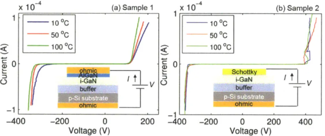
2.3.1 Vertical I-V and CV Characterization * Device Fabrication Sample 1 i-GaN Sample 2 Al-Schottky i-GaN
Figure 2-3. Cross-section scanning-electron-microscope (SEM) image of the wafer used in the study and schematics of two samples prepared for the electrical characterization.
The AlGaN/GaN-on-Si wafer used in this study has a 18 nm Alo.26Gao.74N barrier, -0.76
pm undoped GaN layer, ~0.86 pm graded AlGaN buffer and ~0.4 pm nucleation layer on a 4-inch 500-pm-thick Si( 111) substrate. The total epi-layer thickness is 2W0.1 ptm measured from the cross-section scan-electron-microscope (SEM) image in Figure 2-3. Two samples were prepared. Sample 1 has standard Ti/Al/Ni/Au alloyed ohmic contacts formed on the