HAL Id: tel-02378233
https://tel.archives-ouvertes.fr/tel-02378233
Submitted on 25 Nov 2019
HAL is a multi-disciplinary open access archive for the deposit and dissemination of sci-entific research documents, whether they are pub-lished or not. The documents may come from teaching and research institutions in France or abroad, or from public or private research centers.
L’archive ouverte pluridisciplinaire HAL, est destinée au dépôt et à la diffusion de documents scientifiques de niveau recherche, publiés ou non, émanant des établissements d’enseignement et de recherche français ou étrangers, des laboratoires publics ou privés.
investigation of 2D materials
Kevin Jaouen
To cite this version:
Kevin Jaouen. Backside absorbing layer microscopy : a new tool for the investigation of 2D materi-als. Chemical Physics [physics.chem-ph]. Université Paris Saclay (COmUE), 2019. English. �NNT : 2019SACLS296�. �tel-02378233�
Thèse
de
doctor
at
NNT
:
2019SA
CLS296
Backside Absorbing Layer Microscopy:
a new tool for the investigation of
2D materials
Thèse de doctorat de l’Université Paris-Saclay préparée à l’Université Paris-Sud Ecole doctorale n◦575 Electrical, Optical, Bio: Physics and Engineering (EOBE) Spécialité de doctorat : Physique Thèse présentée et soutenue à Saint-Aubin, le 16/10/2019, par
K
ÉVIN
JAOUEN
Composition du Jury : Anna Proust
Professeure, Sorbonne Université (IPCM) Présidente Emmanuel Maisonhaute
Professeur, Sorbonne Université (LISE) Rapporteur Erik Dujardin
Directeur de Recherche, CNRS (CEMES) Rapporteur Abdelkarim Ouerghi
Directeur de Recherche, CNRS (C2N) Examinateur Vincent Derycke
Chercheur, CEA (NIMBE, LICSEN) Directeur de thèse Renaud Cornut
In the PDF version of this manuscript, the section and figure numbers can be clicked to be redirected to the position of the section or figure.
The references in the text are linked to the reference section, which then provide a direct link to the online version at the editor website.
Some of the results were extracted from movies. These movies are accessible through the following links:
Movie-1: Optical monitoring of NBD dimer photodeposition on graphene oxide https://youtu.be/0xnhTLa5z8k
Movie-2: Electrografting of TBPFe on gold electrode by cyclic voltammetry https://youtu.be/n8jtcBx5UXk
Movie-3: Electrodeposition of copper on gold by chronoamperometry at -140 mV https://youtu.be/dnyClC8RHUA
Movie-4: Electrodeposition of copper on gold by chronoamperometry at -160 mV https://youtu.be/G7un94zrw0Y
Movie-5: Electrodeposition of copper on GO by chronoamperometry at 0 V https://youtu.be/SfoJLhkmGEA
Movie-6: Electrodeposition of copper on GO by cyclic voltammetry https://youtu.be/OXbbFoGmlUA
Movie-7: Electrodeposition of copper on ErGO by cyclic voltammetry https://youtu.be/73O8l_A01Ug
The publications related to this work are:
[1] K. Jaouen, R. Cornut, D. Ausserré, S. Campidelli, and V. Derycke, Ideal optical contrast for 2D material observation using bi-layer antireflection absorbing substrates,Nanoscale, 11 (13), 6129-6135,2019.http://dx.doi.org/10.1039/C8NR09983A
[2] K. Jaouen, F. Lebon, B. Jousselme, S. Campidelli, R. Cornut, and V. Derycke, Optical monitoring of diazonium electrografting on gold and graphene oxide using Backside Absorbing Layer Microscopy,submitted.
[3] S. Campidelli, R. Abou Khachfe, K. Jaouen, J. Monteiller, C. Amra, V. Derycke, and D. Ausserré, Backside absorbing layer microscopy: Watching graphene chemistry, Science Ad-vances, 3 (5), e1601724, 2017. http://dx.doi.org/10.1126/sciadv.1601724
[4] K. Jaouen, O. Henrotte, S. Campidelli, B. Jousselme, V. Derycke, and R. Cornut, Localized electrochemistry for the investigation and the modification of 2D materials, Applied Materials today, 8, 116-124, 2017. http://dx.doi.org/10.1016/j.apmt.2017.05.001
[5] O. Henrotte, T. Bottein, H. Casademont, K. Jaouen, T. Bourgeteau, S. Campidelli, V. Derycke, B. Jousselme, and R. Cornut, Electronic Transport of MoS2 Monolayered Flakes In-vestigated by Scanning Electrochemical Microscopy, Chemphyschem, 18 (19), 2777-2781, 2017. http://dx.doi.org/10.1002/cphc.201700343
Notations
2D 2 Dimensions
ACN Acetonitrile
AFM Atomic Force Microscopy
AR Anti Reflective
ARA Anti Reflective Absorbing
ARPES Angle-Resolved PhotoEmission Spectroscopy
BALM Backside Absorbing Layer Microscopy
CE Counter Electrode
CEA Commissariat à l’Énergie Atomique et aux énergies alternatives
CNT Carbon NanoTube
CV Cyclic Voltammetry
CVD Chemical Vapor Deposition
DMSO DiMethyl SulfOxide
EDL Electrical Double Layer
EIS Electrochemical Impedance Spectroscopy
EQCM Electrochemical Quartz Crystal Microbalance ErGO Electrochemically reduced Graphene Oxide
FQM Fluorescence Quenching Microscopy
FRET Fluorescence Resonance Energy Transfer
FTIR Fourrier-Transform InfraRed spectroscopy
FWHM Full Width-Half Maximum
GO Graphene Oxide
h-BN hexagonal Boron Nitride
HER Hydrogen Evolution Reaction
HOPG Highly Oriented Pyrolytic Graphite
HRTEM High-Resolution Transmission Electron Microscopy
IPA IsoPropyl Alcohol
IRM Interference Reflection optical Microscopy
ITO Indium Tin Oxide
KPFM Kelvin Prove Force Microscopy
LAO Local Anodic Oxidation
LICSEN Laboratoire Innovation, Chimie des Surfaces Et Nanosciences
MoS2 Molybdenum disulfide
MS Mass Spectroscopy
NA Numerical Aperture
NBDT 4-Nitrobenzenediazonium tetrafluoroborate
NIMBE Nanosciences et Innovation pour les Matériaux, la Biomédecine et l’Énergie
OCP Open Circuit Potential
ORR Oxygen Reduction Reaction
Ox Oxidant
PDMS Poly(dimethylsiloxane)
PIMI Polarization parameter Indirect Microscopic Imaging
PMMA Poly(methyl methacrylate)
QRCE Quasi Counter Reference Electrode
qSTORM quenching Stochastic Optical Reconstruction Microscopy
RE Reference Electrode
Red Reductant
rGO reduced Graphene Oxide
SAM Self-Assembled Monolayer
SECCM Scanning ElectroChemical Cell Microscopy
SECM Scanning ElectroChemical Microscopy
SEM Scanning Electron Microscopy
SERS Surface-Enhanced Raman Spectroscopy
SHG Second Harmonic Generation
SNOM Scanning Near-field Optical Microscopy
SPEM Scanning PhotoElectron Microscopy
SPM Scanning Probe Microscopy
STED Stimulated Emission Depletion Microscopy
STM Scanning Tunneling Microscopy
STS Scanning Tunneling Spectroscopy
TBAP Tetrabutylammonium hexafluorophosphate
TBPFe Tris-bipyridine Iron (III)
TEM Transmisson Electron Microscopy
TEPL Tip-Enhanced PhotoLuminescence
TERS Tip-Enhanced Raman Spectroscopy
THG Third Harmonic Generation
THz TDS TeraHertz Time-Domain Spectroscopy TIRF Total Internal Reflection Fluorescence
TMD Transition Metal Dichalcogenide
UPD Under Potential Deposition
UV Ultra-Violet
WE Working Electrode
WS2 Tungsten disulfide
XPS X-ray Photoelectron Spectroscopy
Contents
Notations I
Contents IV
Introduction 1
I State of the art for local study of 2D materials 5
I.1 Observation of 2D materials . . . 5
I.2 Structural characterization . . . 8
I.3 Optical and electronic properties characterization . . . 11
I.4 Chemical reactivity characterization . . . 14
I.5 Electrochemical properties characterization . . . 16
I.6 Summary and outlook . . . 20
II Backside Absorbing Layer Microscopy 23 II.1 BALM principle . . . 23
II.1.1 Anti-reflective coating principle . . . 24
II.1.2 Transparent anti-reflective layers . . . 26
II.1.3 Absorbing anti-reflective layer . . . 27
II.1.4 BALM configuration . . . 29
II.2 Status of BALM developments at the beginning of this work . . . 32
II.2.1 Observation of Graphene Oxide . . . 32
II.2.2 Discrimination between GO and rGO . . . 33
II.2.3 Adsorption of nanoparticles on rGO . . . 34
II.2.4 Adsorption of pyrene on GO . . . 35
II.2.5 First conclusions on the status of BALM at the beginning of this work . . . 36
II.3.1 Gold thickness . . . 37
II.3.2 Refractive index . . . 39
II.3.3 Wavelength . . . 40
II.4 Improving BALM and adding new functionalities . . . 47
II.4.1 In situ controlled deposition of molecules . . . 48
II.4.2 Sub-nm vertical resolution . . . 51
II.4.3 Guidelines for a 2ndARA layer selection . . . 52
II.4.4 GO contrast during the deposition . . . 53
II.4.5 Contrast enhancement with conventional 2ndlayer materials . . 55
II.5 Conclusions on Chapter II . . . 57
III Combining BALM and electrochemistry 59 III.1 Electrochemistry of ultrathin gold . . . 60
III.1.1 Electrochemical window of thin gold . . . 61
III.1.2 Impact of UV-ozone on gold . . . 62
III.1.3 Optical changes during basic electrochemical methods . . . 66
III.1.4 Impact of charge transfer on optical changes . . . 72
III.2 Electrochemical reduction of graphene oxide . . . 73
III.3 Electrografting of diazonium salts . . . 76
III.3.1 Comparison between BALM and EQCM . . . 77
III.3.2 Grafting at gold step edges . . . 80
III.3.3 Electrografting on 2D materials . . . 82
III.4 Copper electrodeposition . . . 88
III.4.1 Copper on gold . . . 89
III.4.2 Copper intercalation in graphene oxide . . . 92
III.5 Conclusions on Chapter III . . . 98
Conclusions & future directions 101 Experimental section 107 Slide manufacturing . . . 107
Synthesis and transfer of 2D materials . . . 109
Set-up and programs . . . 112
References 117
Introduction
Optical microscopy is a simple yet powerful characterization tool which notably allowed the first observation of graphene despite its ultimate single-atom thickness.
Soon after graphene, other 2D materials were discovered or synthesized with the same key role of optical microscopy techniques. 2D materials present a large spectrum of interesting properties (optical, electrical, chemical, mechanical, etc.) and are expected to contribute in many fields of applications. But their nanoscale size makes them espe-cially difficult to characterize. 2D materials are heterogeneous (edges, defects, single-layer vs. multisingle-layers, etc.) and they also present a large dispersion of their properties depending on the synthesis, transfer and aging conditions. For some applications, the material heterogeneity can be the reason of its outstanding properties. As an example, some defects and the layer edges in graphene or MoS2 are responsible for some of their attractive catalytic properties. Being able to probe locally the properties of 2D ma-terials is key to understand the structure-properties relations and is a prerequisite for the design of efficient devices based on materials with perfectly controlled structures.
At present, most of the techniques for local study of 2D materials are based on electron microscopy and scanning probe techniques, whereas the use of wide-field microscopy techniques is still mostly limited to the initial step of the studies (to locate the mate-rial flakes and estimate their thickness). Nevertheless, the discovery of graphene was only possible thanks to an optical microscope. Graphene was deposited on a special substrate having anti-reflective properties which made few layers graphene observ-able. Since then, enhanced optical microscopy techniques using this principle were improved, optimized and applied to 2D materials.
Recently, D. Ausserré from IMMM (CNRS and Maine University) introduced a new type of microscopy technique based on a special type of anti-reflective coatings, light absorbing materials, associated with the inverted microscope observation geometry (so that light comes from the glass side). This contrast-enhanced optical microscopy
technique is named Backside Absorbing Layer Microscopy (BALM). It is particularly adapted to the study of ultrathin materials both in air and in liquids and its geometry allows its combination with an electrochemical setup.
In this context, the objective of this thesis is to evaluate the potential of the BALM technique in order to study in situ the local properties (optical, chemical and electrochemical) of 2D materials, without using a scanning probe.
The manuscript is organized as follows:
In a first chapter, the different techniques used to investigate the local properties of 2D materials are reviewed. A particular attention is given to the measurement scale, to the in situ studies (i.e. techniques able to follow a phenomenon directly where and when it takes place) and to the techniques providing local information without scanning a probe.
Chapter 2 introduces the principles of anti-reflective coatings in optical microscopy and the way they produce contrast-enhanced images of 2D materials. The specificities of BALM are described and compared with those of conventional anti-reflection tech-niques. The status of the BALM technique at the beginning of this thesis is presented. Then several new experiments are presented and showed different ways to improve the anti-reflective conditions for the visualization of 2D materials. The investigation of molecular layer deposition dynamics notably shows the extreme sensitivity of BALM for such measurements. The contribution of multilayers anti-reflective coatings to in-crease the contrast during the observation of 2D materials, and the new functionalities they bring to the BALM set-up are then showcased.
Chapter 3 presents the combination of BALM with electrochemistry. It first shows the influence of basic electrochemistry experiments on the optical signal. In particular, it shows how the changes in the electrochemical double-layer (EDL) during a voltamme-try experiment lead to a measurable optical signal. Then, three studies coupling BALM and electrochemistry are detailed: first, the electrochemical reduction of graphene ox-ide is performed and optically monitored in situ. Then, the dynamic of diazonium salts electrografting is investigated at the local scale on gold electrodes, graphene oxide (GO) and reduced graphene oxide (rGO). Finally, the electrodeposition of copper is studied on gold, GO and rGO. The influence of the reduction state of GO on interlayer intercalation processes is notably studied.
Introduction
In a concluding chapter, the main achievements of this work are first summarized and used to analyse the main assets and limitations of the technique. Then, further devel-opments of the BALM microscopy and its combination with complementary techniques are discussed.
Chapter I
State of the art for local
study of 2D materials
This chapter reviews the different techniques to locally study and characterize 2D ma-terials. Optical techniques and local-electrochemistry techniques are more specifically emphasized. The choice was made to avoid a generic introduction on the 2D materi-als themselves, which are the subject of many comprehensive review articles. [6–11] Concentrating on the instrumental aspects of their study is more directly related to the core of the work and helps highlighting the associated challenges.
I.1
Observation of 2D materials
The discovery of graphene, [12] relied on two techniques, optical microscopy and Atomic Force Microscopy (AFM). The latter was essential in order to determine the number of atomic layers stacked within the aggregates produced by mechanical exfo-liation of graphite. It led to the first characterization of single-layer graphene sheets. To do so, it was also coupled to Scanning Electron Microscopy (SEM) for imaging the field-effect devices. Since then, these three techniques remained predominant as a first characterization step in most studies. AFM and SEM for 2D material observation will not be described hereafter as it is already extensively done in the literature. [13]
The crucial role that optical microscopy played in the field of 2D materials, from its very beginning, is of special importance in the context of this thesis. Indeed, the fact that graphene was not discovered sooner was well explained by Geim and Novoselov in their first review article about graphene in 2007 ("The rise of graphene" [6]):
"The problem is that graphene crystallites left on a substrate are extremely rare and hidden in a ’haystack’ of thousands of thick (graphite) flakes. So, even if one were deliberately searching for graphene by using modern tech-niques for studying atomically thin materials, it would be impossible to find those several micrometre-size crystallites dispersed over, typically, a 1-cm2 area. For example, scanning-probe microscopy has too low throughput to search for graphene, whereas scanning electron microscopy is unsuitable because of the absence of clear signatures for the number of atomic layers."
The innovative approach of the 2010 Noble Prize laureates was linked to the use of an optical microscope in a configuration capable of making few-layer graphene visible. This simple full-field microscope drastically reduces the time-effort to find interesting areas having as little stacked graphene layers as possible. Then AFM could be used on these areas to identify unambiguously single-layer graphene at the edges of the thinnest stacks. An example of a graphene deposition observed with an optical micro-scope is shown in Fig. I.1.a. [12] It first shows the chaos obtained after the deposition of graphene by mechanical exfoliation of graphite (the so-called scotch-tape method). On this image, the thickness of several flakes was measured by AFM and compared to their visibility. Few-layer graphene flakes as thin as 2 nm were observable using this fast optical technique.
The ultrathin material is visible because it was deposited on a special substrate which reflects very little light. This substrate is an oxidized silicon wafer with a precisely controlled SiO2thickness of 300 nm. Thanks to destructive interferences, this dielectric layer acts as an anti-reflective coating which provides contrast-enhanced. A deeper analysis of this type of anti-reflective substrates is presented in chapter II (section II.1). Since the discovery of graphene, this type of substrates have been improved and are routinely used for all types of 2D materials. [14, 17–21] An example of a single-layer Graphene Oxide flake deposited on silicon covered with 70 nm of Si3N4/Si is presented in Fig. I.1.b. [14]
Beside this interference based optical microscopy technique, which is still one of the most used techniques to locate 2D materials on surfaces, many other techniques were developed for the observation of single-layer materials. Two main optical techniques are notably employed: ellipsometry imaging and fluorescence quenching microscopy (FQM). The first one uses the modification of the polarization of the light reflected or transmitted by a material deposited on a surface. It was used to image many 2D
ma-I.1 Observation of 2D materials
Figure I.1: Optical microscopy techniques to image 2D materials. (a) Original first
observation of graphene in 2004 by optical reflection microscopy on a 300 nm SiO2/Si substrate, reprinted with permission from [12], (b) optimized imaging of Graphene
Ox-ide (GO) (∼ 100 µm large) on 70 nm Si3N4/Si substrate, reprinted with permission from [14], (c) ellipsometry imaging of graphene, reprinted with permission from [15],
(d) Fluorescence Quenching Microscopy (FQM) imaging of MoS2, reprinted with
per-mission from [16].
terials. [15, 22, 23] An example is shown in Fig. I.1.c in the case of graphene. [15] This technique uses the same substrate as for the first graphene observation (300 nm of SiO2 on Si). The second technique (fluorescence quenching microscopy) is based on the fact that graphene and other 2D materials are efficient fluorescence quenchers of nearby dye molecules. The difference of fluorescence between the substrate and the deposited 2D materials produces contrasted images, [16, 24, 25] as presented in Fig. I.1.d. [16] It was demonstrated to be efficient on any substrate. [26, 27] With the recent progress in super-resolution fluorescence microscopy, graphene was imaged by a combination of Fluorescence Resonance Energy Transfer (FRET) and Stimulated Emission Depletion Microscopy (STED). [28] Lately, graphene oxide was also imaged
using quenched Stochastic Optical Reconstruction Microscopy (qSTORM) with a res-olution of 16 nm. [29]
The development of high-throughput techniques was also driven by the necessity to characterize centimeter-scale graphene samples for future industrial applications. The goal is to develop inline measurement techniques for the structural characterization of 2D materials during their mass production. In this respect, optical techniques have remarkable assets in terms of versatility and speed.
I.2
Structural characterization
The first structural information usually needed after the synthesis is the number of stacked layers, the film continuity, the presence of cracks, etc. To get access to this, optical microscopy techniques were thoroughly applied. They were especially used to correlate the visibility of the flakes with the number of stacked layers as notably reviewed by Bing and co-workers in 2018. [30]. A machine-learning strategy was even applied to the optical identification of 2D materials. [31] All the techniques discussed above are able to observe single-layer materials as well as the continuity of the film. For centimeter-scale analysis, ellipsometry using only one adjustable parameter was performed on graphene and led to fast characterizations on various substrates. [32]
However, cracks and wrinkles are not always visible. To my knowledge, fluorescence quenching microscopy is the only optical technique which was used to quantify specif-ically the density of cracks in graphene. [33] But other types of enhanced microscopy configurations were also used to observe other types of defects. Dark-field microscopy is one of them, as it is very sensitive to small refractive index variations. It was in particular used to image graphene grain boundaries as shown in Fig. I.2.a. [34–36] Originally used in biology to study cell-substrate interactions, Interference Reflection Microscopy (IRM) was repurposed to image graphene on transparent substrates. [37] It allows the fast and label-free visualization of single-layers presenting defects, as pre-sented in Fig. I.2.b. The substrate can be made of polymers; therefore the technique was used to probe in situ the graphene cracks propagation under mechanical strain, as shown in Fig. I.2.c-d. The mechanical properties of 2D materials are out of the scope of this work and were already described in the literature. [38–40] Yet, it is interesting to note that many studies have also used TEM, SEM or optical microscopy to observe in situ crack propagation, exfoliation, bending, etc. [37, 41–44]
I.2 Structural characterization
Figure I.2: Optical techniques to observe defects in 2D materials. (a) Dark-field
microscopy, reprinted with permission from [36],(b) Interference Reflection Microscopy
(IRM), (c-d) in situ IRM images of graphene under uniaxial strain. Scale bars: 5 µm.
Reprinted with permission from [37].
Another way to reveal structural characteristics is to use indirect strategies. Different approaches were employed and combined to optical microscopy. Grain boundaries were selectively etched to create trenches which were then easily observable by mi-croscopy. [45–50] It was also demonstrated that rhodamine B (a fluorescent dye) is selectively adsorbed at graphene edges. Then the reacted grain boundaries were imaged using fluorescence microscopy. [51] Wrinkles and grain boundaries can also be highlighted by the deposition of gold nanoparticles along them. [52] Another sim-ilar approach using water micro-droplets was investigated to increase the contrast of graphene flakes. [53] Crystal orientation and grain boundaries were evidenced using liquid crystals which orientation depends on the underlying 2D material. [54–58] The orientation of CVD-grown MoS2 on graphene or WS2 was also used to determine the crystal orientation of the 2D materials and locate their grain boundaries. [59]
The optical techniques used so far have a lateral resolution limited by diffraction (except fluorescence quenching microscopy but high-resolution studies using these techniques are scarce). To our knowledge, the only super-resolution microscopy, not based on dye molecules and applied to 2D materials is the Polarization parameter Indirect Micro-scopic Imaging (PIMI). [60] This technique uses the indirect optical wave parameters obtained with the modulation of polarization to produce contrasted images. It was used to visualize graphene defects with sub-100 nm lateral-resolution.
For higher resolution characterization, the use of Transmission Electron Microscope (TEM) or Scanning Tunneling Microscope (STM) is well-established. They both allow the structural characterization of 2D materials down to the atomic scale. TEM imaging of 2D materials is a wide research field in itself which has been increasingly important in the last decade with the rise of aberration-corrected and low-energy TEM. It has
been used to observe 2D materials lattices, [61–63] defects, [64–66] crystalline phases and their orientations, [67, 68] chemical doping, [69] etc. TEM and STM are the only techniques able to visualize 2D materials at the atomic scale, therefore their uses is of critical importance to understand their properties. Particularly, TEM is getting even more popular with the development of new generation sample holders able to apply in situ different stimuli: mechanical, thermal, electrical, optical, magnetic and even in liquid or gas environments. The nanoscale characterization and manipulation of 2D materials using TEM is notably reviewed in [70] and [71] with a particular focus on the most recent and most advanced in situ techniques.
Last but not least, the structural characterization of 2D materials by the previous meth-ods is almost always coupled to AFM and/or Raman microscopy, which provide com-plementary information. As discussed previously, AFM is key to determine the number of stacked layers. But it is also commonly used to visualize defects like wrinkles and cracks. Soon after the first observation of single-layer graphene with AFM, Raman spectroscopy was shown to allow imaging graphene flakes using a scanning confocal setup. [72] It was demonstrated that Raman is sensitive to the number of layers and to their defects. Therefore, this technique has become one of the most extensively used for quality characterization of single-layer 2D materials.
Raman spectroscopy is typically mounted on a confocal microscope for high-resolution characterization and imaging of 2D materials but the development of wide-field Raman imaging allowed faster visualization. [73] With the rise of plasmonic research, Raman spectroscopy has been improved in two ways. First, 2D materials like graphene were used to produce Surface-Enhanced Raman Scattering (SERS), which improves the sensitivity of the technique. [74–77] Then, Tip-Enhanced Raman Spectroscopy (TERS) was found to be capable of imaging defects in graphene with an even better sensitivity and resolution than confocal Raman microscopy. [78, 79] It uses confined surface plas-mon at the tip of a scanning probe to increase Raman signals. Therefore, the resolution is mainly defined by the immediate volume surrounding the tip and is typically around 10 nm [80] but it can reach sub-nm resolution under ideal conditions. [81] TERS is so sensitive that it can even probe single molecules. [82]
I.3 Optical and electronic properties characterization
I.3
Optical and electronic properties
char-acterization
Optical properties
The first optical characterization which is generally performed on materials is absor-bance spectroscopy. This is especially difficult for few atoms thick materials and light transmittance of single-layer graphene was experimentally determined four years af-ter the initial discovery. [83] Then few techniques were deployed to probe the local transmittance of other 2D materials. Confocal absorption spectral imaging was used to increase the resolution of the spectral analysis. [84] Lately, optical fibers were used to reduce the size of the light spot of a classic microscope with two different con-figurations. First, when the optical fiber is on the backside of the sample (it thus needs a transparent substrate), the technique is named hyperspectral imaging. [85] Second, when it is on top of the sample, it is named micro-reflectance and transmit-tance spectroscopy. [86] They both present absorbance spectra of TMDs with different thicknesses and the resolution is determined by the diameter of the optical fiber (but is still limited by diffraction).
Then the complex refractive index of materials is mainly extracted using optical re-flectance microscopy and ellipsometry. To do so, the spectra are fitted using models incorporating the precise thickness of the layer (mainly extracted by AFM). Many stud-ies extracting the complex refractive index using these two techniques are reported in the literature. [87–97] Few other techniques were used to image and extract optical constants. First, quantitative phase microscopy which is based on the use of quadri-wave lateral shearing interferometry. [98] The special camera used in the set-up is capable of mapping both the intensity and wavefront profiles of a light beam passing through the material. Then, picometrology was also demonstrated. [99] It is based on interferometry (which measures the changes in reflection amplitude) but on a spinning disk in order to measure the phase shift at 2D materials edges.
One of the main techniques to probe the optical properties of 2D materials locally is photoluminescence. The characterization of 2D materials using photoluminescence has been reviewed by Jie and co-workers in 2018. [100]. In most cases, it is combined with Raman spectroscopy to measure the quality of the flakes. And like Raman, it is highly sensitive to defects therefore it can be used to visualize grain boundaries
Figure I.3: Comparison of the observation of MoS2 monolayers using different optical spectroscopy techniques. (a) Raman, (b) photoluminescence, (c) Second
Harmonic Generation (SHG) microscopy, (d) Third Harmonic Generation (THG)
mi-croscopy. Scale bars: 10 µm. Reprinted with permission from [107].
and defects. [101–107] The resolution was mainly improved using Scanning Near-field Optical Microscopy (SNOM) with "Campanile" nano-optical probe. Resolution down to 60 nm was obtained. [108–111] As for Raman spectroscopy, the photoluminescence signal is also enhanced at a tip therefore Tip Enhanced PhotoLuminescence (TEPL) has been successfully used for 2D materials characterization. [112, 113]
Other optical effects were used to study the local properties of 2D materials. For ex-ample, polarized optical microscopy was applied to black phosphorus as it presents anisotropic properties, [114] or to 1T’- 2H MoTe2. [115] Second Harmonic Generation (SHG) was showcased in TMDs. This nonlinear optical effect is based on the combi-nation of two photons of the same energy, which produce one photon with twice the energy when they interact within a material. It is highly sensitive to edges and grain boundaries. [115–118] Third Harmonic Generation (THG) was also demonstrated in 2D materials and its sensitivity to grain boundaries is higher than for SHG. [107] A compar-ison of Raman, photoluminescence, SHG and THG in the case of MoS2 is presented in Fig. I.3. [107]
Optical properties are directly related to electronic properties therefore both character-izations are ideally performed on the materials for a better comprehension.
Electronic properties
For the characterization of the band structure (specifically the valence band), Angle-Resolved PhotoEmission Spectroscopy (ARPES) is well-established. Its resolution is limited by the size of the beam but recent years have seen the development of micro-and nano-ARPES. Mapping the electronic properties of 2D materials is now possible. The use of ARPES on 2D materials was notably reviewed by Mo and co-workers in
I.3 Optical and electronic properties characterization
Figure I.4: Evidence of edge state conductance of MoS2 by the MIM technique.
In this technique, the microwave signal strikes on the surface and some is reflected by the sample, then the output signal is measured and related to the local resistance and capacitance of the sample. In this experiment, the local conductance was presented at different bias of a MoS2 field-effect transistor. Reprinted with permission from [124].
2017 [119] and a focus on spatially resolved ARPES for 2D materials was reviewed by Cattelan and co-workers the following year. [120]
For the spatial mapping of band structures, Scanning Tunneling Spectroscopy (STS) is suited. Combined with STM for the topography, local tunneling I(V) characteristics pro-vide information on the band gap and surface states. It was for example used to probe the band structure at the edge of MoS2. [121] The influence of defects and boundaries on the electronic properties using the different STM techniques was reviewed by Hus and co-workers in 2017. [122]
Among the most widely used techniques for the analysis of 2D materials electronic properties, one finds several AFM-related techniques. In addition to the classical to-pography imaging mode, several other AFM-based modes were developed. The dif-ferent methods used for local electrical characterization using scanning probe tech-niques were reviewed in details this year. [123] These AFM related techtech-niques (current-sensing AFM, Electrostatic Force Microscopy, Kelvin Probe Force Microscopy, etc.) provide extensive information on surface potential distribution, local conductivity, etc. at the nanoscale.
From the above mentioned studies, one can note that operando (i.e. in an operat-ing device configuration) analysis of electronic properties are limited. One example is the contribution of edge conductivity in MoS2 field-effect transistors studied by Mi-crowave Impedance Microscopy (MIM), as presented in Fig. I.4. [124] Other examples concern Kelvin Probe Force Microscopy (KPFM) studies on operating graphene, MoS2 and van der Waals heterostructures devices. [125–128] One striking technique relies on photoluminescence to image local current flow. Graphene was deposited on a
di-amond substrate containing N-V centers. Depending on the local charge density in bias graphene, the photoluminescence of these N-V centers is more or less quenched therefore the photoluminescence microscopy indirectly maps the charge density in op-erating devices. [129]
For the future industrial production of high-quality graphene, being able to probe the electrical conductivity over large areas is important. To do so, the use of movable four point probes or dry laser lithography is common but it requires physical contacts which may damage graphene. For non-contact mapping, TeraHertz Time-Domain Spectroscopy (THz TDS) is being developed. It consists in the measurement of the absorption of terahertz radiation across the 2D material flakes (MIM is one of these techniques). A comparison of these three techniques is provided in Ref. [130].
Finally, Cornut and co-workers (at CEA-Licsen) previously used local electrochemical techniques to probe the conductivity of different 2D materials. The mapping of electrical conductivity was investigated with Scanning ElectroChemical Microscopy (SECM) cou-pled to numerical modeling. It was performed on Graphene Oxide (GO), [131] reduced Graphene Oxide (rGO) [132] and MoS2. [5] Further explanations on local electrochem-ical methods are given in section I.5.
I.4
Chemical reactivity characterization
The most common combination of techniques for the local study of 2D materials chem-ical reactivity is Raman, photoluminescence and STM/AFM.
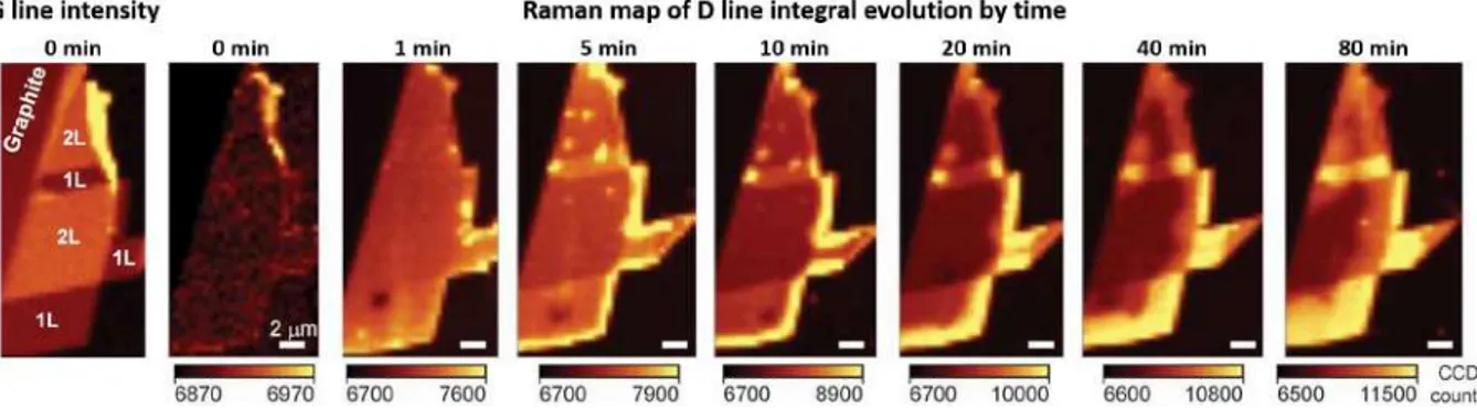
As described above, Raman and photoluminescence microscopy are able to image single-layers with high-resolution (for tip-enhanced versions) but at first they are spec-troscopy techniques. They can investigate small changes in the quality or environment of 2D materials, therefore they have been thoroughly used coupled to STM/AFM topo-logical information to probe the chemical reactivity of 2D materials. [133–144] A pro-totypical example of these studies is the functionalization of graphene by diazonium chemistry. The dynamic of the spontaneous chemical bonding process was extracted by Raman microscopy and it is presented in Fig. I.5. It is also important to note that the dynamic of graphene oxide photo-reduction was investigated using photoluminescence and absorption/emission microscopy. [145, 146]
I.4 Chemical reactivity characterization
Figure I.5: Local dynamic of graphene functionalization followed by Raman map-ping. Reprinted with permission from [142].
Raman was also coupled to Scanning PhotoElectron Microscopy (SPEM, or Spatially Resolved X-ray Photoelectron Spectroscopy) in order to map the quantity of diazo-nium molecules on graphene with a lateral resolution of 500 nm. [144] With the same goal, Mass Spectrometry (MS) techniques were employed using a local ionization beam. [147–149] XPS and MS also provide information on the type of molecules at 2D materials surfaces.
SNOM techniques previously discussed like TERS, TEPL and "Companile" probe are not limited to the visible range. Infrared was used and lead to nano-FTIR with enhanced chemical sensitivity. [150, 151]
At the atomic scale, STM was used to probe molecule adsorption and molecular or-ganisation on 2D materials. [133, 152, 153] And HRTEM was used to investigate phase transition and intercalation processes. [154–156] It has to be noticed that the interca-lation of alkali metals is TMDs was studied in situ by several groups. [157–159]
Of course AFM techniques are also widely used to probe local chemical reactivity. The topography can provide information on the layer thickness which depends on the functionalization. Most of the time, adding molecules on 2D materials modifies their electrical conductivity; therefore THz microscopy and conducting AFM were used to measure the dynamics of chemical reactions. [136, 160]
I.5
Electrochemical properties
characteri-zation
This part was the subject of a review by our team in 2017 and I was deeply involved in its redaction. [4] In the following, a summary of this review is first provided. Then a focus on the most recent studies that were published in and after 2017 is proposed.
The electrochemistry of 2D materials is of particular interest for energy conversion and storage applications. [161–164] Among others, graphite is used as anode electrode material in lithium-ion batteries. The issue with the study of 2D materials electrochem-ical properties is that the global efficiency of the system largely depends on inhomo-geneity or imperfections (such as edges, defect sites or upon folding and stacking). Understanding how these features influence the performances is challenging from a characterization point of view. But defects can also be turned into an advantage since their precise control could improve the devices.
The most common way to correlate the electrochemical properties of 2D materials with local information is to perform standard electrochemistry on samples with precise knowledge of the defects under investigation. But this requires other techniques to characterize the samples first such as AFM, SEM, Raman, etc. and other unknown or unobservable parameters may have a significant influence on the results.
Another approach has been developed with the rise of scanning probe microscopy techniques. Several groups developed new SPM techniques to probe local electro-chemistry. These techniques use different probes such as a scanning microelectrode (Scanning ElectroChemical Microscopy, SECM), a functional AFM cantilever, a scan-ning pipette (Scanscan-ning ElectroChemical Cell Microscopy, SECCM) or a confined mi-crodroplet, as presented in Fig. I.6. Depending on the scanning conditions, local in-formation can be obtained and plotted as electrochemical maps. The opposite is also possible as local modifications of 2D materials are possible using the same probes.
In [4], we first introduced the different local probe techniques that can be used to per-form localized electrochemical investigations of 2D materials. The techniques can be separated in two classes: in the first one, a sized-controlled electrode is scanned over the surface (SECM or AFM-SECM); in the second one, the measurement is confined in a microdroplet (SECCM or Microdroplet Cell). Both, the working electrode and the substrate potentials are controllable using a bipotentiostat.
I.5 Electrochemical properties characterization
Figure I.6: Presentation of the different probe techniques to perform local-ized electrochemistry. (a) Scanning ElectroChemical Microscopy (SECM), (b)
AFM-SECM,(c) Scanning ElectroChemical Cell Microscopy (SECCM), and (d) Microdroplet
cell. WE: WorkingElectrode, CE: Counter Electrode, RE: Reference Electrode, and QCRE: Quasi Counter Reference Electrode. The green triangle represents a piece of 2D material under study. [4]
Then, we presented the studies in which localized electrochemistry experiments are used to evaluate some key properties of 2D materials. For example, electronic con-ductivity (as discussed in I.3), ionic and molecular transport can be investigated using these techniques as well as charge transfers at surfaces using redox mediators.
Finally, we focused on contributions related to material modifications (electrochemical functionalization, etching, etc.), which allow modulating the properties in a spatially controlled manner. This field is mainly driven by conducting AFM, notably for the fabri-cation of graphene nanoribbons by Local Anodic Oxidation (LAO) [165–167] or for the local reducion of graphene oxide. [168, 169] Only few studies present the local electro-chemical functionalization of 2D materials. [169, 170]
At the end of 2016, the field was rapidly growing but most of the reported studies fo-cused on graphene. The most typical characterization concerned the evaluation of the kinetic constants associated to simple charge transfers, which is a basic electro-chemical process to characterize. The studies were mostly based on scanning probe microscopy with the associated drawbacks: it is difficult to locate areas of interest and
the small selected area under study may not be completely representative of the whole surface; it is very slow; the probe itself may impact the result; etc. Nevertheless, with the development of new 2D materials showing interesting properties for electrocatal-ysis, [171] localized electrochemistry should have a key role in order to better under-stand 2D materials electrochemical properties. A way to improve the characterization could be the combination of local electrochemistry with other microscopy techniques.
Since 2017
The study of the electrochemical properties of graphene continued but the investigation of other 2D materials increased more significantly, especially for TMDs which present interesting electrocatalytic properties. The field is now mainly driven by the group of Pr. P. Unwin at Warwick. This group notably improved drastically the SECCM technique and is intensively using it to study materials at the nanoscale. They reviewed their progress in a 2019 article. [172]
Simple charge transfer at the basal plane or at the edges of Highly Oriented Pyrolytic Graphite (which serves as a model for graphene) is still studied by SECCM, [173, 174] as well as electron transfers at MoS2 by SECM. [175]
Studies of the electrocatalytic properties have rapidly progressed in particular with TMDs in the case of the Hydrogen Evolution Reaction (HER). MoS2 is particularly investigated to sort out the relative catalytic properties of edges, defects, crystalline phases and basal plane. [176, 177] To do so, SECM and SECCM were used. It has to be pointed out that SECCM recently allowed the video-rate electrochemical map-ping of HER at MoS2. [177] Graphene and h-BN were also studied for HER using SECCM. [178, 179] However graphene materials are mostly investigated for the Oxy-gen Reduction Reaction (ORR), which is the limiting reaction in hydroOxy-gen fuel cells. Nitrogen or metal doped graphene were studied by SECM in order to show the influ-ence of doping on the electrocatalytical properties. [180, 181]
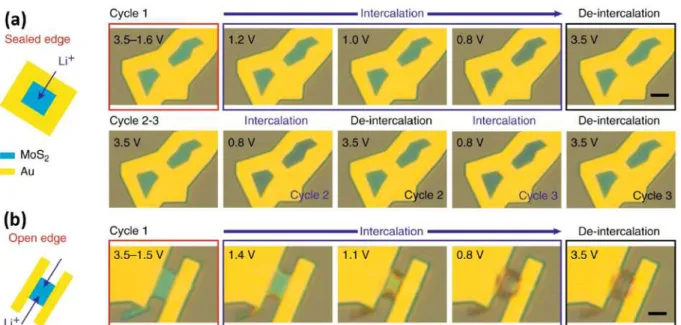
Similar to the Microdroplet Cell technique, a masking method has arisen. The 2D materials and the substrate are covered with a polymer resist and then a hole in this coating is produced using lithography. Therefore, only the selected hole contributes to the electrochemical reactions. HER at MoS2 was investigated using this technique. [182, 183] The same approach was performed on MoS2 but for the intercalation of ions. [184] It was shown that lithium and sodium can intercalate through the basal plane
I.5 Electrochemical properties characterization
Figure I.7: In situ optical images of Li intercalation in MoS2. (a) Through the
top surface, (b) through open edges. Scale bars: 5 µm. Reprinted with permission
from [184].
while potassium can only intercalate by the edges. The control over the intercalation of lithium is notably improved (reversibility and stability) when lithium intercalates through the top surface, as presented in Fig. I.7. The intercalation was followed by in situ Raman spectroscopy. Raman was also coupled to SECM in order to probe the redox activity of graphene. [185]
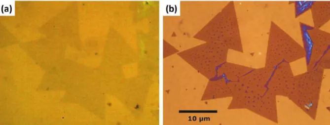
Interestingly, the intercalation in MoS2 induces a modification of the optical properties, therefore, in 2018, it was followed in situ by optical reflection microscopy as shown in Fig. I.7. [184] The electro-ablation of TMDs was also investigated in 2018 by optical reflection microscopy and the dynamic of the process was showcased. [186] Recently, the Interference Reflection Microscopy (IRM) and the fluorescence microscopy tech-niques were used to study the oxidation and reduction of graphene. [187, 188] The local dynamics are reported at video-rate and a mechanism is suggested. Examples of IRM images of graphene during the oxidation and reduction process are presented in Fig. I.8.
Finally, the work on the local modification of 2D materials continued using Local Anodic Oxidation with the goal of improving the resolution. [189–191] Graphene nanoribbons are still studied as well as TMDs. [190,192] To our knowledge, no studies were reported for the local electrochemical functionalization of single-layer 2D materials since 2017.
Figure I.8: In situ Interference Reflection Microscopy (IRM) images of electro-chemical oxidation and reduction of monolayer graphene. (a-c) Oxidation at 1.6
V,(d-e) reduction at 0 V. Scale bars: 5 µm. Reprinted with permission from [187].
Within the two last years, the field has extented both through the study of new materi-als and through the improvement of the characterization techniques. The local electro-chemical studies are no more limited to SECM related techniques. Other approaches have emerged and the combination of electrochemistry at 2D materials surfaces with complementary techniques like Raman spectroscopy is spreading. Optical microscopy starts being used to observe in situ the modification of 2D materials under electro-chemical reactions, in particular in the case of intercalation.
I.6
Summary and outlook
High-sensitivity optical microscopy has been the missing key for the emergence of 2D materials as it allowed the fast visualization and localization of single-layer flakes. Since 2004 many techniques have been used to image and characterize 2D materials providing critical information for the development of the field.
Reflection optical microscopy and ellipsometry imaging are two important optical mi-croscopy techniques not only capable of imaging but also used to extract the optical properties of 2D materials. The complex refractive index extracted using these meth-ods critically depends on the thickness measurement of the 2D material which is not always reliable by AFM. [193] This error combined with the imperfections of the models induce large differences between studies in the reported results (as will be detailed in Chapter II for MoS2). The third main optical technique is Fluorescence Quench-ing Microscopy, which is interestQuench-ing and very powerful because its lateral resolution is not limited by diffraction (when used in a super-resolution configuration). Furthermore, it was proven to be usable on any substrates. The drawback is that it requires dye molecules at the surface, which is hardly compatible with chemistry-oriented studies.
I.6 Summary and outlook
For high resolution imaging, TEM and STM are the only two techniques achieving atomic resolution. Especially, TEM has been increasingly used within the last decade with huge technological improvements. It can combine atomic resolution with elemen-tal/chemical information. With the development of environmental TEM and sample holders applying external stimuli, in situ studies start to come out. For now, in situ TEM is still limited to simple reactions and imaging in liquid is still in its infancy.
AFM is ideal for structural characterization and is almost always performed in 2D ma-terial studies. Its use is not limited to topography but variants of the AFM technique have been applied to 2D materials to probe notably the local electrical properties, the reactivity (combined with TERS) and the electrochemical properties. These techniques are also becoming faster with technological improvements, therefore in situ and video-rate investigation of 2D materials are expected to appear soon. The main issue for the study of 2D materials is that the thickness measurement accuracy highly depends on the measurement and quality of the flake. [193] The extracted properties are also probed at a very local scale and one must be careful that the probed area is fully rep-resentative of the system since homogeneity at a large scale is sometimes difficult to guaranty (and reproduce) with nanomaterial deposition techniques.
Optical spectroscopy techniques like Raman, Photoluminescence and FTIR are exten-sively used as they are capable of imaging 2D materials ant their defects. They are highly sensitive to chemical changes in the environment of the flakes which makes them suitable for chemical sensing. The resolution is enhanced by near-field mi-croscopy at a tip (TERS or TEPL) or using a "Campanile" probe (nano-PL).
For local electrochemical characterization, SECM and related techniques are promi-nent. Lately, SECCM was improved and the electrochemical mapping speed reached video-rate with a pixel size of 1 µm2. The use of lithography to give access only to the surface of interest is increasing as it uses well-known processes and the electro-chemistry is performed using standard equipment. The drawback is that at some point, the surface is entirely covered with a polymer and some residues can be left on the developed surface. Such residues are known to impact significantly the electrical prop-erties of 2D materials and a similar impact is thus expected for the electrochemical properties.
Most of the time several of these techniques are combined in order to provide comple-mentary information at different scales. As they all have their own pros and cons, it is
important to cross-check the data for highly accurate characterization. The ideal would be to combine the techniques in the same experiment like topological AFM with TERS for chemical sensing at the local scale. Examples of such strategy were developed lately: a combination of electrochemistry with AFM-TERS was demonstrated for the first time in 2019 by the group of P. Van Duyne (Northwestern University) in order to map the redox activity on an electrode surface in situ and at the sub-µm scale. [194] There is no doubt that such combination will be applied to 2D materials very soon.
Except for some specific TEM studies or some studies of mechanical properties, the local characterization of 2D materials is either in situ but not local or local but not in situ (i.e. based on before/after type of comparisons). Only very few studies combine in situ operation with local information. This is especially the case for electrochemical properties for which in situ studies are mainly performed on electrode materials. [195, 196] Furthermore, the catalytic or energy storage capacities are highly dependent on defects which are still important features in 2D materials. [197] So there is a need for additional local techniques to probe the impact of defects, edges, etc. that can be combined with in situ analysis.
Almost all the techniques described above are based on scanning probe microscopy. Wide-field techniques are mostly limited to the static observation of 2D materials. It is in this context that this thesis presents an optical microscopy technique to investigate in situ chemical and electrochemical reactions at single-layer 2D material surfaces.
Chapter II
Backside Absorbing Layer
Microscopy
In the first chapter, the different ways to observe and analyze the local properties of 2D materials were presented. From this we can see that there is a lack of wide-field, in situ / real-time techniques and especially to study their local electrochemical prop-erties. In this chapter, we introduce a recently developed enhanced optical microscopy technique and determine its performances for the observation of 2D materials as well as for monitoring chemical reactions.
II.1
BALM principle
Optical microscopy was invented in the 17th century and had a tremendous impact on society, as it allowed scientists to observe a world they could only imagine before. Conventional optical microscopy, the oldest and simplest type of microscopy, is present in every research labs. The last century saw the emergence of many new types of enhanced optical microscopy techniques with the aim of improving, among others, the two main criteria of performance: lateral resolution and contrast.
Lateral resolution represents the minimum distance (d) between two distinguishable points. The resolution of conventional optical microscopes is limited by diffraction and was fully described by Ernst Abbe in 1873. [198] He notably introduced the following equation quantifying diffraction-limited microscopy:
d = λ
with λ, the light wavelength and NA, the Numerical Aperture (depending on the objec-tive quality and provided by the manufacturer). The BALM technique being based on a conventional microscope, its lateral resolution is also limited by diffraction. The specific lateral resolution of our set-up will be briefly described later for clarity.
Indeed, the main goal of BALM is to improve the second criterion: contrast. It charac-terizes the intensity or color distribution within an image. It is important to understand that an image with a poor contrast can only be slightly improved by post-treatments and that this manipulation can distort the results. In this thesis, we consider the con-trast resulting from instrumental considerations and not the one resulting from post-treatments.
Contrast can be defined in several ways. In this work it was decided to use the definition proposed by Michelson, [199] which is particularly suited for an object deposited on a support. This Michelson-contrast is calculated using the following equation:
C = Iobject – Isupport
Iobject + Isupport (II.2)
By looking at this equation, there are two ways of maximizing the contrast. First, Isupport = 0 (observing bright object on a dark background), and second, Iobject= 0 (dark object of a bright background), so that |C| = 1. From an experimental point of view, it is easier to control the intensity of the support. This solution is experimented by everyone observing the sky: the stars are only visible when the sky is dark (Isupport = 0) and not during daytime. This type of contrast-enhanced images is also produced by the darkfield microscopy technique.
BALM is a new type of contrast-enhanced optical microscopy technique, which comes from the use of specific substrates with Isupport close to zero.
II.1.1
Anti-reflective coating principle
When light crosses an interface between two transparent media with different optical properties, one part is transmitted and the other part is reflected. The ratio is quanti-fied by Fresnel equations [200, 201] and in the special case of normal incidence, the reflected light is calculated by the following equation:
R = ni – ne ni + ne 2 (II.3)
II.1 BALM principle
with niand ne, the refractive index respectively of the incident and emergent media. For
example, the light crossing perpendicularly a window is reflected at 4% by the air/glass interface and around 7.7% considering the two interfaces. This is due to the difference between the refractive index of air (n = 1) and glass (n = 1.5). An optical microscope has two most common configurations, in transmission and in reflection. In the later case, the light comes from the objective, is reflected by the object/support, and the image is captured by the same objective.
In this configuration, there is a well-known solution in order to obtain Isupport = 0: Anti-Reflective (AR) coatings. These coatings have many industrial applications, [202–204] with the most known being on glasses. As for windows, the air/glass interface reflects light and this coating allows people to see the eyes of the persons wearing glasses without seeing in addition their own reflection.
These coatings are based on the control of the light reflected by the interfaces. To do so, a new layer with precisely-selected optical properties and thickness is added on glass, as shown in Fig. II.1. This coating adds one interface and thus, the incident light is first partially reflected by the {incident medium/coating layer} interface and partially transmitted. The light transmitted in the coating layer is then partially reflected by the {coating layer/emergent medium} interface. The layer properties (refractive index and thickness) are chosen so that, the light reflected by the two interfaces interfere destructively, resulting in no reflected light (Isupport = 0).
Figure II.2: Effect of a transparent coating on the reflection of the air/glass inter-face (simulation results for λ = 450 nm, nair = 1, nglass = 1.5, and light perpendicular to the interface).
II.1.2
Transparent anti-reflective layers
Most of the time, the anti-reflective layer is made of a transparent material as it was discussed in the bibliography part I. The transparent AR coatings have been studied for decades and the two equations, derived from Fresnel equations, governing the choice of the perfect AR layer are well-known:
nAR2 = nine (II.4)
Ensuring that the same amount of light is reflected by the two interfaces of the AR layer. And:
eAR = λ
4nAR (II.5)
Defining the AR coating thickness, eAR, as a function of nARand λ. It ensures that the phase difference between the reflected light from the front and back surfaces generates destructive interferences.
The respective impact of nARand eARwithin these two equations can be illustrated us-ing simple simulations (Comsol-based model usus-ing the Fresnel equations). The model includes a single AR layer between two semi-infinite media (air and glass). Then the refractive index of the transparent AR layer was parametrized and the reflection was plotted against AR thickness, as shown in Fig. II.2. The refractive indexes chosen were typical of polymer materials used for conventional AR coatings. It can be observed that for nAR < nglass, eq: II.4 is approached and therefore it decreases the reflected light.
II.1 BALM principle
All the curves reach a minimum reflection at λ/4nAR, that is why the single AR coatings are called quarter-wave layers.
Theoretically the perfect coating can give zero reflection but equation II.4 shows that the optimum refractive index for the AR coating layer is √nine so nAR = 1.22 for the
air/glass interface. Unfortunately, materials with n < 1.3 are not usual therefore the anti-reflective conditions can only be approached using a single transparent AR layer.
However, single transparent layer AR coatings allow a good approximation of the anti-reflective conditions and are cheap to produce. AR layers were also improved by real-izing multilayer AR coatings. [204]
II.1.3
Absorbing anti-reflective layer
Absorbing materials like metals are not commonly used for AR purpose because of their well-known high reflectivity, which is conversely put at profit to produce mirrors. Nevertheless, few systems using absorbing coatings are described in the literature. They are useful when light transmission is not important for the AR coating. They can even produce thinner and cheaper AR layers. [204–211]
From an analytical point of view, only few treatments were developped. [205] It was previously demonstrated that in a classical single-layer configuration, the AR layer must be thicker than λ/4, [201, 212, 213] therefore the light cannot pass through these highly absorbing layers and consequently there is no output signal.
That was until Dominique Ausserré from IMMM (Université du Maine) and co-workers demonstrated in 2014 the use of a single Anti-Reflective Absorbing (ARA) layer at the air/glass interface. [214] When a material absorbs light, its refractive index is a com-plex refractive index, nARA– jkARA, k being the extinction coefficient of the material. In the publication, [214] they derived Fresnel equations by taking into account the complex refractive index of the ARA layer and by making the approximation of a strongly absorb-ing material (high k). A full demonstration is provided in the supplementary information section of [3] and the following equations were obtained for ideal AR conditions:
nARA2– kARA2 = nine (II.6)
eARA' λ 4π
(ni – ne)
Figure II.3: Gold ARA layer at the air/glass interface. Schematics with (a) light
com-ing from the air, (b) light coming from the glass. Comsol calculations of (c) reflection
and absorption in the two configurations,(d) zoom on the reflection of a very thin gold
layer.
The most important information extracted from these equations is that, in order to ob-tain a real thickness value (eARA) in eq: II.7, ni has to be higher than ne. This means
that light has to come from the higher refractive index medium.
As for transparent AR coatings, simple simulations can be used to evaluate the amount of reflected light in such configuration. The reflection and the absorption of the air/glass interface are compared when a gold layer is used as ARA layer. The difference be-tween light coming from the air (classical configuration) and from the glass (inverted microscope) are compared. Schematics and results are presented in Fig. II.3.
The light absorption and reflection of the classic configuration (light coming from the air in a classical set-up), are plotted in black. The addition of the gold layer increases the reflected light as its thickness grow and it behaves as a mirror. In regard to eq: II.7, the
II.1 BALM principle
Figure II.4: BALM configuration. (a) Schematic, (b-c) anti-reflective properties of the
BALM configuration and effect of the addition of a material at the imaging surface.
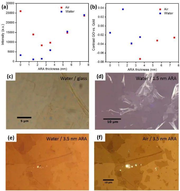
AR properties emerge only with the inverted configuration (light coming from the glass), as it is plotted in red. For really thin gold layer, the reflected light initially decreases and reaches a minimum around 5 nm. Meanwhile, the absorption is around 20% so contrarily to the previous publications the AR properties are not lost by the presence of a highly absorbing material.
D. Ausserré and co-workers named this new combination (absorbing AR layer + obser-vation from the glass side): the Backside Absorbing Layer Microscopy (BALM).
II.1.4
BALM configuration
A schematic of the BALM set-up is presented in Fig. II.4. Since light has to come from the higher refractive index material, BALM uses a simple inverted microscope on top of which is placed a glass coverslip covered with an ultrathin gold ARA coating. The layer thickness depends on the emergent medium and is typically around 5 nm in air or 2 nm in water. The microscope is placed in reflection configuration therefore, light is sent through the objective, reflected by the object/support, and the image is created by the same objective. Finally, in order to obtain the best possible images, the microscope is equipped with a high numerical aperture oil immersion objective (NA = 1.4). The immersion oil is here to create a continuous refractive index medium between the objective and the glass. This prevents unwanted reflections and also increases the resolution of the objective by increasing its numerical aperture.
All of this combined, creates a "near-ARA" coating with Isupport close to 0 and when a 2D material, or any other material leading to a modification of refractive index, is deposited on top, the microscope produces contrast-enhanced images as represented by the two schematics of Fig. II.4.b,c.
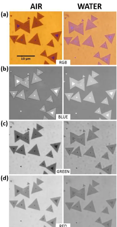
The contrast enhancement of the BALM configuration will be studied in details but is first simply exemplified in Fig. II.5. MoS2 flakes were deposited on a gold BALM sup-port and the sample was imaged with a classic microscope (light coming from the air side) (a) and with the BALM microscope (light coming from the glass side) (b). The re-sult is that the monolayer domains are barely distinguishable from the surrounding gold surface with our classic microscope whereas the BALM microscope clearly reveals ad-ditional details of the sample. Note that better images of MoS2than the one reported in (a) can be obtained with conventional microscopes when the substrate is, for example, Si/SiO2 but ultrathin gold on glass is a chalenging substrate for microscopy in reflec-tion. In any case, reported MoS2 images in conventional microscopy configurations do not reach the level of contrast provided by BALM, as shown in Fig. II.5.b. The impact of the ARA layer will be further shown in Fig. II.13 and Fig. II.14.
Looking at Fig. II.5.b, it is also important to note that the MoS2 appears darker than the background. When explaining the BALM principle, it was assumed that the ARA thickness would correspond to the minimum of the curve in Fig. II.3.c so that any addi-tional material could only increase the amount of reflected light. In practice, addiaddi-tional material can also bring the system closer to the minimum of reflection case so that depending on the ARA thickness and type of observed object, materials can appear brighter or darker than the background. This will be detailed later (notably in Fig. II.15).
In terms of lateral resolution, BALM is equipped with a high Numerical Aperture objec-tive (NA = 1.4), therefore, when used at wavelength of λ = 450 nm, the set-up could theoretically achieve a lateral resolution of d = 160 nm. In practice, the actual lateral
Figure II.5: Representation of contrast enhancement by the BALM microscope.
Images of MoS2 flakes deposited on a gold BALM substrate(0.5 nm Cr + 3 nm Au),(a)
II.1 BALM principle
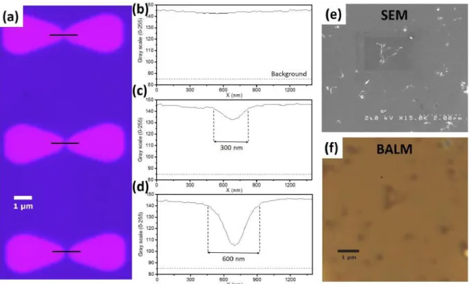
Figure II.6: Experimental resolution limit of the BALM set-up. (a) BALM image of
chromium triangles on gold with increasing separation, (b,c,d) associated gray scale
profiles. Carbon nanotubes imaged with(e) SEM and (f) BALM.
resolution is closer to 300 nm as illustrated in Fig. II.6. This figure displays BALM im-ages of micro-fabricated pairs of chromium triangles (thickness 2 nm) deposited above a gold thin film. Triangles separated by different distances are produced by e-beam lithography. Chromium patterns separated by ∼ 300 nm are distinguishable in the line profile (c), even though the color dip becomes shallow.
It is important to note that lateral resolution does not correspond to the minimal size of individual objects that can be observed. Individual particles smaller than 160 nm can readily be observed but pairs of such objects cannot be distinguished from individual objects. This is exemplified in Fig. II.6.e-f, Carbon NanoTubes (CNT) around 50 nm in diameter are deposited on a BALM substrate and then imaged by SEM and BALM. The BALM technique clearly detects particles smaller than the diffraction limit. Other experiments able to distinguished nano-objects using the BALM microscope were also performed: in our group for Fe3O4nanoparticles [3] and in 2018 at Itodys (Paris-Diderot University) with silver nanoparticles [215, 216] and at CRPP (CNRS Bordeaux) with single-wall CNTs (see figure S5 in the Supporting Information of Ref. [217]).
![Figure I.2: Optical techniques to observe defects in 2D materials. (a) Dark-field microscopy, reprinted with permission from [36], (b) Interference Reflection Microscopy (IRM), (c-d) in situ IRM images of graphene under uniaxial strain](https://thumb-eu.123doks.com/thumbv2/123doknet/12718094.356540/18.892.114.786.107.269/techniques-materials-microscopy-reprinted-permission-interference-reflection-microscopy.webp)