Configurable Byte-wide HDLC Controller Supporting IP over SONET
by
Daniel T. Lee
Submitted to the Department of Electrical Engineering and Computer Science in Partial Fulfillment of the Requirements for the Degree of
Master of Engineering in Electrical Engineering and Computer Science
at the Massachusetts Institute of Technology May 8, 1998
Copyright 1998 Daniel T. Lee. All rights reserved.
The author hereby grants to M.I.T. permission to reproduce and distribute publicly paper and electronic copies of this thesis
and to grant others the right to do so.
Author
Department of Electrical Engineering and Computer Science May 8, 1998 Certified by John T. Wroclawski Thesis Supervisor 27 Accepted by I AA Chairmaj,
<S.ACHU ETTS INSTITijUT
Arthur C. Smith Department Committee on Graduate Theses
JUL 141998
LIBRARIESConfigurable Byte-wide HDLC Controller
Supporting IP over SONET
by
Daniel Tzonglin Lee
Submitted to the Department of Electrical Engineering and Computer Science on March 19, 1998, in partial fulfillment of the
requirements for the degree of
Master of Engineering in Electrical Engineering and Computer Science
Abstract
Increasing demand for high bandwidth networks has prompted the use of fiber optics as the next step for physical medium. We develop the data-link layer, in hardware, required to transmit IP packets over SONET. In particular, we design the byte-wide HDLC controller that frames PPP-encapsulated network-layer packets, as described in RFC 1662, "PPP in HDLC-like Framing." Targeted for a Xilinx, Inc. XC4000XL-series FPGA, the design will interface with PMC-Sierra, Inc. S/UNI-Plus or S/UNI-622 SONET framers and will include the appropriate interface logic. Furthermore, a few additional options are designed into the chip. We also reveal that a design with a higher degree of modularity will outperform one with a lower degree.
Thesis Supervisor: John T. Wroclawski Title: Research Scientist
for cpet. Thanks.
Acknowledgements
I would like to thank the following people for their assistance and support during the development
of this thesis:
John Wroclawski, my thesis advisor, for the opportunity to do this thesis and the belief that I could pull this off.
The real and virtual, former and current inhabitants of NE43-537: Rena Yang, Wenjia Fang, Rob
Cheng, Pedro Zayas, Elliot Schwartz, Dina Katabi, Atanu Mukherjee, and those really neat puzzles that Wenjia owns. We were not always the paragons of productivity, but our conversations have helped me
understand more about networking.
Friends and family: for helping me get through some tough times and being there when I needed
them since the beginning.
Last, but certainly not least: Janet Wu, for her assistance in VHDL and digital design and
A BSTR A C T ... 3
CHAPTER 1: INTRODUCTION... 10
1.1 B ACKGROUND ... 10
1.1.1 Point-to-Point Protocol in IP over SONET... ... 11
1.2 G O A L S ... ... 12
1.3 THESIS OVERVIEW... ... ... 13
CHAPTER 2 : TOOLKIT AND DESIGN FLOW ... 14
2.1 DESIGN FLOW ... 14
2.2 DESIGN ENTRY ISSUES ... 16
2.2.1 V H D L L im itations ... ... 17
2.3 VERIFICATION ISSUES ... 17
2.4 IMPLEMENTATION (PLACE-AND-ROUTE) ISSUES... 18
CHAPTER 3 : DESIGN SPECIFICATION ... 19
3.1 FUNCTIONAL SPECIFICATION ... 19
3.1.1 Basic Design Functions (HDLC specification) ... 19
3.1.2 Extended Design Functions ... 20
3.2 INTERFACE SPECIFICATIONS ... ... 20
3.2.1 T ransm it Side ... 2 1 3.2.2 Receive Side ... ... ... 21
CHAPTER 4 : DESIGN IMPLEMENTATION ... 23
4.1 TRANSM IT SIDE ... 24
4 .1.1 H eader G enerator... 25
4.1.2 Trailer G enerator ... 28
4.1.3 Byte Stuffer ... 30
4.1.4 Transmit Frame Check Sequence (FCS) Generator ... 32
4.1.5 SONET Interface Logic (Transmit side) ... ... 34
4.2 RECEIVE SIDE ... 36
4.2.1 Byte De-stuffer ... ... 37
4.2.2 Byte Counter ... 39
4.2.3 Receive Frame Check Sequence (FCS) Generator and Comparator... 42
4.2.4 SONET Interface Logic (Receive side) ... ... 43
CHAPTER 5 : TESTING ... ... 45
5.1 FUNCTIONAL VERIFICATION ... 45
5.2 STATIC TIM ING ANALYSIS ... 46
CHAPTER 6 : RESULTS AND CONCLUSION ... 47
6.1 IMPLEMENTATION RESULTS ... 47
6.2 C ONCLUSIONS ... 47
APPENDIX A: CODE LISTING ... 49
Chapter
1
: Introduction
1.1 Background
Increasing demand for bandwidth from network applications, from conferencing to file transfers, motivate the development of faster networks supporting Internet Protocol (IP) traffic. One path is the
transmission of data over optical fiber. Fiber has very low bit-error rates and signal attenuation, and the
maximum theoretical bandwidth is measured in terabits per second.
The framing protocol for optical networks run by telephone companies is known as SONET
(Synchronous Optical Network) or SDH (Synchronous Digital Hierarchy), the technical difference between
them primarily in the frame header. The SONET/SDH framing process adds header information to outgoing data. The header is used for synchronization and control signals between peer SONET framers. Designed to reduce operation and equipment costs, yet provide transmission rates beyond copper, SONET
starts at about 52 Mbps (STS-1), while SDH starts at 156 Mbps (SDM-1). Higher rates are multiples of the
base rate, so STS-3 is 156 Mbps.
SONET framers map voice into a SONET frame, but they can also map data into a frame. Most
framers designed to transmit data map ATM (Asynchronous Transfer Mode) cells into the frame. ATM was designed to transport both voice and data, unifying the various telephone and cable networks, and operate over SONET [19]. To transmit IP packets over an ATM-SONET network, the IP packets are segmented and inserted into ATM cells, with some additional overhead via the AAL (ATM adaptation layer). Then, the ATM cells are mapped into the SONET frames as usual. If the goal is to just transfer IP packets, then the IP-ATM-SONET process may not be a good idea. ATM imposes a per-cell overhead of
at least 5 bytes for every 53 bytes, so the maximum bandwidth utilization is just over 90%. (AAL 3/4 adds
4 bytes of additional overhead, reducing utilization to 83%, but AAL 5 imposes no per-cell penalty.)
One alternative to increase bandwidth utilization of IP-over-ATM-over-SONET is to directly map
IP into SONET frames. Some bandwidth is saved and processing overhead is reduced by eliminating ATM.
1.1.1 Point-to-Point Protocol in IP over SONET
Substituting for data-link functionality, when ATM is taken out of the picture, is PPP (Point-to-Point Protocol). PPP multiplexes network-layer protocols through a 16-bit header.
Protocol Information (e.g. IP packet)
16 bits n bits
Figure 1-1: PPP encapsulated packet.
The 16-bit protocol field uniquely identifies what type of packet is in the information field. The
possibilities include IP, IPX (Novell), and PPP control packets (link control and network control), among
others, for link establishment. The values assigned to different protocols can be found in the "Assigned Numbers" RFC. While the header identifies the packet, framing, the process of adding a checksum and
headers and marking the space between packets, is still required.
This framing is provided by the HDLC protocol. Normally a bit-oriented protocol, HDLC maps a
network layer packet into a frame suitable to transmit over a physical layer like SONET. All bit-oriented HDLC-like protocols use the same frame format.
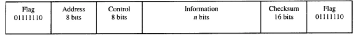
Flag Address Control Information Checksum Flag
01111110 8 bits 8 bits n bits 16 bits 01111110
Figure 1-2: Generic bit-oriented frame.
Flags are reserved values and mark inter-frame space; at least one flag sits between two
consecutive frames, and flags are transmitted when the connection is idle. Bit sequences in the data packet that might be misconstrued as control sequences (e.g. a flag field) are "stuffed," i.e. replaced with a different sequence that is deconstructed at the receiver, transparent to the network-layer protocol.
A byte-oriented version of HDLC very much looks like the bit-oriented HDLC. In the case of
PPP, the address and control fields have lost some functionality - the fields are fixed [17]. Byte-oriented
HDLC is specified for mapping PPP packets into SONET/SDH frames: no compression of the address and
Flag Address Control Protocol Information FCS Flag 01111110 11111111 00000011 16 bits (e.g. IP packet) 32 bits 01111110
n bits
Flag (inter-frame fill) or next Address
Figure 1-3: Byte-oriented HDLC frame, per RFC 1662. The protocol header of PPP is shown explicitly.
Instead of bit-stuffing, byte-oriented HDLC uses byte-stuffing to replace special characters in the frame. The HDLC protocol can be implemented in hardware, since its function set is not large. In
addition, a hardware controller should be faster than a software implementation, and CPU time processing the outgoing frame should be reduced. One possible network interface card (NIC) design using HDLC is
the following:
Figure 1-4: Top-level block diagram, showing one possible application of the HDLC controller.
The controller frames data from the PPP layer before transmitting it to the SONET/SDH framer. In the
receive path, the reverse is true.
1.2 Goals
In this thesis, a byte-oriented HDLC controller suitable for PPP over SONET at OC-3c (155
Mbps), per RFC 1662 and RFC 1619, will be designed, synthesized, and tested for behavior and timing. The design will be implemented using a field programmable gate array (XC4000-series) from Xilinx, Inc.
The controller will have the required logic to interface with a PMC-Sierra SONET framer, either the S/UNI-Plus or the S/UNI-622. In addition, the issue of modularity will be addressed, and we will show
how a design with many small modules outperforms one with few large modules.
1.3 Thesis Overview
In the next chapter, an overview of the design flow and the design tools (Xilinx Foundation) will
be given. Chapter 3 discusses the specifications of the design and the interfaces in detail. Chapter 4
describes the final implementation of the controller on a module-by-module basis; the verification of the
implementation is in chapter 5. Finally, chapter 6 reviews the performance results between a monolithic
Chapter 2
:
Toolkit and Desig n Flow
The design of this HDLC controller required the use of certain software tools. The Foundation
software, from Xilinx, Inc., provides a complete top-down solution, from design entry (VHDL and
schematic entry) to implementation (place-and-route) into a Xilinx FPGA (Field Programmable Gate Arrays), a device with an internal array of combinational logic blocks, registers, and interconnect resources.
How the various resources behave can be programmed into the device. The use of FPGAs makes sense,
since they are cheaper to build in low quantities versus custom ASICs, and they also can be
re-programmed. Mistakes can be fixed and design improvements can be implemented in the FPGA by simply
re-programming the device.
Associated with the toolkit is a design flow, starting with the determination of specifications and ending with the implementation of the design in a target FPGA. However, certain steps of the flow may change, depending on project requirements. We start by reviewing a design flow, then discussing issues
surrounding the design entry, verification, and implementation stages of the flow, in the context of the Foundation design tool.
2.1 Design Flow
The first step in the design flow is to understand what the design will do and where it belongs in the context of a larger design, like a network interface card. The functionality of the device can come from several places: from established standards and specifications like Internet standards documents and Request for Comments (RFCs); from algorithms, like the fast Fourier transform used in digital signal processing; or
from older designs that need to be revised and improved. The external interfaces of the device under
design depend on other devices and, sometimes, on performance criteria. This is especially true for bus
widths. The internal data bus of the device may be 32-bits wide, but additional logic will be required to
interface the device to an 8-bit device. When these issues are sorted out and the functions are partitioned
into modules, the next step is design entry.
Expressing a design requires at least one of the following, in increasing order of control over the
level. The method (or combination of methods) used depends on project objectives and constraints.
Typically, this includes what tools are available and the degree of optimization of area and/or speed. For example, a high performance design may require more work at the layout level, since added control over the implementation may be required. In our case, however, the main focus will be on design using VHDL.
Functional verification of individual modules and of the whole system of modules is closely
linked with design entry. After a module has been coded, but before synthesis, it is tested with unit or no
delay. Verification is done at both the module and system levels, checking modules' functionality as well
as their interfaces with respect to each other.
The next step in the flow is implementing the design in a target FPGA. This process actually
includes two steps: translation and place-and-route. The translation process converts the wires and gates in the netlist (from synthesis and/or schematics) into FPGA logic blocks, taking into consideration any
implementation constraints set by the user (pin placement, etc.). The blocks are optimized, and then the
process goes to place-and-route, or PAR. In PAR, the software attempts to find the optimal placement and connectivity of the logic blocks, taking into consideration net delays and any physical constraints imposed
by the user.
The last step in the design flow is to check that all signals meet worst-case timing requirements. The place-and-routed design gets worst-case timing information assigned to each logic element, including
logic blocks, buffers, and wires. Then, the simulator runs test vectors on the implemented design, revealing
worst-case timing paths.
Assuming the report files indicate the worst-case delays are within timing specifications, most signals will satisfy the requirements. Signals that do not may require returning to PAR for additional iterations or different user constraints, in order to squeeze extra performance from the design. Extremely poor results that do not respond to changes in PAR require re-evaluation and re-designing of the device.
Timing models of devices that meet the design's various external interfaces should be used, so a more
accurate representation of maximum delays can be created. The test vectors developed for functional
2.2 Design Entry
Issues
By designing in a hardware description language (HDL) instead of schematic entry or FPGA logic
block editing, we can take advantage of a much higher level of abstraction and leave the gate synthesis to a
software compiler. In addition, the behavior of the code can be easily understood. Code is also portable, so
the same code that works on one compiler in general should work with another. Compilers can also optimize logic expressions and state machines, saving some time and hassle.
A critical drawback to VHDL design is also the dependence on the compiler. [18] describes three
problems with VHDL. First, by using a compiler, the engineer forfeits gate-level control of the resulting circuit. Since compilers are algorithm-driven, the best one can usually do is to specify parameters of the algorithm, either area-optimal or a speed-optimal. The LogiBLOX (Foundation) optimizations are
device-specific, and move away somewhat from the idea of VHDL being a "high-level" language. Second, the
compiler output will likely not be the most efficient circuit, because, again, of limitations in synthesis algorithms. Finally, the result from one compiler may differ from another compiler.
On the other end of the spectrum, directly programming and routing logic blocks means having absolute control of the design and should give the best results in terms of utilization and performance. However, little is automated, so more work is required on the part of the designer. The logic equations are
created and optimized by hand, and, for large designs, this process may take an immense amount of time and is error-prone. Furthermore, small changes in the design, like adding a single logic block in a module, can affect the rest of the design in dramatic ways. In a worse case scenario, the entire device will require re-routing. Of the three techniques, logic block editing is the least obvious and portable method. What behavior the logic blocks and the routing represent is not obvious without a lot of study, and the design is
not compatible with an FPGA of different architecture or size.
Schematic entry lies somewhere between VHDL and layout. Schematics are easier to read and
understand than layout, yet offer more control over the final implementation than VHDL synthesis.
However, altering a schematic when an error is found can still be a tedious and time consuming task,
especially when the design starts to get big. Wires and gates will have to be drawn and re-drawn. Like
layout, the overall behavior of a schematic may not be intuitively obvious from quick observation.
like specialized clock or input/output buffers. (If the goal is to use device-specific elements, though, then
schematic entry is very useful, since all the elements will be instantiated as a graphic and can be easily included in the design.)
2.2.1 VHDL Limitations
Several caveats must be observed when using Foundation. First, the VHDL compiler and the
XACTstep place-and-route tool have some incompatibilities. In order to avoid some multiple-driver-per-line errors under XACTstep, the compiler optimization in the compiler must be turned off for any VHDL
module included in the design. Also, VHDL port names must be kept relatively short (about 8-10
characters or so), else the schematic tool truncates the name, confusing XACTstep. These kinds of
behavior are caused by net-naming problems between the compiler and the implementation tool. Second, large VHDL modules (in number of gates compiled) tend not to work well in terms of both area and speed.
In fact, the documentation recommends that VHDL modules compile to less than 4000 gates.
For Foundation, some additional benefits come from using VHDL. The compiler offers several
useful libraries that allow adders to be expressed as vector sums (e.g. c <= a + "00001") for readability. Foundation's LogiBLOX can also detect special logic structures in the VHDL code, such as RAM or
adders, and replace them with pre-optimized modules (LogiBLOX modules may also be instantiated directly in VHDL code). This optimization is device-specific to Xilinx FPGAs and can take advantage of
special architectural features of the FPGA family, such as dedicated carry logic.
2.3 Verification Issues
In functional verification, the Foundation logic simulator sets the delay to all elements to zero, though artificial delays can be built into the model via the after expression in VHDL. Test modules can be
written and hooked up to the design to ease testing. For example, said modules may be state machines that
output certain data and will respond to the design under test; however, they need to be compiled with the
rest of the design and must be removed prior to device fitting. Alternatively, command (or script) files
but can still ease testing. So far, no option was found in Foundation to use the test modules from functional verification in static timing analysis.
The testing strategy for the HDLC controller is to verify first each functional module individually, then check systems of modules. The controller design mostly uses state machines for the various modules.
Each state machine is tested by traversing every state and all state transitions. Other non-trivial modules,
like the FCS generators and the scrambler/de-scrambler, are compared to reference designs.
2.4
Implementation
(Place-and-route)
Issues
The implementation process in Foundation actually includes two steps: translation and place-and-route. The translation process converts the wires and gates in the netlist into FPGA logic blocks, taking
into consideration any implementation constraints set by the user (pin placement, etc.). The blocks are optimized, and then the process goes to place-and-route, or PAR. In PAR, the software attempts to find the
optimal placement and connectivity of the logic blocks, taking into consideration net delays and any physical constraints imposed by the user.
Foundation offers two additional options to PAR to improve results. One is re-entrant routing. Basically, this tells the PAR software, given the placement of the logic blocks, to re-route the design
additional times, keeping the best result. The other option is multi-pass PAR, where each "pass" uses a slightly different implementation, and the best ones are saved.
Chapter 3
: Design Specification
3.1
Functional Specification
3.1.1 Basic Design Functions (HDLC specification)
This design performs the basic functionality as specified in RFC 1619 and RFC 1662. The
specified base SONET data rate for PPP over SONET is OC-3, or about 155 Mbps. Since the design interface between the HDLC controller and the SONET framer is only 8 bits wide, the controller must be
able to sustain at least 19.5 MHz at its output.
When creating an HDLC frame, the controller takes a PPP packet from the PPP module, then it adds header the standard headers and appends the frame check sequence for the packet. Byte stuffing is
performed over the whole frame, including the header and FCS. Control bytes, Ox7D and Ox7E, found in the frame are replaced with the two byte sequence Ox7D Ox5D (0x7D) or Ox7D Ox5E (0x7E). The second byte in the sequence is the original byte XORed with 0x20. Finally, the byte stuffed frame is transmitted to the SONET framer.
When receiving data from the SONET module, the controller looks for frames among the
inter-frame spacing (flag bytes). Frames less than 6 bytes in length are ignored, since 6 bytes are just enough to
represent a valid HDLC frame (1 byte address, 1 byte control, 4 byte FCS, but no data). The incoming frame is also checked for errors via another FCS.
Byte de-stuffing continually replaces stuffed sequences by dropping the initial escape byte (0x7D), and the second byte, XORed by 0x20, is transmitted to the next module. Assuming the transmitter
performs byte stuffing correctly and no transmission errors occur, the receiver should not encounter
sequences Ox7D Ox7E or Ox7D Ox7D. Interestingly, at the receiver, [17] implicitly allows Ox7D 0x7D,
since any byte except Ox7E (which is always invalid) is XORed with 0x20. This leaves Ox7D Ox7E as the
only invalid sequence in byte-oriented HDLC. When the invalid sequence is detected, the Ox7E is assumed
to be the flag byte that marks the end of the current frame, and a stuffing error is signaled to the PPP layer
3.1.2 Extended Design Functions
Functions beyond the basic HDLC specifications include several options. First, the default
headers can be overridden, and the PPP module can provide its own address and control information. Second, special interface logic is required to interface the controller design to PMC-Sierra SONET framers.
The transmit side of the interface has a data scrambler, based on the x43+1 polynomial, while the receive
side has a module that de-scrambles the incoming data. The scrambler and de-scrambler can be
independently enabled or disabled. The use of the scrambler and de-scrambler is not specified in [15] but is
mentioned in both [11] and [13], which mentions it in the context of ATM transmission.
One particular feature of the PMC-Sierra framers is that if their transmit buffers contain less than one full ATM cell's worth of data, the framer automatically transmits an "idle" ATM cell. The
transmission of the idle cell will disrupt the correct processing by the receiver HDLC controller. For example, if an idle cell gets transmitted in the middle of an HDLC payload, then the receiver will assume the cell is part of the HDLC payload. Hence, the clock frequency of the HDLC controller must be
somewhat higher than the minimum required rate. The design, then, operates at speeds of at least 20 MHz, producing a data rate of 160 Mbps or above, roughly 4 Mbps above the SONET transmission rate. In turn,
the PPP buffers must be able to provide data fast enough not to starve the HDLC controller and,
consequently, the SONET framer. (The PPP layer could, for example, not signal a start of packet indicator
to the transmit HDLC until an entire packet has been loaded into the PPP buffers on the NIC.)
Received frames that have a byte stuffing error are not silently discarded as described in RFC 1662. They are instead transmitted normally to the PPP module but marked as having a stuffing error.
3.2 Interface Specifications
The HDLC controller design interfaces to two different devices: the SONET framer and the PPP
module (or some higher layer module). The PMC-Sierra application note describes the 8-bit interface
between the HDLC and the SONET module, and the signals are described below. The interface to the PPP
3.2.1 Transmit Side
The transmit interface between the PPP module and the controller consists of an 8 bit data path, a start of packet (SOP) indicator, a default fields (DF) signal, and a scrambler disable (NO_SCR). The PPP module starts a new transmission by raising SOP and presenting the data byte at the same time. Also, the
DF signal should be asserted or de-asserted for at least one clock cycle. Similarly, the end of a
transmission is indicated through presenting SOP low at the same time as the last data byte, so for a packet
of length n, the SOP signal is high for n-1 clock cycles. The NO_SCR signal can be asserted or de-asserted at any time. Asserting the signal immediately stops the scrambling function of the HDLC-SONET
interface, but no guarantees can be made that the receiver can determine when the scrambling stopped. When the SONET framer starts to run out of buffer space, it de-asserts transmit cell available
(TCA, active low), and both the HDLC and PPP modules must respond by holding their outputs for as long
as TCA remains de-asserted. TCA is used to gap the 20 MHz clock that drives the transmit sides of both the HDLC controller and the PPP module. The framer's internal transmit buffer requires an indicator for the start of an ATM cell; the HDLC controller must assert transmit start of cell (TSOC) every 54 bytes
transmitted (ATM cell size).
The PPP module and the HDLC controller are on the same (gapped) clock, so the controller
signals ready back to the PPP module. When ready is sampled low, the PPP module should not change its
data and SOP outputs. The design also generates a gapped clock from the 20 MHz reference, and the PPP module presents signals to the HDLC on this clock.
3.2.2 Receive Side
A byte stream from the SONET module is presented to the HDLC controller one byte at a time.
The receive SONET-HDLC interface uses a receive cell available (RCA) signal to gap a 20 MHz clock that drives only the receive side of the controller and the PPP module. (RCA and TCA are independent.)
In addition to the 8-bit data bus, the controller uses several other signals to indicate the condition
of the received frame. First, a receive SOP signal is used in the same way as the transmit version. Second,
S_ERR marks packets that have a stuffing error. Finally, if a packet has no stuffing errors or transmission errors, it is marked with GOOD_FCS.
Chapter 4
:
Design Implementation
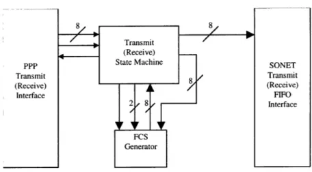
Two implementations were created. The original implementation has a single, monolithic state
machine each for the transmitter and receiver, while the final implementation has multiple, small state machines in a more modular design.
In the original implementation, the transmit state machine serves as header generator, trailer
generator, and byte stuffer, while the receive state machine integrated the byte de-stuffer and the byte counter. The result is state machines with 20 and 30 states.
8 8
Transmit (Receive)
ppp ] State Machine SONET
Transmit 8 Transmit (Receive) Z (Receive) Interface FIFO 2 8,, Interface FCS Generator
Figure 4-1: HDLC block diagram with monolithic state machine. The FCS generator is also different from the final implementation.
The figure illustrates the data flow and control signal directions for the transmit side, using a FCS generator that integrates a multiplexor controlled by the state machine. The receive side is very similar, except that the data paths are reversed. Other differences include a minor change in the FCS generator (no
multiplexor, but a comparator in the module replaces the 8-bit output with a single bit) and control signals
to the PPP interface. In the end, the original implementation did not meet the performance specifications
and required a very large FPGA. A different approach had to be taken.
A faster design of the HDLC controller, the one described detail in this chapter, takes advantage of
addition, they are all implemented using VHDL code and integrated using schematic entry, except where noted.
4.1
Transmit Side
The transmit side of the HDLC controller maps the PPP packet into an HDLC frame, then sends
the frame to a lower level device, the SONET framer. As previously described, the HDLC frame can be divided into three parts: header information, including the address and control fields; the PPP data
(minimum of two bytes); and a trailer, consisting of the frame check sequence (FCS) and at least one flag
byte to mark inter-frame space. This side of the controller provides the header and the trailer. Furthermore, byte stuffing is performed over the entire frame.
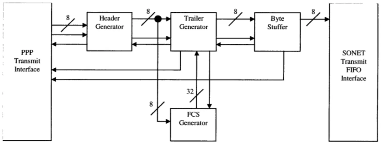
This implementation uses multiple modules to form the HDLC frame:
8 Header Trailer 8 Byte
Generator Generator Stuffer
PPP SONET
Transmit Transmit
Figure 4-2: Transmit side HDLC block diagram.
The header state machine interfaces with the PPP-layer device. Both the transmit HDLC controller and the
PPP transmit interface operate on the same clock, generated from the HDLC controller (see Section 4. 1.5 SONET Interface Logic, Transmit Side). The state machine normally transmits the default HDLC address
and control values (OxFF and 0x03, respectively), but that can be disabled, allowing the PPP layer to
bypass header generation (useful when PPP needs to use different address and control values). If no packet
needs to be transmitted, then the header generator state machine transmits flag bytes to the trailer generator
state machine. These bytes are not confused with packet data, because these bytes are not marked as such. The trailer module manages the FCS generator and transmits the FCS result. Normally, it
transmits bytes from the header module to th the PPP-layer . Both theader module indicates that no more
FCS for the current packet. When the header generator presents a byte not marked as packet data, the byte
is ignored and merely transmitted to the byte-stuffer, without modification or transmission to the FCS generator. At the conclusion of a frame, one flag byte is inserted into the byte stream. The next frame can
start immediately after the single flag byte.
The byte-stuffer examines data from the trailer generator. If the byte is marked as packet data,
then if it is either Ox7E or Ox7D it is stuffed into a two byte sequence (Ox7D Ox5E or Ox7D Ox5D,
respectively). Otherwise, the module ignores the byte and transmits it to the SONET interface. Typically, only inter-frame flag bytes are not marked as packet data and, therefore, not stuffed.
4.1.1
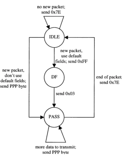
Header Generator
The transmit header generator (HG) determines what type of header information - the Address and Control fields of the HDLC frame - to include. Normally, the header generator provides the default values
for Address and Control (OxFF and 0x03, respectively). Alternative values can be used if the header generator is set to bypass mode.
no new packet; send Ox7E
IDLE
new packet, use default fields; send OxFF new packet,
don't use DF end of packet;
default fields; send Ox7E
send PPP byte
send 0x03
PASS
more data to transmit; send PPP byte
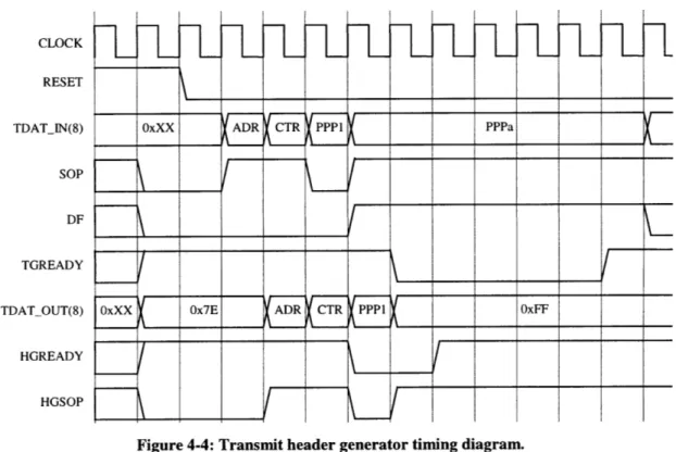
Figure 4-3: Transmit header generator state machine.
After reset, the module waits for the PPP layer to signal the start of a new packet, through the start
of packet (SOP) signal, asserted at the same time as the first byte of data. Depending on whether the HG is in header bypass mode or not, the next state is either DF or PASS. If the mode is selected (default fields asserted), then the first byte of data should be the HDLC address field, and the next state is PASS. Otherwise, the next state is DF. The PPP layer signals an end of packet condition by de-asserting SOP while presenting the last byte of the packet. Since only one signal is used to signal both start and end of a packet, the PPP layer must present at least two bytes. The first byte is presented with SOP asserted, the
second byte with SOP de-asserted.
The module uses a ready signal to indicate whether the PPP layer should present the next data
byte. If the PPP layer samples ready de-asserted, then the previous values of the PPP data byte, SOP, and
DF should be held until ready is re-asserted. The module de-asserts the signal when transmitting default
The HG sends its 8-bit output to both the transmit FCS module and the trailer generator. The HG
also generates a start of packet indicator for the trailer module. It is essentially a re-timed version of the
SOP signal generated by the PPP module.
Modules later in the data path, such as the trailer generator and byte stuffer, communicate with the
HG through their own ready signals. The HG holds its outputs when either module de-asserts their ready
signals.
CLOCK RESET
TDATIN(8) OxXX ADR CTR PPPPPPa
SOP
DF
TGREADY
TDATOUT(8) OxXX Ox7E ADR CTR PPPxFF
HGREADY
HGSOP
Figure 4-4: Transmit header generator timing diagram.
In the timing diagram, two packets are presented at the input port of the HDLC controller by the PPP module. The first packet, ADR-CTR-PPP1, shows a case where the default fields (signal DF) are not used, immediately followed by a packet using default fields. The trailer generator uses TGREADY to make the PPP device hold its current value on TDAT_IN and the HG to hold OxFF at its output. The byte
stuffer's ready signal (not shown) has a similar effect as TGREADY. The clock is actually a gapped clock
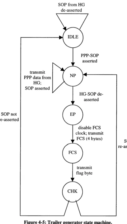
4.1.2 Trailer Generator
The trailer generator (TG) manages the transmit FCS generator through reset and clock enable
control signals. Furthermore, at the conclusion of a PPP packet, indicated by the HG de-asserting its SOP signal, the TG transmits the FCS and a flag byte to end the HDLC frame.
SOP from HG de-asserted SOP not re-asserted SOP re-asserted
Figure 4-5: Trailer generator state machine.
The default state is IDLE, where the HG and PPP modules are holding their SOP signal
stuffer. It also presets the FCS register. When the PPP module asserts SOP, the TG releases the preset signal to the FCS. This action is based on the PPP-SOP, because the FCS consumes data directly from the HG. Therefore, the preset signal must be de-asserted early. The TG remains in state NP, transmitting data
unchanged to the byte stuffer, as long as SOP is asserted.
When the HG presents the last byte of data, it also de-asserts its SOP, causing the TG state
machine to go from NP to EP. After that final byte gets transmitted, the state machine disables the FCS
clock, holding the value of the FCS register. Then, the TG takes the contents of the FCS register and transmits its complement over 4 clock cycles, one byte transmitted per clock, least significant byte first.
After state FCS, the state machine marks the end of the frame with a flag byte and checks for a
new packet (SOP asserted). If one is detected, then the next state is NP; the TG resets the FCS, and its next state is NG (as above). Otherwise, the next state is IDLE.
Since the TG cannot accept any data when transmitting the FCS, it uses two ready signals, one
each to the HG and the PPP device, to communicate when new data can be presented. The ready signal comes to the PPP device one state (clock) earlier than the one to the HG.
In any state, the TG does not transition to a new state and holds its output values when the byte
CLOCK RESET
TDATIN(8) OxXX Ox7E ADR CTR PPP1 OxF
PPPSOP
HGSOP
TDATOUT(8) OxXX x7E ADR CTR PPP1 FCSO FCS FCS2 FCS3 x7E
TGSOP
READY PPP
READY HG
FCS PRESET
FCSCLKEN
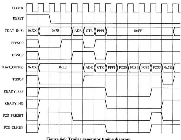
Figure 4-6: Trailer generator timing diagram.
The diagram above shows the same transaction as the one for the header generator. The two READY signals go either the PPP or the HG modules, depending on the suffix of the signal name.
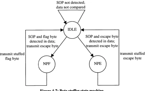
4.1.3 Byte Stuffer
At this point, the HDLC header and trailer, along with the frame payload, have been assembled. The next step is to apply byte stuffing over the whole frame, before transmission to the FIFO manager for the SONET framer. The byte stuffing mechanism in this HDLC controller only stuffs the flag (0x7E) and
escape (0x7D) bytes.
Under normal operation, the header generator transmits the flag byte during idle periods. Idle
periods are recognized through yet another start of packet signal, this time from the trailer generator.
Depending on the state of the SOP signal from the TG, the transmit byte stuffer (TBS) can ignore a data
SOP not detected;
transmit stuffed flag byte
transmit stuffed escape byte
Figure 4-7: Byte stuffer state machine.
While in the IDLE state, the state machine checks the condition of the SOP signal, sent from the trailer generator. If asserted, then the current data byte is compared to Ox7E and 0x7D. A match to Ox7E
sends the state machine to state NPF, while Ox7D (Escape) is transmitted to the FIFO manager. Similarly, a match to Ox7D makes the state machine transition to NPE, and Ox7D is also transmitted. At the next clock, the respective stuffed version (0x5E or Ox5D) gets transmitted, and the TBS returns to IDLE.
Since a single data byte can be transmitted as two bytes, the TBS needs a way to pause the TG,
HG, FCS generator, and PPP device, so no new data gets presented. A single ready signal is fed back to
the transmit modules, including the PPP device. When de-asserted, the modules hold their current outputs and do not change states.
CLOCK TDATIN(8) TGSOP TDATOUT(8) BSREADY
7
Ox' EL EF--
ADR1
CTR r 1Ox7E
F 7D-7DOx7E ADR CTR x7D 0x5E
Figure 4-8: Byte stuffer timing diagram.
LSO
,so
-L
ES:1
-IS2
-IL
E
C
I I I 1 I I i 1 IThe timing diagram shows an HDLC frame with payload Ox7E Ox7D. The first Ox7E in the timing requires one clock cycle to effect BSREADY, so the trailer generator presents the next byte, Ox7D.
This time, it holds Ox7D while the byte stuffer transmits the stuffed sequence Ox7D Ox5D.
4.1.4
Transmit Frame Check Sequence (FCS) Generator
Since the HDLC operates on a byte-wide data path, the transmit frame check sequence generator (TFCS) also needs to work on a byte-wide basis. An XOR tree was derived from Morse's article that
describes how CRCs work and the basis of a byte-wide CRC implementation.
clock reset enable
data from 8
HG / 32 bit
XOR 32 / FCS A 32/, contents of FCS
Tree reg. / register to TG
32/
clock
Figure 4-9: Diagram of FCS generator.
The tree comes from the linear feedback shift register (LFSR) implementation of the 32-bit CRC, where data are shifted bit-wise into the shift register with XORs between certain flip-flops. The XORs
correspond to the generator polynomial; in this case,
G(x) = x 32 +x 26 +x 2 3 +x 22 +x 16 x12 -x 11 -x 10 x8 +x 7 +x 5 +x 4 X2 +X +1
The LFSR contains the value of the FCS of all the bits shifted in since the last reset or preset, so if
Bit 31 30 29 28 27 26 25 24 23 22 21 20 19 18 17 16
R31 R30 R29 R28 R27 R26 R25 R24 R23 R22 R21 R20 R19 R18 R17 R16 Bit 15 14 13 12 11 10 9 8 7 6 5 4 3 2 1 0
R15R14R13R12R11 R10 R9 R8 R7 R6 R5 R4 R3 R2 R1 RO
Figure 4-10: Contents of the FCS register, just after preset and before any bits get shifted in. R31 through RO are the initial values of the FCS. In this case, they are all '1'. The highlighted bit
positions indicate the terms of the CRC polynomial.
Bit 31 30 29 28 27 26 25 24 23 22 21 20 19 18 17 16 TO R31 R30 R29 R28 R27 R26 R25 R24 R23 R22 R21 R20 R19 R18 R17 TO TO TO TO TO TO TO TO TO Bit 15 14 13 12 11 10 9 8 7 6 5 4 3 2 1 0 R16R15R14R13R12R11 R10 R9 R8 R7 R6 R5 R4 R3 R2 R1 TO TO TO TO
Figure 4-11: One bit of data has been shifted in. The LSB gets shifted out and XORed with the
message bit. The result (TO) is fed back to the register.
Bit 31 30 29 28 27 26 25 24 23 22 21 20 19 18 17 16 T1 TO R31 R30 R29 R28 R27 R26 R25 R24 R23 R22 R21 R20 R19 R18 T1 TO TO T1 TO TO T1 TO TO T1 TO TO TO T1 T1 T1 T1 T1 Bit 15 14 13 12 11 10 9 8 7 6 5 4 3 2 1 0 R17 R16 R15 R14 R13 R12 R11 R10 R9 R8 R7 R6 R5 R4 R3 R2 T1 TO T1 TO TO T1 TO T1
Figure 4-12: The register after the second shift.
Bit 31 30 29 28 27 26 25 24 23 22 21 20 19 18 17 16 T1 TO TO TO T1 TO TO TO R31 R30 R29 R28 R27 R26 R25 R24 T7 T1 T1 T4 T3 T1 T1 T2 T3 T2 T2 T3 T1 TO TO TO T6 T5 T5 T4 T2 T2 T4 T4 T3 T4 T4 T2 T1 T1 T2 T7 T6 T6 T5 T3 T3 T5 T6 T5 T5 T6 T3 T2 T3 T3 T7 T7 T4 T5 T7 T7 T6 T7 T7 T5 T4 T4 T4 T6 T6 T6 T5 T5 T7 T7 T6 Bit 15 14 13 12 11 10 9 8 7 6 5 4 3 2 1 0 R23 R22 R21 R20 R19 R18 R17 R16 R15 R14 R13 R12 R11 R10 R9 R8 T2 T1 TO TO T3 T2 T7 T1 TO T4 T1 TO T1 TO TO T2 T3 T2 T1 T4 T6 T5 T5 T3 T2 T2 T1 T3 T7 T6 T5 T7 T6 T4 T3 T5 T4 T7 T6
Figure 4-13: The final value of the register after a total of 8 shifts. The terms in each column are
XORed together to get the new value of the register bit. Duplicate terms have been removed from the chart.
Figures 2 through 5 use the same notation and are based on the derivation of the byte-wide implementation
of the 16 bit CRC in (Morse 86).
Figure 9 shows the contents of the FCS register immediately after preset, before any data has been
shifted in. For FCS calculations, the register is preset to OxFFFFFFFF. In Figure 10, the least significant
bit of the data gets shifted in. DO, the LSB of data, is XORed with RO, the 0th bit of the register, and the
original contents of the register (R31 through RO) gets shifted to the right by 1 bit. RO falls off the end.
TO, an abbreviation for DO XOR RO, gets applied to the terms shown in Figure 3, so that bit 31 of the new
FCS is TO, the new bit 30 is R31 XOR TO, the new bit 29 is R29 XOR TO, and so on.
When the next data bit gets shifted in, the same process applies, as shown in figure 11. Figure 12
is the result of 6 more shifts, for a total of 8 data bits shifted in. The lowest 8 bits of the original register have been shifted out, and the remaining terms rely only on those original 8 register bits and 8 bits of data.
The logic for each bit of the XOR tree comes from each column of figure 5, where all the terms are XORed together. For example, the new bit 15 is R23 XOR T2 (R2 XOR D2) XOR T3 (R3 XOR D3) XOR T7 (R7
XOR D7).
CLOCK
TDATIN(8) OxX Y ADR CTR 07D FCSO FCS1 YFCS2 FCS x X
PRESET
ENABLE
FCSREG(32) Ox FFF Y ADR C R Yx7D FCSO FCS1 FC 3
Figure 4-14: FCS timing diagram. The data intended for the register are ADR, CTR, Ox7D, and the FCS bytes.
The FCS module uses a synchronous preset to initialize the register. When the enable signal goes
low, the FCS register does not get updated by either incoming data or the preset signal.
4.1.5 SONET Interface Logic (Transmit side)
The interface logic, taken from the PPP over SONET application note from PMC-Sierra, performs
several functions. First, it generates the gapped clock that drives the remainder of the transmit portion of
cycles of the 20 MHz reference clock (as opposed to the gapped clock). TSOC is required for proper loading of the internal buffers of the SONET framer. Finally, data scrambler scrambles outgoing HDLC
data, based on the X43+1 polynomial (also applied to ATM cells over SONET). The scrambling process may be disabled.
The gapped clock is derived from the 20 MHz reference clock and the active low transmit cell
available (TCA) signal from the SONET framer by ANDing the two together. TCA is registered on the falling clock edge before going through an AND gate with the clock.
TCA D Q
GAPCLK
CLOCK
Figure 4-15: Transmit GAPCLK generator.
The output of the AND gate drives an internal global low-skew buffer in the FPGA for faster clock
distribution. The GAPCLK is also fed through fast output blocks to the PPP module.
TSOC comes from a simple 6 bit resettable counter that asserts TSOC when it counts to 53
(starting from 0). The implementation of the counter is done through VHDL libraries that compile into device-specific optimized circuits.
INIT S53
TSOC - TSOC
TCA 00 ENB
CLOCK )O CLOCK
Figure 4-16: TSOC counter.
Finally, the data scrambler takes the original data stream and passes it through a combination of
delay elements (registers) and an XOR gate (though the module is still implemented in VHDL), producing scrambled data. STDAT[7:0] TDAT[7:O ] D[7: ] D[7: ] D[7:0] D[7:0] Q[7:0] Q[7:0] D[7:0] D[2:0] Q[7:3] Q[2:0] SDAT[4:0] Q[2:0] CLOCK SDAT[7:5]
Figure 4-17: Transmit data scrambler. The data register for the output (STDAT[7:0]) and the
enable signal are not shown.
The output of the last (3-bit) register becomes the high 3 bits of the input to the XOR gate; the high 5 bits of the next-to-last register becomes the low 5 bits. The synchronous enable signal resets all registers.
4.2 Receive Side
The receive side of the HDLC controller extracts HDLC frames from a byte stream presented by
the physical layer and verifies the FCS. It also notifies the PPP layer of frames that have stuffing errors
(0x7E followed by Ox7D is the only invalid stuffed sequence). Frames that are too short to contain header and FCS information are ignored.
Figure 4-18: HDLC receive side block diagram.
The byte de-stuffer state machine takes the byte stream from the SONET FIFO interface and searches for a escape byte (0x7D). It then looks at the next byte and outputs the de-stuffed value (the
original byte XORed with 0x20) to the byte counter. A stuffing violation is noted by the state machine, but
it continues to de-stuff data. Also, the byte de-stuffer detects when a new frame starts and notifies the byte counter.
The byte counter rejects frames that are less than 6 bytes; a frame of exactly 6 bytes contains only the address, control, and FCS fields of the HDLC frame. The counter state machine passes the address and control bytes (and any data bytes) up to the PPP interface, and it is up to PPP to determine what to do with
the data stream. The counter also manages the receive FCS generator, using clock enable and register
preset signals to guarantee proper information gets shifted into the FCS.
The FCS compare unit simply matches the contents of the FCS register against the "good" FCS
value (OxDEBB20E3). If the FCS matches, then the comparator asserts a signal to the PPP device. The signal is otherwise de-asserted.
4.2.1 Byte De-stuffer
The receive byte de-stuffer (DS) serves two main functions. First, it (obviously) de-stuffs any data
coming in from the SONET framer. However, when the sequence Ox7D Ox7E is received, the DS signals a
stuffing error to the byte counter. Second, the DS signals the start of a new HDLC frame. The first non-flag byte following a non-flag byte is assumed to be the first byte of a new frame.
no start of frame (all data are flag bytes)
IDLE
data not Ox7E nor data is Ox7D; Ox7E received; Ox7D; signal signal SOP but not de-assert SOP
Ox7E received; SOP and VALID VALID de-assert SOP
signal end of and assert byte
packet stuff error signal
NPNS NPS
data is not Ox7D; assert VALID and output data XORed
with 0x20 data is Ox7D;
de-assert VALID
Figure 4-19: Byte de-stuffer state machine.
When in IDLE, the DS ignores Ox7E, waiting for either Ox7D or any other value. If a received
byte is not Ox7E, then the state machine assumes that byte is the first byte of a new HDLC frame. The value Ox7D is the beginning of a stuffed sequence, so the state machine goes to NPS from IDLE when it is
detected. Then (NPS to NPNS), the next received byte gets XORed with 0x20 before getting transmitted to the receive byte counter. As long as Ox7E is not received, the DS passes any bytes to the byte counter. An
escape byte causes the state machine to return to NPS for de-stuffing. The DS can also transition to NPNS directly from IDLE, when anything other than a flag byte or escape byte is received.
At the beginning of a frame, the module signals start of packet (or frame) to the byte counter. Used in combination with valid byte, the byte counter should see a de-stuffed byte stream. In other words, since the DS transmits all bytes to the byte counter that it receives, it de-asserts valid byte when it transmits
an escape byte. That way, the byte counter will not interpret escape bytes as part of the frame.
The DS assumes the flag byte received just after an escape byte prematurely marks the end of a frame (HDLC stuffing error). The next byte can be the start of a new frame, if its value is other than Ox7E;
therefore, state NPS transitions to IDLE if Ox7E follows Ox7D. The module, for at least one clock cycle,
CLOCK
RDATIN(8) x7E Ox7D E x7D x20 x7D D 0x02 0x03 004
RDATOUT(8) Ox7E Ox7D x7E Ox7D x Ox7D Ox7D Ox 0x02 0x03
DS_SOP
DSVALID
DS_SERR
Figure 4-20: Byte de-stuffer timing diagram.
As shown in the figure, bytes that are not part of the packet (like the escape bytes before Ox7E,
0x00, and Ox7D) are presented with VALID low. Any non-flag byte following a flag byte is assumed to be
the start of a new packet, while a stuffing error also ends a frame (0x7D Ox7E).
4.2.2 Byte Counter
The receive byte counter (RBC) follows the byte de-stuffer, signaling start of packet to the PPP
module only when the frame is at least 6 bytes long and managing the receive FCS module (like the transmit side, through a clock enable and a register preset). A 6-byte HDLC frame includes only the two
byte header and the FCS, but it is up to the PPP module or some higher level module to decide whether to
discard the frame. HDLC frames shorter than 6 bytes are not accepted, and start of packet is not signaled. The other outputs from the BDS, valid, stuff error, and the data byte, are not processed. Instead, they are
BDS-SOP de-asserted
asserted
-SOP asserted
asserted; preset receive
FCS and de- BYTE3
assert RBC-SOP BDS-SOP asserted BYTE4 BDS-SOP asserted BYTE5 BDS-SOP asserted; BDS-SOP BYTE6 assert RBC-SOP
asserted
Figure 4-21: Byte counter state machine.
In the IDLE state, the RBC waits for the byte de-stuffer to signal a start of packet (SOP) while
presenting the first byte of a new HDLC frame. Once that happens, SOP must remain asserted for 5 additional clock cycles. At the last transition (state BYTE5 to BYTE6), the RBC start of packet signal gets
asserted to the PPP module. At the same time, the first byte of data that caused the transition from IDLE to BYTE1 is also available to the PPP module.
-LOx7E
Ox7E CLOCK RDATIN(8) DS_SOP DSVALID DS SERR RDATOUT(8) SOP VALID S ERRFigure 4-22: Byte counter timing diagram (1/2).
O0x7DO 0x x7D
-L7L{-LFL{L
Ox7E
x Ox7D
Ox7D
x 0x02 0x03 0x04
KL
Figure 4-23: Byte counter timing diagram (2/2).
The two timing diagrams show the interaction between the byte de-stuffer (DS) and the byte
counter. The HDLC frame used for the DS timing diagram is used again. The byte counter's SOP output
is not asserted for the (short) frame with the byte stuffing error; however, it is asserted for the next frame,
41 Ox
JE
L
)x7E )x7EE0x7D
S0x7D0x7EC
Ox7D CLOCK RDAT_IN(8) DSSOP DSVALID DSSERR RDATOUT(8) SOP VALID S ERR Ox7E -I/
I
I
I
hrrrr
I
i
'
'
'
'
'
'
Si i -i ' ' 'LFA-\ Ir
i
lL
-L
0x04-L
7D
F-Ox00
-Lx03
Cx:O3x7D
x01
-Lx02
6x02-Lx03
Cx:O3-Lx04
with VALID de-asserted for escape bytes. The PPP module should not "see" any bytes not marked with VALID; bytes not marked with SOP may be ignored.
4.2.3 Receive Frame Check Sequence (FCS) Generator and Comparator
The receive FCS circuit is identical to the transmit circuit, except for a comparator. The additional
module compares the register with the special value OxDEBB20E3. If a match is made, then GOOD_FCS
gets asserted, otherwise it stays low.
clock
enable preset
data from 8
HG 32
XOR 3 bit
XOR FCS " = Oxdebb20e3 I GOOD_FCS reg
32
clock
Figure 4-24: Diagram of FCS generator and comparator.
CLOCK
TDATIN(8) xXX -E ADR CTR 7D CSO FCS1 FCS2 FCS3 Ox E
PRESET
ENABLE
GOOD_ FCS
Figure 4-25: FCS timing diagram. Bytes FCSO through FCS3 are "correct" for the frame, causing GOOD_FCS to go high.
Unlike the FCS register, the comparator has no reset or enable. It always compares the register,
only one clock cycle, as seen in figure 24, but it is timed so that GOOD_FCS, SOP low, and the last byte of data are all presented at the same time.
4.2.4 SONET Interface Logic (Receive side)
The SONET interface logic in the receive path does not need to assert any control signals to the
HDLC controller. In fact, the logic only implements another gapped clock and a de-scrambler, and the
receive start of cell (RSOC) signal is ignored.
The receive gapped clock is also derived from the 20 MHz reference clock. The gapping signal is
the receive cell available (RCA) signal from the SONET framer, asserted when at least one ATM cell's
worth of data is available in the framer's buffer.
RCA D Q
GAPCLK
CLOCK
Figure 4-26: Receive GAPCLK generator.
Unlike TCA, RCA is active high, so the non-inverted output of the flip-flop is used. The GAPCLK
generator behaves identically to the transmit version.
The data de-scrambler reverses the scrambling process in the transmit interface. The process is similar to scrambling data, except that the input to the first register comes from the input data stream (RDAT) instead of the output data stream (DSRDAT).
RDAT[7:0]
CLOCK I I
SDAT[7:5]
Figure 4-27: Receive data scrambler. The data register for the output (DSRDAT[7:0]) and the enable signal are not shown.
Like the scrambler, the de-scrambler can be disabled. Re-activating the circuit, though, will cause some
Chapter 5
:
Testing
As discussed in chapter 2, an important part of design is verification. The HDLC design was
tested first for functionality and signals occurring at the right clock cycles, then to make sure all delays fitted in the clock period. For the most part, the testing was done with command files, so incremental
changes could be re-tested without rewriting the test inputs.
5.1
Functional Verification
Individual state machine modules were tested using test vectors that covered all states and state
transitions. Since the design included only small state machines, the process was straightforward.
The FCS generators, on the other hand, were somewhat more interesting. The reference design, a
software table lookup, did not immediately translate into an XOR tree; testing by matching all 256 entries of the table is accurate but might be more than necessary. Instead, 10 8-bit vectors, 8 one-hot encoded, one
all-zeros, and one all-ones, tested every bit of the FCS register through a process where the register was reset, then one of the bytes was clocked in. The value was cleared after 2 clocks; then, the next byte could be loaded.
Most of the time, a command file drove the inputs of modules and systems. For testing the entire
chip, though, a PPP-layer testing module was written to interact with the transmit side. The output of the chip was looped back to the input of the receive side, though, to simultaneously test both data paths of the HDLC controller. (Both the transmitter and the receiver were tested separately, nonetheless.) The PPP module, a state machine, outputted one data byte per state and could respond to stimulus generated by the
controller. For example, the ready signal asserted low would prevent the PPP module from presenting the next data byte. Since functional verification does not take into account delays and chip area, the test
module could be as large as required.
Errors caught during this stage tended to be control signals that were off by one or more clock
periods. Especially problematic were FCS enable and preset signals and ready signals. FCS enable signals
prevented data from being loaded into the register, while the preset signal cleared the register prematurely.
5.2 Static Timing Analysis
Running the same test vectors as in functional verification through the implemented chip should
uncover some more design errors; the timing analysis done by the software cannot be considered as a
performance guarantee. This was evident when the timing report indicated that the chip had a worst-case
combinational path short enough to operate at 20 MHz, yet, when simulated at that speed, the outputs of the scrambler and de-scrambler were not fast enough. This caused subsequent modules to register invalid
values and ruin the overall operation of the device. Since no control signals run between the scrambler/de-scrambler and the rest of the HDLC controller, an 8-bit register inserted after the XOR gate fixed the
Chapter 6
:
Results and Conclusion
6.1
Implementation Results
The results from the two implementations of the HDLC controller (original and revised) can be
measured in maximum clock frequency, as reported by the timing analyzer tool, and the minimum size
FPGA required to fit the design. All targets are the fastest speed grade of their respective models. The best
performance results (reported below) took advantage of re-entrant routing. No other PAR options were used.
Original Revised
Modules 2 transmit, 2 receive 4 transmit, 3 receive
FPGA XC4036XL-1 XC401 O0XL-1
Max. logic blocks 1,296 400
Logic block usage 71% 76%
Max. Freq. <= 10 MHz <= 30 MHz
Implementation runtime -30 min. - 3 min.
Figure 6-1: Performance of the original (monolithic) implementation versus the revised (modular) implementation. Maximum logic block counts come from the XC4000E and XC4000X series product
specification sheets. The module count does not include modules identical to both the original and revised chips, like the SONET interface logic.
The original design required the largest FPGA supported by the Foundation tool suite. It used over 900
combinational logic blocks (CLBs) of the FPGA, yet could not operate faster than 10 MHz, only 50% of
the specification, even with additional routing iterations. Implementation runtime, the CPU time required from netlist mapping to end of PAR, was significantly longer than the revised design.
Once a new design with more but smaller modules was implemented, increased performance surfaced in every category. Most importantly, the maximum clock frequency was reported at 30 MHz, significantly above the specification of 20 MHz, where the original implementation achieved only 10 MHz.
The software runtime was reduced, since fewer CLBs were required. A smaller design also meant lower
PAR time.
6.2 Conclusions
We can conclude from these vastly different performance results that designing using smaller
the original design: in size, speed, and software runtime. Significantly, the new design reduced area by
75% and increased speed by 200%. Furthermore, smaller modules are easier to individually test, although
at a cost of additional inter-module interfaces to design and verify.
It is unclear whether the difference in performance was solely derived from the change in design
strategy or from a combination of factors. A competing VHDL compiler may give better netlist results,
leading to a different, possibly faster or smaller, PAR result; VHDL optimization was turned off for Foundation, because of incompatibilities between the compiler and the XACTstep tool.