HAL Id: hal-01873319
https://hal.laas.fr/hal-01873319
Submitted on 13 Sep 2018
HAL is a multi-disciplinary open access
archive for the deposit and dissemination of sci-entific research documents, whether they are pub-lished or not. The documents may come from teaching and research institutions in France or abroad, or from public or private research centers.
L’archive ouverte pluridisciplinaire HAL, est destinée au dépôt et à la diffusion de documents scientifiques de niveau recherche, publiés ou non, émanant des établissements d’enseignement et de recherche français ou étrangers, des laboratoires publics ou privés.
Comparisons of the new thick negative resist to Su8
resist
David Bourrier, Monique Dilhan, Ayad Ghannam, Hugues Granier
To cite this version:
David Bourrier, Monique Dilhan, Ayad Ghannam, Hugues Granier. Comparisons of the new thick negative resist to Su8 resist. SPIE Advanced Lithography, Feb 2011, San Jose, United States. �10.1117/12.870496�. �hal-01873319�
Comparisons of the new thick negative resist to Su8 resist
D. Bourrier
1, 2,,M. Dilhan
1, 2,A.Ghannam
1,2, H.Granier
1,2.
1
CNRS ; LAAS ; 7 avenue du Colonel Roche, 31077 Toulouse cedex 4, France.
2
Université de Toulouse ; UPS, INSA, INP, ISAE ; UT1, UTM, LAAS ; F-31077 Toulouse France.
ABSTRACT
This work deals with recent advances in the microfabrication process technology for medium to high-aspect ratio structures fabricated by UV photolithography using different kinds of photoresists. The resulting structures were used as molds and will be transformed into metal structures by electroplating. Two types of photoresists are compared: epoxy-based (negative) SU-8 and acrylate-epoxy-based (negative) Intervia BPN. This work was prompted by the need to find an alternative to SU-8 photoresist which is difficult to process and remove after electroplating. The results presented in this paper open up new possibilities for low-cost processes using electroplating in MEMS applications.
Keywords: High aspect ratio, Thick photoresist, Micromolds, SU-8, Acrylic photoresist, Electroforming, Intervia BPN
1. INTRODUCTION
The nineties saw the advent of MEMS, the MicroElectroMechanical Systems (MEMS). To support the development of these new devices, leading edge technologies were devised. Among these, high thickness resists were utilized particularly in etching or electrochemical processes. At present, these 3D technologies are applied to numerous fields ranging from passive power devices to microwaves, etc, ...
The first developments highlighted the limits of positive resists in terms of vertical sidewalls, mechanical resistance and aspect ratio. To address this issue, negative resists have been extensively researched over the last ten years.
In this respect, SU-8 is by far the most used resist due to its versatility and outstanding 100:1 aspect ratio (certain X-ray exposure conditions) [1]. Its chemical composition (epoxy) features very good mechanical and chemical resistance properties and equally allows very high thicknesses more than 1 mm. Its drawbacks are due to internal stress inducing cracks in the patterns that can even result in layer delamination. Also, it tends to exhibit poor adhesion to metal layers and takes time to process. Above all, it is extremely difficult to strip the resist without damaging adjacent structures. As a result new negative resists have been proposed over the past years such as KMPR[2,3], BPR 100[3,4], WBR.[5] etc,…These negative resists are thick and can more or less easily be dissolved. However they fail to offer the same performance standards as SU-8 particularly in terms of aspect ratio.
BPN is a fairly recent negative resist that easily dissolves, without inducing any alteration of adjacent patterns. Initially it was designed for the fabrication of bumps and pillars on printed circuits and its use in the creation of high aspect ratio patterns had not been considered. In its datasheet, DOW Electronic Materials highlights a high 2:1 aspect ratio. [6] The easy dissolution feature seemed highly promising to us, so we decided to devise a process likely to improve the aspect ratio values.
In this paper, the process used with this new resist is presented. Although it only focuses on problems related to a particular application, we believe that it could equally benefit other applications.
All the steps used in our process will be described by comparison with a similar process involving the SU-8 resist. In the first section, the implemented processes are described.
Then in the second section, a possible application is presented through an electrochemical process. The third section deals with stripping
Prior to concluding, the functional validation of the devices fabricated with this resist is detailed.
Advances in Resist Materials and Processing Technology XXVIII, edited by Robert D. Allen, Mark H. Somervell, Proc. of SPIE Vol. 7972, 79722F · © 2011 SPIE · CCC code: 0277-786X/11/$18 · doi: 10.1117/12.870496
Proc. of SPIE Vol. 7972 79722F-1
2. RESIST
2.1 The implemented process
To develop the process, 4" inch. (100) oriented n-type Silicon wafers were used.
After classical cleaning in a Piranha mixture, a 500A-thick titanium layer is first deposited on the Si-wafers’ surface. Then a 1000A-thick gold layer is also coated on the surface by evaporation. Titanium is used to facilitate adhesion of gold to silicon while the gold layer enhances electrical conductivity. These layers have been referred to as «seed layers». Prior to each exposure, the mask is cleaned in a sulpho-chromic bath to remove all organic residues likely to cause UV diffraction during exposure and loss of resolution. To carry out the photolithographic step, an Ma 150 type Karl Suss Mask Aligner is used. Beam intensity is 10 mW/cm² at 365nm wavelength. Both resists are developed by immersion in their specific developers. One is based on PGMEA for the SU-8 resist and the other on TMAH (0.26 N) for BPN. The process used to implement the BPN resist is quite conventional, involving four consecutive operations: coating, annealing, exposure and development with no specific conditions in terms of equipment or process.
To implement the SU-8 resist, further steps are carried out (7 operations) along with specific conditions, namely:
- application by spin coating of an adhesion promoter to enhance the SU-8 resist resistance metals. To achieve this adhesion, the AP300 promoter distributed by SILICON RESOURCES has been retained ;
- annealing under specific conditions: a hotplate with monitored temperature ramp up and temperature ramp down is essential in order to avoid thermal shocks likely to create internal stress;
- UV filter with a unique wavelength (365nm) ;
- additional annealing (post exposure bake, ‘PEB’) to complete cross-linking; - hard-bake to correct for defects happening during development.
The processes used for a resist thickness of 30, 90 or 160µm have been compared to highlight their potential use at different steps in the microtechnology (electrochemistry, wet etching, plasma etch …).For thickness in excess of 160 µm, two BPN layers are utilized to enhance thickness homogeneity.
These operations were repeated on several wafers. Thus it appears that the developed processes can be repeated. They have been used in numerous projects within our laboratory without undergoing requalification.
Table 1: Major parameters for BPN and SU-8 processes
Thickness Coating Pre-bake Exposure
Post-exposure
bake Development Hard cure
BPN
30µm
2200 tours/min 30s
BPN 65 A 1 min30s à 120°C 300mj/cm² X 2 min TMAH X
90µm
800 tours /min 30s
BPN 65A 3 min à 120 °C3 min à 60°C 1250 mj/cm² X 5 min TMAH X
X
1800 tours / min 30s
BPN 65A 1 min 30s à 120 °C X X X X
160µm 800 tours /min 30s BPN 100A 4 min à 120°C 3 min à 60°C 2500 mj/cm² X TMAH 10 min X
Proc. of SPIE Vol. 7972 79722F-2
Thickness Coating Pre-bake Exposure
Post-exposure
bake Development Hard cure
Su8
30 µm
3800 tours/min 30s Su8
3025 1 min à 65 °C 3 min à 95 °C 170 mj/ cm² 1 min à 65 °C 3 min à 95 °C PGMEA 10 min
1 min à 65 °C 2 min à 125
°C
90 µm 1500 tours/min 30s Su8 3050 44 min à 95 °C 1 min à 65 °C 360 mj/ cm² 1 min à 65 °C 3 min à 95 °C PGMEA 15 min 1 min à 65 °C 2 min à 125 °C
160 µm 850 tours/min 30s Su8 3050 1 min à 65 °C 180 min à 95
°C 870 mj/ cm² 1 min à 65 °C 5 min à 95 °C 25 min PGMEA 1 min à 65 °C 2 min à 125 °C Table 1 shows an easier fabrication process using the BPN resist. It requires less steps resulting in a shorter process time. For a thickness of 90 µm, it takes 180 min to fabricate the SU-8 resist but only 32 min for the BPN resist.
2.2 Results and discussion 2.2.1 Internal stress
One of the main drawbacks of SU-8 lies in its internal stress. Indeed, this epoxy-based structure features a chemistry leading to a highly cross-linked resist after exposure and Post Exposure Bake (PEB).
The BPN resist is based on an acrylate polymer. As a result, it is less ‘rigid’ which in turn limits its internal stress.
Table 2: Comparison (in MPa) of SU-8 and Intervia BPN photo resist stress at different thicknesses
Thickness 30 µm 90 µm 160 µm BPN 0,405 1,08 2,74
SU-8 12,6 20,43 21,82
Table 2 compares stress values exhibited by both resists as a function of thicknesses. Stress measurements were carried out using mechanical profilometer Tencor P15. The measurement principle relies on comparing the deflection difference before and after deposition.
In spite of all the precautions taken during the process to limit stress during anneals with temperature ramps and 24 hr relaxation for SU-8, one can note a factor of 10 or more between the internal stress in both resists.
The low stress value exhibited by the BPN resist is an interesting feature in many respects, namely: - resist molds do not break during electrolytic growth under deposition stress.
- for the photolithographic step, the contact between the mask and the unstressed substrates is homogeneous. This results in a higher aspect ratio.
- As the substrate is not hardly stressed by the resist even at a high thickness, it remains compatible with all automatic loading machines.
2.2.2 Aspect ratio
To allow observations and determination of the aspect ratio, a variable pressure HITACHI S-3700N Scan Electron Microscope is used.
Proc. of SPIE Vol. 7972 79722F-3
I
CNRS-LAAS 30.0kV 21.7mm x160 BSE3D 4OPa oorr CNRS-LAAS 30.0kV 23.3mm x140 BSE3D 4OPa 400um
CNRS-LAAS 30.0kV 23.3mm x140 BSE3D 4OPa
A mask featuring 10 µm to 50µm negative and positive patterns was used with different forms, leading to the results given in Fig. 1 and Table 3.
BPN SU-8
Figure 1 Best aspect ratio obtained for a thickness of 90 µm Tableau 3: Maximum aspect ratio obtained versus thickness
Thicknesses open line Shortest Aspect ratio Smallest wall Aspect ratio
SU-8 30 µm 10 µm 3:1 10 µm 3:1 BPN 30µm 10 µm 3:1 10 µm 3:1 SU-8 90 µm 13 µm 7:1 10 µm 9:1 BPN 90 µm 10µm 9:1 10 µm 9:1 SU-8 160 µm 40µm 4:1 10 µm width > 10µm 16:1 BPN 160 µm 40µm 4:1 10 µm 16:1
Proc. of SPIE Vol. 7972 79722F-4
It can be pointed out that for the three thicknesses under investigation, the aspect ratios secured with the BPN resists are comparable to those of the SU-8 even showing a slight advantage to BPN at a thickness of 90 µm. Also, the BPN process is easier to implement (4 regular steps), with a lower stress than the SU-8 and the aspect ratios obtained for different thicknesses are comparable to those of the SU-8. In other words, BPN is a serious competitor for certain applications related to materials forming
3. ELECTROLYTIC PLATING PROCESS
The primary objective of our study was to develop a resist for electrolytic plating molds for applications in the field of passive power devices where a thick copper deposition is needed.
All depositions were carried out using RENA’s deposition reactor. The vertical reactor used on RENA stations has been specially designed to secure inhomogeneities less than 7 percent on a 4” wafer.
The electrolytic bath contains 25 g/L of copper that can be used at temperatures from 20 to 30°C with current densities of 0.5 at 6 A/dm² (Microfab 200 Cookson Electronics).
In this study, deposition conditions were optimized to avoid damaging the resist molds, deposition rates being rapidly achieved to secure low internal stress. Operating conditions were a temperature of 25°C and a current density of 2A/dm². Deposition time is therefore a function of the final thickness desired.
a b
Figure 2: 160 µm-thick BPN resist mold featuring a 10:1 aspect ratio (a) and 160 µm-thick copper inductance obtained from the same mold (b).
During electroplating the mold did not break or get detached as a result of deposition growth. With the implementation processes shown in Table 1, both resists remained unaffected by copper deposition. Likewise the BPN resist properties are equivalent to those of the SU-8 resist.
4. STRIPPING PROCESS
The epoxy-based SU-8 resist which is both exposed and annealed becomes highly cross-linked. As a result, removing it with normal strippers becomes extremely difficult without damaging the surrounding structure. Over the years numerous studies have been devoted to this resist to figure out how to properly remove it.
MicroChem proposes an N-methyl pyrolidinone (NMP)-based solvent under the name ‘PG remover’, but it does not fully dissolve the resist.[ 7-9]
As a complement, MicroChem offers another product, OmniCoat [8] designed to produce a sacrificial layer between the seed layer and the SU-8 resist: the aim is to lift off the SU-8 resist film rather than dissolve it. This yields correct results when the layer can be easily accessed but this is no longer the case when electrolytic plating has been carried out. One can also use acids such as anhydrous nitrous acid or a piranha mixture [10,11] designed to retain the whole SU-8 resist
Proc. of SPIE Vol. 7972 79722F-5
but they are extremely aggressive for the surrounding components. This technique can only be used with resistant substrates like Au, platinum, ...
RT3 or TePLA have been marketing SU-8 plasma etch reactors using CF4/O2 mixture [7,12]
This technique features extremely interesting etching rates in the order of 20 µm/min. However, selectivity may turn out to be problematic according to the materials used. For example copper and the oxide can equally be attacked as the pictures show ….
Figure 3: Copper surface following Plasma etch of 90 µm thick SU-8 .
Numerous techniques have been put forward but no universal solution has been found to dissolve the SU-8 resist film without damaging its surrounding components.
BPN is an acrylate-based polymer making it resistant but still easy to dissolve. DOW Electronic Materials proposes an
N-methyl pyrolidinone (NMP) type-based stripper [6]. The wafer only needs to be immersed in a stripping bath at 50 °C
for the BPN to be thoroughly dissolved. This stripping is highly selective when it comes to the surrounding materials. It does not damage electroplated metals and even copper is not attacked. Dissolution rate is also rapid: by way of example for a 90µm-thick layer, it takes 5 min for the immersed resist film to be thoroughly dissolved including even in the area of high aspect ratio patterns.
Proc. of SPIE Vol. 7972 79722F-6
CNRS-LAAS 30.0kV 24.6mm x170 BSE3D4OPa 300um CNRS-LAAS 30.0kV 24.6mm x180 BSE3b 4OPa 300um
CNRS-LAAS 30.0kV 24.6mm x180 BSE3D 4OPa
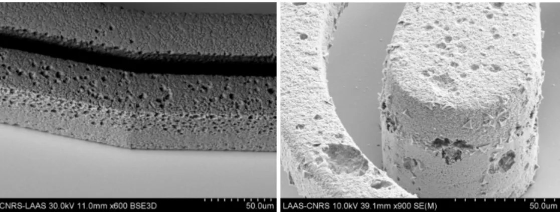
Figure 4: Positive and negative copper structures 10 µm wide and 90µm high obtained using BPN resist. These structures were characterized using HITACHI S-3700N scan electron microscope.
The BPN dissolution process appears to be very simple. It can easily be achieved and does not require heavy investments (as a plasma reactor would).One gets a complete, fast dissolution with no damage to surrounding materials. This result cannot be achieved with SU-8.
5. THE DEVICE
a b Figure 5: Integrated L+C filter(a), High quality factor inductances (b)
Among other things, the BPN resist has led to the creation of an integrated L+C filter for DC-DC applications [13] and high quality factor inductances [14]. The fabrication of these devices could not have been contemplated with the SU-8
Proc. of SPIE Vol. 7972 79722F-7
for many reasons. Firstly, because an SU-8 layer is already used as dielectric under the inductances and as the latter are made of copper no stripping solution could be envisaged.
6. CONCLUSION
In this article, a process has been described for the use of a new negative resist, BPN, which in many respects, constitutes a very good alternative to the SU-8 resist film.
First, it is easy to fabricate by utilizing standard microelectronics equipment. It can be used quickly: it is six times quicker to fabricate. It yields aspect ratios that are equivalent to those obtained with SU-8 which is used as reference. It also features very low stress values, by a factor of 10 relative to the SU-8. And last but not least, it can be removed very quickly without damaging the surrounding materials.
This new resist will support the development of new processes in the field of electrochemistry applied to microsystems. It has been validated for use as a mold in electrochemical depositions. But it also offers a great potential in other domains such as Deep Reactive Ion Etching (DRIE), packaging, etc, …
This resist also presents a development potential: indeed, one can still optimize the parameters of use to increase the aspect ratio for regular thicknesses and also to develop much higher thicknesses.
This is the first study devoted to the use of the BPN resist and we are still in the early stages of its development. Its main features already support the view that it could be a very good candidate to replace SU-8 resists in the field of electrochemistry.
ACKNOWLEDGMENTS
The authors acknowledge the support of RENATECH (the French Network of Major Technology Centres) within LAAS-CNRS, Toulouse, France.
REFERENCES
[1] http://www.microchem.com/resources/tok ebeam resist.pdf
[2] Fabrication of thick electroforming micro mould using a KMPR negative tone photoresist C H Lee and K Jiang [3] Thick photoresists for electroforming metallic microcomponents X Wei1, C-H Lee1, Z Jiang2, K Jiang1
[4] Improved registration technique for fabricating thick film A.J.M. Frood*, S.P. Beeby, M.J. Tudor, N.M. White [5] http://www.microresist.de/produkte/dupont/pdf/wbr2000series.pdf
[6] http://www.dow.com/products/product_detail.page?display-mode=tds&product=1121227
[7] Removal of SU-8 photoresist for thick film applications Paul M. Dentinger*, W. Miles Clift, Steven H. Goods [8] Wet releasing and stripping SU-8 structures with a nanoscale sacrificial layer Peihong Wanga,b, Katsuhiko
Tanaka c, Susumu Sugiyama d, Xuhan Dai a, Xiaolin Zhao a,*
[9] A comparative study of different thick photoresists for MEMS applications E. KOUKHARENKO1, M. KRAFT1, G. J. ENSELL1, N. HOLLINSHEAD2
[10] Optimized piranha etching process for SU-8 -based MEMS and MOEMS construction Matthew Holmes1, Jared Keeley1, Katherine Hurd1, Holger Schmidt2 and Aaron Hawkins1
[11] Ultrathick SU-8 mold formation and removal, and its application to the fabrication of LIGA-like micromotors with embedded roots Chien-Hung Hoa,*, Kan-Ping China, Chii-Rong Yangb, Hsien-Ming Wuc, Soon-Lin Chenc
[12] http://www.r3t.de/html/doc/MiNaT_UFER.pdf
[13] Integrated LC filter on silicon for DC-DC converter applications P. Artillan, M. Brunet, D. Bourrier, J.P. Laur, N. Mauran, L. Bary, M. Dilhan, B. Estibals, C. Alonso, J.L. Sanchez,
[14] High-Q SU-8 Based Above-IC Inductors for RF Power Devices Ayad Ghannam 1, David Bourrier 1, Christophe Viallon 1,2, Jean-Marie Boulay 3, Gerard Bouisse 3,Thierry Parra 1,2
Proc. of SPIE Vol. 7972 79722F-8