HAL Id: hal-01234061
https://hal.archives-ouvertes.fr/hal-01234061
Submitted on 26 Nov 2015
HAL is a multi-disciplinary open access
archive for the deposit and dissemination of
sci-entific research documents, whether they are
pub-lished or not. The documents may come from
teaching and research institutions in France or
abroad, or from public or private research centers.
L’archive ouverte pluridisciplinaire HAL, est
destinée au dépôt et à la diffusion de documents
scientifiques de niveau recherche, publiés ou non,
émanant des établissements d’enseignement et de
recherche français ou étrangers, des laboratoires
publics ou privés.
Ka-band low noise amplifiers based on InAlN/GaN
technologies
Séraphin Dieudonné Nsele, Charles Robin, Jean-Guy Tartarin, Laurent
Escotte, S Piotrowicz, O Jardel, S Delage
To cite this version:
Séraphin Dieudonné Nsele, Charles Robin, Jean-Guy Tartarin, Laurent Escotte, S Piotrowicz, et al..
Ka-band low noise amplifiers based on InAlN/GaN technologies. International Conference on Noise
and Fluctuations, Jun 2015, X’IAN, China. 4p., �10.1109/ICNF.2015.7288577�. �hal-01234061�
Ka-Band Low Noise Amplifiers
based on InAlN/GaN Technologies
S.D. Nsele, C. Robin, J.G. Tartarin, L. Escotte
LAAS-CNRS and University of Toulouse (UPS) F-31031, Toulouse, France
S. Piotrowicz, O. Jardel, S. Delage
III-V Laboratory 91460, Marcoussis, France
Abstract— Low noise amplifiers in receivers are usually
addressed by III-V (narrow bandgap) technologies: but when the receivers are subject to EM exposure or jamming, the need for protection devices before the active low noise amplifier (LNA) degrades the overall noise figure, and decreases the effective radio link budget. This vulnerability of the LNA can be overcome thanks to robust designs or robust technologies. Nitride technologies are investigated for power modules in transmitters and stand as promising solutions to avoid the use of limiters for robust low noise circuits in receivers. This work focuses on HF noise in InAlN/GaN HEMT devices and circuits for Ka-band SATCOM applications. Different versions of LNA have been designed at 30 GHz, in hybrid and MMIC technologies. For these designs, 1-stage and 3-stages LNAs have been realized; 1-stage amplifiers are designed to assess and study the stress tolerance under RF signal, whereas 3-stages LNAs are designed as demonstrators of operational module for receiver’s blocks (Gain>20dB featuring the lowest noise figure achievable).
Keywords—High Frequency Noise, Ka band, InAlN/GaN HEMT, LNA.
I. INTRODUCTION
If AlGaN/GaN heterostructure are now being under development (in spite of reliability studies that are still going on to push the limits of temperature-power-lifetime budgets), new solutions using InAlN/GaN are in the study phase: these HEMT devices take benefit of theoretically better interface between materials (using In content of 18% to be lattice matched on the GaN material), a better breakdown voltage and a better current density in the 2DEG. Different InAlN/GaN technological development have been studied considering their frequency and noise parameters for low noise amplifier design in Ka-band. Then different versions of hybrid and MMIC LNAs have been designed. A single stage LNA has been developed for RF stress tests, whereas a 3-stages LNA has been designed for optimized performances (Noise Figure and Gain). MMIC LNAs have also been designed. In the first section, the technology and dynamic performance of the transistor are presented for the optimized technology. HF noise parameters are proposed in the second paragraph, with also the evolution of the HF noise figure under variable signal pump conditions. Then the design and the performances of the hybrid LNA are discussed in paragraph three. Simulations of
MMIC LNA are also presented and compared to hybrid versions and to the state of the art in Ka-band.
II. INALN/GANMOS-HEMTTECHNOLOGY
The process of InAlN/GaN HEMT and MOS-HEMT devices are developed on SiC substrate by MOCVD technique (3 inches wafer); devices are optimized considering the transition frequency Ft and maximum oscillation frequency
Fmax, the output power and the low noise performances for
Ka-band applications. More details on the technology can be found in [1]. Ft=40 GHz and Fmax=110 GHz have been achieved for
the MOS-HEMT used in this study. Power densities of 3.5W/mm and power added efficiencies of 40% have been measured on 0.15µm gate length devices (6x50µm gate width) at 30 GHz for power amplifier design to target performances of 38 dBm with 18 dB of minimum gain in Ka-band over more than 20% frequency bandwidth. The optimum low noise conditions have been found for a 0.15µm gate length device featuring 2x75 µm gate width, biased at VDS=6V and
IDS=20mA. State of the art results have been published on
InAn/AlN/GaN transistors [2], featuring noise figures close to 1 dB at 26 GHz [6] or at 36 GHz [5] due to their low LG=50
nm technology: power density at 2.6 W/mm for 40% PAE is also achieved at 30 GHz by Saunier et al.
Small-signal model of the transistors have been developed, and the low-noise amplifiers designs in hybrid and MMIC have been studied both using the models and the measurements to assess the impact of the yield on the devices on the final design (more than 20 devices under test for the design of the hybrid amplifiers). The sensitivity of the model on the design procedure is accounted for and topologies can be optimized more securely.
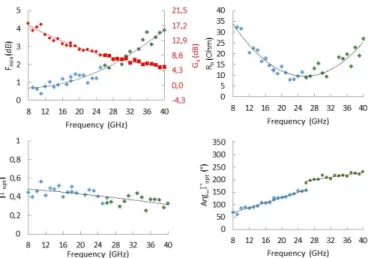
III. HF NOISE CHARACTERIZATION OF ALINN/GANHEMT Intensive HF characterization is achieved for determining the optimum sizing and biasing of the devices. First order characterization consists in measuring F50 noise figure, and
then the four noise parameters are evaluated to get accurate appreciation of the noise behavior of investigated devices (minimum noise figure of merit Fmin, equivalent noise
resistance Rn and complex optimum coefficient Γopt). A plot of
these parameters is given in figure 1 between 8 GHz and 40 GHz. It can be noticed the good concordance between the two
sub-bands (before and after 25 GHz). Only the phase of Γopt
features a small discontinuity (almost 20°), due to the change in the position of the probes on the contact pads.
Fig. 1. Noise parameters Fmin, Rn and Γopt (magnitude and argument) and
associated gain Ga versus frequency (8-40 GHz). The selected device
MOS-HEMT device (feat. 21% In content, LG=0.15µm, 2x75µm gate width,
VDS=6V and IDS=20mA) is next used during the design of the hybrid and
MMIC LNAs.
The device presents a minimum noise figure of Fmin=2 dB
at 30 GHz, with an associated gain of 7.5 dB. Moreover, as the proposed LNAs are supposed to be functional during severe jamming, the integrity of the device must be assessed under high input powers from high EM exposure (as a foreign aggression), but the low-noise characteristics should also be maintained for keeping operational the robust communication system. The nonlinear noise figure is presented in figure 2 to evidence the impact of an RF pump signal on the F50
degradation of the device (thus of the matched amplifier): for practical reasons, the RF pump frequency is set at FRF=10
GHz, and the measurement of F50 is performed at 7.5 GHz,
(which is obviously not within the frequency band under concern for the LNA). From the Pout versus Pin plot, the
compression point at 1 dB is evaluated at 2.5 dBm at the input of the device (@ 10 GHz). The noise figure F50 is measured
(at 7.5 GHz) versus the pump signal power level PRF ranging
from -30 dBm to +14 dBm.
Fig. 2. Noise figure F50 and gain of InAlN/GaN MOS-HEMT
(0.15x2x75µm²) under variable RF pump signal below and above the input 1-dB compression point (RF signal @ FRF=10 GHz, Fmeasurement=7.5 GHz) and
for a biasing at VDS=6V and VGS=-1.5V (IDS=20mA).
The noise figure F50 evolves when the input RF signal level
increases, even below the input compression point. This increase is correlated with the decrease of the gain of the transistor, but occurs before the P1dB compression point: this
non-linear behavior is attributed to the noise contribution to the effective power at the input of the device, as the noise spectral density mixes with the RF pump signal. This study allows to accurately determine the convenient sizing and biasing of the devices, in order to avoid any saturation risk under jamming signals applied at the input of the LNA.
IV. KA-BAND LOW-NOISE AMPLIFIERS DESIGN
Two technologies are investigated for the design of the LNAs at 30 GHz for SATCOM applications. Hybrid (MIC) realizations are designed using alumina and flip-chipped transistors, whereas Microwave Monolithic Integrated Circuits (MMIC) are based on GH-25 design-kit developed by UMS (United Monolithic Semiconductors).
A. Hybrid LNAs
The first designs are developed using alumina substrate and flip-chip reports of the HEMT devices. The flip-chip report is convenient to reduce the length and associated losses, as well as the inductive contribution of the wire bonding, especially at 30 GHz. Moreover, the connection by bumps can act as thermal bridges to dissipate the heat out of the active zone of the transistor. The small wavelength at 30 GHz makes possible the use of distributed matching and design techniques, whereas lumped elements are not available at this frequency. Unfortunately, instabilities may occur at 15 GHz and 7.4 GHz (for an operating frequency at 30 GHz, which is modulo two or four that of the frequencies to stabilize): distributed solutions to stabilize the circuit at these frequencies are forbidden, and a solution has been developed with MIM grounded capacitors and short lines to reduce the gain at these frequencies and get unconditionally stable amplifiers. For the 3-stages LNA, biasing circuits also contribute to the input, output and inter-stage matching networks. The inter-stage networks are also designed to optimize the noise figure, but no degree of freedom can be achieved from the serial feedback inductance brought by the flip-chip report solution (with LS=60pH): no optimization can be realized on the noise
optimal reflection coefficient which still remains close to the instabilities zones. Figure 3 is a photograph of the 1-stage hybrid Ka-band LNA. Noise figure have been measured over 4 different low-noise amplifiers, with NF measurements between 3.3 dB and 3.9 dB at 30 GHz, which is 0.3 dB above the simulated value. A photograph of the 3-stages MIC LNA is depicted in figure 4. Unfortunately, an oscillation at 7.9 GHz cannot be overcome on the 5 LNAs under test: from retro-simulation analysis, a high-pass filter must be placed at a specific part of the circuit to remove this instability, but no implementation is possible due to the small size of the estimated zone. However, the quite good agreement between simulated and measured NF on the 1-stage LNA is promising for forecasting that the 3-stage version should demonstrate NF close to simulations (NF=2.9dB at 30 GHz, and NF<3.3dB between 28.5 GHz and 30.5 GHz)
Fig. 3. Photograph of the MIC Ka-band Low-Noise Amplifier (1-stage version, flip-chipped mounted InAlN/GaN MOS-HEMT is biased at VDS=6V
and IDS=20mA). Size of the circuit is 9x7.5 mm².
Fig. 4. Photograph of the MIC Ka-band Low-Noise Amplifier (3-stages version, flip-chipped mounted InAlN/GaN MOS-HEMT are biased at VDS=6V
and IDS=20mA). Topology is different from 1-stage LNA version to optimize
NF and gain of the amplifier. Size of the circuit is 22x7.5 mm².
B. MMIC LNAs
Monolithic circuits have also been designed still based on the electrical and HF noise model of the InAlN/GaN MOS-HEMT device (same biasing conditions), with the GH-25 design kit developed by UMS. Different versions have been designed, with lumped matching networks and with distributed lines. The electrical model of the transistor is tailored to fit to the pattern of the MMIC design by de-embedding the tapers, lines and RF pads from the measured/modelled chip. The circuits have not been realized at this time, and only simulations are presented: however during the design steps, sensitivity and yield analysis have been considered to avoid the problems previously evidenced on hybrid amplifiers. Figure 5 represents the layout of a 3-stage MMIC LNA which makes use of L-C networks for matching the different input-output of the transistors (version #A).
Fig. 5. Layout of the MMIC Ka-band Low-Noise Amplifier (3-stages version #A mainly using L-C matching networks; InAlN/GaN MOS-HEMT are biased at VDS=6V and IDS=20mA). Size of the chip is 2.6x0.8mm².
Another 3-stage MMIC LNA (version #B) is presented in figure 6, based on the use of distributed lines. The coupling limit is set at -30dB between lines and pads of the layout.
Fig. 6. Layout of the MMIC Ka-band Low-Noise Amplifier (3-stages version #B with distributed matching networks; InAlN/GaN MOS-HEMT are biased at VDS=6V and IDS=20mA). Size of the chip is 3.5x1mm².
For the MMIC LNA circuits design, much more flexibility is allowed in comparison with hybrid circuits (adjustment of serial feedback, possibility to mix lumped elements and lines). For this reason, very competitive noise figure are achieved: version #A and version #B feature noise figure of 3 dB and 2.6 dB respectively at 30 GHz. The simulated performances over 26-34 GHz bandwidth show a minimum small signal gain of 20 dB, and a noise figure lower than 3.5 dB for version #B MMIC LNA. The lower quality factor of inductance (version#A) in comparison with microstrip lines (version #B) results in a larger bandwidth (+50%), and in a higher noise figure (+0.4 dB) for the same small signal gain (above 20dB for each considered bandwidth).
C. MIC and MMIC Noise Figures: this work and literature
Noise figure of LNA circuits simulated and measured are reported in figure 7. The minimum gain is 20 dB, for a frequency bandwidth set at a reflection coefficient magnitude lower than -10 dB. From the comparison between the measured and simulated 1-stage MIC low-noise amplifier, a small degradation is noticed on NF (+0.3 dB). It is expected that measurements on 3-stages versions of the LNAs would also present a good concordance between simulations and measurements. 0 1 2 3 4 5 25 27 29 31 33 35 NF (d B) Frequency (GHz) NF (d B) Frequency (GHz) NF (d B) Frequency (GHz) Simulated Hybrid 3-stages LNA
Measured & simulated
Hybrid 1-stage LNA
Simulated MMIC 3-stages LNA version #B Simulated MMIC
3-stages LNA version #A
Fig. 7. Noise figure versus frequency for different design of Hybrid and MMIC LNA based on InAlN/GaN MOS-HEMT technologies (this work). Dashed lines are for the simulations of hybrid-MIC (1- and 3-stages) and MMIC (3-stages, versions #A and #B), and solid line is for the measurement of 1-stage LNA.
Some designed LNA are reported in figure 8, with other reported results from literature based of GaN technologies [3]-[13]. Few LNAs have been designed in Ka-band, and this work presents state of the art figure of merit with NF measured at 3.3 dB (MIC LNA) or simulated at 2.6 dB or 3 dB (two versions of MMIC LNAs) at 30 GHz, in spite of a technology not yet mature.
0 1 2 3 4 5 0 5 10 15 20 25 30 35 NF (dB) Frequency (GHz) [8] [9] [10] [11] [3] [12] Simulated Hybrid 3-stages LNA (----)
Measured hybrid 1-stage LNA
(line)
Simulated MMIC 3-stages LNA version #B (….) [5] [6] [7] [13] [4]
Fig. 8. State-of-the art in GaN LNA technologies, references are largely inspired by [3]. Simulation of hybrid-MIC (dots) and MMIC version #B (dashed lines) 3-stages LNA, and measurement of 1-stage LNA (solid line) are plotted between 28 GHz and 31-32.5 GHz.
Survivability tests have been realized at 30 GHz, but are not presented in this paper: the single-stage hybrid LNA has been exposed to RF step stresses (with RF power levels higher than 20 dBm) with no destruction of the circuit. Self-biasing and non-linear effects have been noticed under elevated RF power. As the technology is not yet mature, charges are activated under high RF power and change the intrinsic operating conditions of the active device. Charges can remove after a long recovery period (up to few minutes). The technology is still under development to improve these trapping-detrapping processes.
V. CONCLUSION
The InAlN/GaN MOS-HEMT technology has been studied for the development of Low-Noise Amplifiers in Ka-band for robust receivers dedicated to SATCOM applications. The HF linear and non-linear Noise Figures have been presented for the optimum sizing and biasing conditions. State of the art Noise Figures are achieved for a single stage MIC LNA (NF=3.3dB @ 30GHz), as well as for MMIC 3-stage LNA (NF<3 dB over more than 14% bandwidth). These new wide bandgap technologies are suitable to remove the limiter usually placed before the LNA in conventional architectures, even if this technology still have to be improved to satisfy the survivability tests under elevated RF power (step stress or CW stress).
ACKNOWLEDGMENT
This work was supported by the Genghis Khan Project in the Framework of the French Research National Agency. The authors also acknowledge all the other partners of the project (Thales Communication, EGIDE, United Monolithic Semiconductors and Institut Lavoisier) for fruitful exchanges and discussion.
REFERENCES
[1] S.Piotrowicz, O.Jardel, E.Chartier, R.Aubry, L. Baczkowski, M.Casbon, C.Dua, L.Escotte, P.Gamarra, J.C.Jacquet, N.Michel, S.D.Nsele, M.Oualli, O.Patard, C. Potier, M.A.Di-Forte Poisson, S.L.Delage. “12W/mm with 0.15µm InAlN/GaN HEMTs on SiC Technology for K and Ka-Bands Applications”, IEEE IMS 2014 Conference, Tampa, USA [2] P. Saunier, M. L. Schuette, T.-M. Chou, H.-Q. Tserng, A. Ketterson, E. Beam, M. Pilla, X. Gao, “InAlN barrier scaled devices for very high fT and low-voltage RF applications,” IEEE Trans. Electron Devices, vol. 60, no. 10, pp. 3099-3104, 2013.
[3] M. Rudolph, N. Chaturvedi, K. Hirche, J. Würfl, W. Heinrich, G. Tränkle, "Highly rugged 30 GHz GaN low-noise amplifiers," IEEE Microwave and Wireless Components Lett., vol. 19, no. 4, pp. 251-253, 2009.
[4] E.M. Suijker, J.A. Hoogland, M. Van Heijningen, M. Seelman-Eggebert, R. Quay, P. Bruckner, F.E. Van Vliet, "Robust AlGaN/GaN Low Noise Amplifier MMICs for C-, Ku- and Ka-band space applications," IEEE Compound Semiconductor Integrated Circuit Symposium, 2009. CISC 2009. 4p.
[5] M. Micovic, A. Kurdoghlian, H.P. Moyer, P. Hashimoto, A. Smitz, I. Milosavljevic, P.J. Willadsen, W.S. Wong, J. Duvall, M. Hu, M. Wetzel, D.H. Chow, "GaN MMIC technology for microwave and millimeter-wave applications" in Proc. IEEE Compound Semiconductor Int. Circuits Symp. CSIC, 2005, pp. 173-176.
[6] M. Rudolph, R. Behtash, K. Hirche, J. Wurfl, W. Heinrich, G. Trankle, “A high survivable 3-7 GHz GaN Low-Noise Amplifiers,” IEEE MTT-S Int. Dig., 2006, pp. 1899-1902.
[7] H. Xu, C. Sanabria, A. Chini, S. Keller, U.K. Mishra, R.A. York, “A C-band high-dynamic range GaN HEMT low-noise amplifier,” IEEE Microwave Wireless Component Letters, Vol. 14, no.6, pp.262-264, June 2004.
[8] M.V. Aust, A.K Sharma, Y.C Chen, M. Wojtowicz, “Wide-band dual-gate GaN HEMT low noise amplifier front-end receiver electronics,” in Proc. IEEE Compound Semiconductor Int. Circuits Symp. CSIC, 2006, pp. 89-92.
[9] J.C. De Jaeger, S.L. Delage, G. Dambrine, M.A. Di Forte Poisson, V. Hoel, S. Lepilliet, B. Grimbert, E. Morvan, Y. Mancuso, G. Gauthier, A. Lefrançois, Y. Cordier, “Noise assessment of AlGaN/GaN HEMTs on Si or SiC substrates: application to X-band low noise amplifiers,” in Proc. European Gallium Arsenide Other Semiconductors Appl. Symp. 2005, pp. 229-232.
[10] D. Krausse, R. Quay, R. Kiefer, A. Tessman, H. Massler, A. Leuther, T. Merkle, S. Muller, C. Schworer, M. Mikulla, M. Schlechtweg, G. Weiman, “Robust GaN HEMT low-noise amplifier MMICs for X-band applications,” in Proc. European Gallium Arsenide Other Semiconductors Appl. Symp. 2004, pp. 71-74.
[11] R.S. Schwindt, V. Kumar, O. Aktas, J.W. Lee, I. Adesida, “Temperature-dependence of a GaN-based HEMT monolithic X-band low-noise amplifier, ” in Proc. IEEE Compound Semiconductor Int. Circuits Symp. CSIC, 2004, pp. 201-204.
[12] G.A. Ellis, J.S. Moon, D. Wong, M. Micovic, A. Kurdoghlian, P. Hashimoto, M. Hu, “Wideband AlGaN/GaN HEMT MMIC low noise amplifier, ” in IEEE MTT-S Int. Digest, 2004, pp.153-156.
[13] S. Colangeli, A. Bentini, W. Ciccognani, E. Limiti, A. Nanni, "GaN-based robust Low-Noise Amplifiers" IEEE Trans. On Electron Devices, Vol.60, no.10, October 2013, pp. 3238-3247.

![Fig. 8. State-of-the art in GaN LNA technologies, references are largely inspired by [3]](https://thumb-eu.123doks.com/thumbv2/123doknet/14421524.513433/5.892.66.423.207.419/fig-state-gan-lna-technologies-references-largely-inspired.webp)
