HAL Id: hal-01407853
https://hal.archives-ouvertes.fr/hal-01407853
Submitted on 20 Jan 2017
HAL is a multi-disciplinary open access
archive for the deposit and dissemination of sci-entific research documents, whether they are pub-lished or not. The documents may come from teaching and research institutions in France or abroad, or from public or private research centers.
L’archive ouverte pluridisciplinaire HAL, est destinée au dépôt et à la diffusion de documents scientifiques de niveau recherche, publiés ou non, émanant des établissements d’enseignement et de recherche français ou étrangers, des laboratoires publics ou privés.
Distributed under a Creative Commons Attribution - ShareAlike| 4.0 International License
Multilayer Langmuir-Blodgett films as diffractive
external 3D photonic crystal in blue OLEDs.
Frédéric Dumur, Stéphane Reculusa, Michal Mruczkiewicz, Mathias Perrin,
Laurence Vignau, Sophie Fasquel
To cite this version:
Frédéric Dumur, Stéphane Reculusa, Michal Mruczkiewicz, Mathias Perrin, Laurence Vignau, et al.. Multilayer Langmuir-Blodgett films as diffractive external 3D photonic crystal in blue OLEDs.. Optics Express, Optical Society of America - OSA Publishing, 2016, 24 (24), pp.27184-27198. �10.1364/OE.24.027184�. �hal-01407853�
Multilayer Langmuir-Blodgett films as
diffractive external 3D photonic crystal in blue
OLEDs
F
RÉDÉRICD
UMUR,
1,2S
TÉPHANER
ECULUSA,
3M
ICHALM
RUCZKIEWICZ,
4,5M
ATHIASP
ERRIN,
4L
AURENCEV
IGNAU,
5ANDS
OPHIEF
ASQUEL5,*1Aix-Marseille Université, CNRS, Institut de Chimie Radicalaire ICR, UMR 7273, F-13397 Marseille,
France
2Univ. Bordeaux, IMS, CNRS UMR 5218, F-33400 Talence, France
3Univ. Bordeaux, CNRS, Bordeaux INP, ISM-NSysA, UMR5255, ENSCBP, F-33607 Pessac, France 4Laboratoire Ondes et Matière d'Aquitaine LOMA, Université Bordeaux, CNRS, UMR 5798, 33405
Talence, France
5Bordeaux INP, IMS, CNRS UMR 5218, F-33400 Talence, France
Abstract: Three-dimensional Langmuir-Blodgett films made of silica beads are theoretically
and experimentally investigated in order to improve the relatively small efficiency of blue OLEDs. Using films made of 5 layers of beads, we fabricated OLEDs emitting at 476 nm, and measured a gain of around 40% on their external quantum efficiency. An optical model has been developed to accurately handle the fact that the organic emitting layer and the photonic extraction layer are separated by a distance greater than 1000 wavelength. The latter also permits to describe rapidly this three-dimensional optical OLED cavity, without redoing all the numerical simulations when the optical properties of the organic layers are changed (material index, thicknesses).
OCIS codes: (230.0250) Optoelectronics; (230.5298) Photonic crystals; (250.3680) Light-emitting polymers.
References and links
1. C. W. Tang and S. A. Van Slyke, “Organic electroluminescent diodes,” Appl. Phys. Lett. 51(12), 913–915 (1987).
2. X. Yang, X. Xu, and G. Zhou, “Recent advances of the emitters for high performance deep-blue organic light-emitting diodes,” J. Mater. Chem. C Mater. Opt. Electron. Devices 3(5), 913–944 (2015).
3. M. Zhu and C. Yang, “Blue fluorescent emitters: design tactics and applications in organic light-emitting diodes,” Chem. Soc. Rev. 42(12), 4963–4976 (2013).
4. J. Huang, J.-H. Su, and H. Tian, “The development of anthracene derivatives for organic light-emitting diodes,” J. Mater. Chem. 22(22), 10977–10989 (2012).
5. K. S. Yook and J. Y. Lee, “Organic materials for deep blue phosphorescent organic light-emitting diodes,” Adv. Mater. 24(24), 3169–3190 (2012).
6. L. Xiao, Z. Chen, B. Qu, J. Luo, S. Kong, Q. Gong, and J. Kido, “Recent progresses on materials for electrophosphorescent organic light-emitting devices,” Adv. Mater. 23(8), 926–952 (2011).
7. H. Benisty, H. D. Neve, and C. Weisbuch, “Impact of planar microcavity effects on light extraction-Part I: basic concepts and analytical trends,” IEEE J. Quantum Electron. 34(9), 1612–1631 (1998).
8. H. Benisty, H. D. Neve, and C. Weisbuch, “Impact of planar microcavity effects on light extraction-Part II: selected exact simulations and role of photon recycling,” IEEE J. Quantum Electron. 34(9), 1632–1643 (1998). 9. K. Meerholz and D. C. Muller, “Outsmarting waveguide losses in thin-film light-emitting diode,” Adv. Funct.
Mater. 11(4), 251–253 (2001).
10. T. Tsutsui, M. Yahiro, H. Yokogawa, K. Kawano, and M. Yoko-yama, “Doubling coupling-out efficiency in organic light-emitting devices using a thin silica aerogel layer,” Adv. Mater. 13(15), 1149–1152 (2001). 11. C. F. Madigan, M. H. Lu, and J. C. Sturm, “Improvement of output coupling efficiency of organic light-emitting
diodes by backside substrate modification,” Appl. Phys. Lett. 76(13), 1650–1652 (2000).
12. A. Chutinan, K. Ishihara, T. Asano, M. Fujita, and S. Noda, “Theoretical analysis on light-extraction efficiency of organic light-emitting diodes using FDTD and mode-expansion methods,” Org. Electron. 6(1), 3–9 (2005). 13. R. Meerheim, M. Furno, S. Hofmann, B. Lüssem, and K. Leo, “Quantification of energy loss mechanisms in
14. O. Lozan, M. Perrin, B. Ea-Kim, J. M. Rampnoux, S. Dilhaire, and P. Lalanne, “Anomalous light absorption around subwavelength apertures in metal films,” Phys. Rev. Lett. 112(19), 193903 (2014).
15. K. Saxena, V. K. Jain, and D. S. Mehta, “A review on the light extraction techniques in organic electroluminescent devices,” Opt. Mater. 32(1), 221–233 (2009).
16. X.-B. Shi, M. Qian, Z.-K. Wang, and L.-S. Liaoa, “Nano-honeycomb structured transparent electrode for enhanced light extraction from organic light-emitting diodes,” Appl. Phys. Lett. 106(22), 223301 (2015). 17. K. Ishihara, M. Fujita, I. Matsubara, T. Asano, S. Noda, H. Ohata, A. Hirasawa, H. Nakada, and N. Shimoji,
“Organic light-emitting diodes with photonic crystals on glass substrate fabricated by nanoimprint lithography,” Appl. Phys. Lett. 90(11), 111114 (2007).
18. Y. Zhang and H. Aziz, “Very high efficiency phosphorescent organic light-emitting devices by using rough indium tin oxide,” Appl. Phys. Lett. 105(1), 013305 (2014).
19. A. Kumar, R. Srivastava, P. Tyagi, M. N. Kamalasanan, and D. S. Mehta, “Outcoupling efficiency enhancement in organic light emitting diodes via nano-structured indium tin oxide and nano-phosphors,” Org. Electron. 13(12), 2879–2886 (2012).
20. A. Kumar, R. Srivastava, M. N. Kamalasanan, and D. S. Mehta, “Enhancement of light extraction efficiency of organic light emitting diodes using nanostructured indium tin oxide,” Opt. Lett. 37(4), 575–577 (2012). 21. Y. Bai, J. Feng, Y.-F. Liu, J.-F. Song, J. Simonen, Y. Jin, Q.-D. Chen, J. Zi, and H.-B. Sun, “Outcoupling of
trapped optical modes in organic light-emitting devices with one-step fabricated periodic corrugation by laser ablation,” Org. Electron. 12(11), 1927–1935 (2011).
22. R. Bathelt, D. Buchhauser, C. Garditz, R. Paetzold, and P. Wellmann, “Light extraction from OLEDs for lighting applications through light scattering,” Org. Electron. 8(4), 293–299 (2007).
23. H. Greiner, “Light extraction from organic light emitting diode substrates: simulation and experiment,” Jpn. J. Appl. Phys. 46(7A), 4125–4137 (2007).
24. T.-W. Koh, J.-A. Spechler, K. M. Lee, C. B. Arnold, and B. P. Rand, “Enhanced outcoupling in organic light-emitting diodes via a high-index contrast scattering layer,” ACS Photonics 2(9), 1366–1372 (2015).
25. Y. Sun and S. R. Forrest, “Enhanced light out-coupling of organic light-emitting devices using embedded low-index grids,” Nat. Photonics 2(8), 483–487 (2008).
26. S. Reculusa and S. Ravaine, “Synthesis of colloidal crystals of controllable thickness through the Langmuir-Blodgett technique,” Chem. Mater. 15(2), 598–605 (2003).
27. P. Massé, S. Reculusa, and S. Ravaine, “Elaboration of photonic crystal heterostructures by the Langmuir– Blodgett method,” Coll. Surf. A. 284-285, 229–233 (2006).
28. M. Parchine, J. McGrath, M. Bardosova, and M. E. Pemble, “Large area 2D and 3D colloidal photonic crystals fabricated by a roll-to-roll Langmuir–Blodgett method,” Langmuir 32(23), 5862–5869 (2016).
29. T. D. Schmidt, B. J. Scholz, C. Mayr, and W. Brütting, “Efficiency analysis of organic light-emitting diodes based on optical simulations,” IEEE JSTQE 19, 5 (2013).
30. A. A. Shcherbakov, A. V. Tishchenko, D. S. Setz, and B. C. Krummacher, “Rigorous S-matrix approach to the modeling of the optical properties of OLEDs,” Org. Elec. 12, 654–659 (2011).
31. T. D. Schmidt, L. J. Reichardt, A. F. Rausch, S. Wehrmeister, B. J. Scholz, C. Mayr, T. Wehlus, R. Mac Ciarnáin, N. Danz, T. C. G. Reusch, and W. Brütting, “Extracting the emitter orientation in organic light-emitting diodes from external quantum efficiency measurements,” Appl. Phys. Lett. 105(4), 043302 (2014). 32. P. Bienstman, P. Vandersteegen, and R. Baets, “Modeling gratings on either side of the substrate for light
extraction in light-emitting diodes,” Opt. Quantum Electron. 39(10-11), 797–804 (2007).
33. Y. Setoguchi and C. Adachi, “Suppression of roll-off characteristics of electroluminescence at high current densities in organic light emitting diodes by introducing reduced carrier injection barriers,” J. Appl. Phys. 108(6), 064516 (2010).
34. L. Zhang, H. Nakanotani, and C. Adachi, “Capacitance-voltage characteristics of a 4,4′
-bis[(N-carbazole)styryl]biphenyl based organic light-emitting diode: Implications for characteristic times and their distribution,” Appl. Phys. Lett. 103(9), 093301 (2013).
35. T. Aimono, Y. Kawamura, K. Goushi, H.-T. Yamamoto, H. Sasabe, and C. Adachi, “100% fluorescence efficiency of 4,4′4′-bis[(N-carbazole)styryl]biphenyl in a solid film and the very low amplified spontaneous emission threshold,” Appl. Phys. Lett. 86(7), 071110 (2005).
36. D. Yokoyama, “Molecular orientation in small-molecule organic light-emitting diodes,” J. Mater. Chem. 21(48), 19187–19202 (2011).
37. R. R. Chance, A. Prock, and R. Silbey, “Lifetime of an emitting molecule near a partially reflecting surface,” J. Chem. Phys. 60(7), 2744–2748 (1974).
38. R. R. Chance, A. Prock, and R. Silbey, “Molecular fluorescence and energy transfer near interfaces,” Adv. Chem. Phys. 37, 1–65 (1978).
39. J. A. E. Wasey and W. L. Barnes, “Efficiency of spontaneous emission from planar microcavities,” J. Mod. Opt. 47(4), 725–741 (2000).
40. G. W. Hanson, “Dyadic Green’s function for a multilayered planar medium – A dyadic eigenfunction approach,” IEEE Trans. On Antennas and Prop. 52 (12), December 2004.
41. V. N. Kourkoulos, A. C. Cangellaris, “Accurate approximation of green’s functions in planar stratified media in terms of a finite sum of spherical and cylindrical waves,” IEEE Trans. On Antennas and Prop. 54(5), May (2006).
42. Organic Light-Emitting Diodes (OLEDs) Materials, Devices and Applications, Alastair Buckley, ed. (Elsevier, 2013).
43. J. Yang, J.-P. Hugonin, and P. Lalanne, “near-to-far field transformations for radiative and guided waves,” ACS Photonics 3(3), 395–402 (2016).
44. M. C. Gather, M. Flämmich, N. Danz, D. Michaelis, and K. Meerholz, “Measuring the profile of the emission zone in polymeric organic light-emitting diodes,” Appl. Phys. Lett. 94(26), 263301 (2009).
45. L. Novotny and B. Hecht, Principles of Nano-Optics (Cambridge University Press 2012).
46. M. Flämmich, J. Frischeisen, D. S. Setz, D. Michaelis, B. C. Krummacher, T. D. Schmidt, W. Brütting, and N. Danz, “Oriented phosphorescent emitters boost OLED efficiency,” Org. Elec. 12(10), 1663–1668 (2011). 47. L. Peres, V. Vigneras, and S. Fasquel, “Frequential and temporal analysis of two-dimensional photonic crystals
for absorption enhancement in organic solar cells,” Sol. Energy Mater. Sol. Cells 117, 239–245 (2013). 48. S. Fan and J. D. Joannopoulos, “Analysis of guided resonances in photonic crystal slabs,” Phys. Rev. A 65,
235112 (2002).
49. K.-Y. Peng and D.-H. Wei, “Improving light extraction of organic light-emitting devices by attaching nanostructures with self-assembled photonic crystal patterns,” Int. J. Photoenergy 2014, 936049 (2014). 50. C. Fietz, Y. Urzhumov, and G. Shvets, “Complex k band diagrams of 3D metamaterial/photonic crystals,” Opt.
Express 19, 19027–19041 (2011).
51. See also the website http://www.comsol.com, and in particular the links to: http://www.comsol.com/model/download/233911/models.rf.rcs_sphere.pdf and http://www.comsol.fr/blogs/modeling-electromagnetic-waves-periodic-structures/
52. L. Peres, V. Vigneras, and S. Fasquel, “Light trapping efficiency of organic solar cells with large period photonic crystals,” Opt. Express 22(S5 Suppl 5), A1229–A1236 (2014).
53. T. H. Cormen, C. E. Leiserson, R. L. Rivest, and C. Stein, Introduction to Algorithms, Second Edition (MIT Press and McGraw-Hill 2001), pp. 540–549.
54. B. Ruhstaller, E. Knapp, B. Perucco, N. Reinke, D. Rezzonico, and F. Mueller, Advanced Numerical Simulation
of Organic Light-Emitting Devices, Optoelectronic Devices and Properties, O. Sergiyenko, ed. (InTech 2011).
55. E. Knapp, R. Häusermann, H. U. Schwarzenbach, and B. Ruhstaller, “Numerical simulation of charge transport in disordered organic semiconductor devices,” J. Appl. Phys. 108(5), 054504 (2010).
56. N. C. Erickson and R. J. Holmes, “Investigating the role of emissive layer architecture on the exciton recombination zone in organic light-emitting devices,” Adv. Funct. Mater. 23(41), 5190–5198 (2013). 57. J. Kalinowski, L. C. Palilis, W. H. Kim, and Z. H. Kafafi, “Determination of the width of the carrier
recombination zone in organic light-emitting diodes,” J. Appl. Phys. 94(12), 7764–7767 (2003).
58. J. Yang, M. Perrin, and P. Lalanne, “Analytical formalism for the interaction of two-level quantum systems with metal nanoresonators,” Phys. Rev. X 5(2), 021008 (2015).
59. H. Riel, S. Karg, T. Beierlein, B. Ruhstaller, and W. Rieß, “Phosphorescent top-emitting organic light-emitting devices with improved light outcoupling,” Appl. Phys. Lett. 82(3), 466 (2003).
60. J.-J. Kim, J. Lee, S.-P. Yang, H. G. Kim, H.-S. Kweon, S. Yoo, and K.-H. Jeong, “Biologically inspired organic light-emitting diodes,” Nano Lett. 16(5), 2994–3000 (2016).
1. Introduction
Since the discovery of the green electroluminescence of tris(8-hydroxyquinoline)aluminum Alq3 by Tang and van Slyke in 1987 [1], a revolution in the field of photonics on basis of organic materials has been initiated, and led to the production of OLED-based displays at the industrial level. Today, one important topic concerns the fabrication of highly emissive blue OLEDs, in particular for the development of full-color displays and lightings [2–6]. These devices typically consist in a stack of organic layers sandwiched between one metallic (Aluminum) and one transparent (ITO) electrode. When a voltage is applied, holes and electrons are injected within the organic layers and recombine in a specific layer, namely the Emissive Layer (EML), turning electrical power into light. It is particularly difficult to fabricate high performance blue emitters because of their intrinsically wide bandgaps. Indeed, charge injection is hindered by the mismatch of EML energy levels with those of the adjacent layers. Besides, the produced light turns out to be strongly coupled to the optical modes of the metallo-dielectric stack waveguide, and tends to remain inside the medium of high optical index. This total internal reflection effect that occurs both in conventional planar bottom-emitting organic and inorganic light bottom-emitting devices is responsible for the low outcoupling efficiency [7–12] – Typically 20% of the electrogenerated photons are coupled to free space [13]. Most of the remaining 80% excite lossy guided modes in the organic material, as well as a complex set of surface waves at the metal / organic interface, often denoted “surface plasmon” [14], that eventually dissipates as heat. In order to increase the yield, it has been proposed to introduce a patterned structure to improve light outcoupling [15].
Patterning the inner layers of large area OLEDs for internal outcoupling is a challenge [16], and may also have incidence on the color of the final OLED [17]. Therefore, we choose to structure the outer surface of a bottom emitting OLED, for technological reasons [18–21]. In many cases, the outcoupling layers are made of microstructures such as microparticles [22], microlenses [23], micro and nano-voids assembled in a monolayer [24], or periodic structures deposited on top of the glass substrate [25]. However, some of these nanopatterned diffractive grating structures involve complex and expensive elaboration processes, far from the stringent requirements of ease of fabrication for OLEDs mass production. Some disordered extraction layers [24] are easier to fabricate, but their optical properties may be difficult to model, leading to tough engineering steps in order to optimize the yield of the device. Besides, it is unsure that their fabrication would be reproducible at large, industrial scale. The Langmuir-Blodgett (LB) technique, on the contrary, is a very attractive way of producing ultrathin films with a precise control of the thickness, pattern size and shape [26, 27]. Besides, recent results show that this technique can be scaled up, using a roll-to-roll method [28], to make films of large surface containing several layers of dielectric beads, that could be stick onto an OLED to improve its yield, and may even be compatible with flexible OLEDs. The spatial periodicity of the extraction film, and therefore, of the whole OLED, permits to model their optical properties accurately and rapidly. To do this, we have extended to three dimensions the incoherent reflection/transmission formalism which is typically used to simulate OLEDs as unidimensional [29-31] or two-dimensional [32] systems. In particular, our model decouples the influence of internal layers and external coating, and permits to evaluate rapidly the OLED efficiency for different internal architectures (e.g. different EML thicknesses or point source location), without redoing all the computations. This leads to a better understanding of the mechanisms at stake, and makes it possible to obtain quantitative predictions on the improvement of light extraction, in which the 3D optical but also the 1D electrical OLED architecture plays an important role.
In Section 2, the fabrication of the device (extraction layer and then OLED) is detailed. Section 3 deals with the numerical model. Results are discussed in section 4.
2. Experimental details of fabrication
The experimental procedure can be divided in two main steps. First, a Langmuir-Blodgett film is deposited on one side of a glass substrate, and in a second step, the OLED is fabricated by evaporation on the other side. Note that the beads are bound together and to the substrate strongly enough so that no exceptional care had to be taken when handling the device during the fabrication steps.
2.1 Synthesis of silica particles and formation of the Langmuir-Blodgett film
As described in the literature, bare or surface-modified colloids presenting an amphiphilic behavior can be spread at an air-water interface and form a Langmuir Blodgett Film (LBF), thus behaving like surfactants or other molecules with a hydrophilic-hydrophobic balance. After compression with a mobile barrier, a compact monolayer of particles can then be obtained and transferred on a large variety of substrates, provided these ones are hydrophilic. In this work, we have used silica particles that were prepared following classical Stöber recipes [26]. Whereas 300 nm beads were synthesized in one single step, 600 nm beads were obtained after a growth-seeded process to get the targeted final size. In a second stage, the bare silica particles were surface-modified using a large excess of aminopropyltriethoxysilane, making them dispersible in the chloroform-ethanol mixture used for the spreading. Langmuir-Blodgett experiments were carried out on a NIMA trough with a maximum working area of 1.2 cm2 and the particles were compressed until a surface pressure
of 8 mN m-1. Then, small glass pieces (1 cm2) coated with ITO on one single side were cleaned cautiously with ethanol and chloroform in an ultrasonic bath during a few minutes. After drying, two slides were put together with their ITO sides facing each other and attached
to the dipping system. This allowed the transfer of the Langmuir film only onto the non-ITO-coated sides, the latter being carried out with a fast immersion and a slow upstroke (1 mm min-1) through the air-water interface. Under these conditions, deposition of one single monolayer at each cycle can be achieved and by repeating the process several times, it is possible to get LBF with a very precise number of particle layers (up to 5, in this work), and a homogeneous thickness over a large scale. Figure 1(a) and Fig. 1(b, c) show SEM views at different scales of the LBF deposited on glass. Figure 1(d) displays a picture of the final iridescent devices.
Fig. 1. Sample SEM pictures of the Langmuir Blodgett pentalayer (a,c) and monolayer (b) of 300 nm diameter silica spheres. Picture (d) shows the final devices, each containing four OLEDs. The colour variations of the different samples are due to an iridescence effect that depends on the surface orientation.
2.2 OLED fabrication
After LBF deposition on one side of the glass substrate, OLEDs where fabricated on the other (uncoated) side. All materials (including the light emitting material BSB4, also named BSB-Cz in some studies [33–36]) used for the device fabrication were purchased from Lumtec with the best purity available and used as received. OLEDs were fabricated onto cleaned indium tin oxide (ITO) coated glass substrates with sheet resistance of 10-12 Ω/sq. Prior to organic layer deposition, the ITO substrates were successively washed with acetone, ethanol and isopropanol in an ultrasonic bath for 10 min before surface treatment with UV-ozone plasma for 20 min. This treatment had no effect on the LBF deposited on the other side of the substrate. Organic layers were then sequentially deposited onto the ITO substrate at a rate of 2–4 Å/s under secondary vacuum. Aluminum cathode was deposited through a shadow mask by thermal evaporation. Device structure is the following: ITO was used as the transparent anode / MoO3 (10 nm) as the hole injection material/ MoO3:
4,4'-bis(4-(9H-carbazol-9-yl)styryl)biphenyl (BSB4) (20 wt%, 10 nm) as the hole-transport layer, BSB4 (130 nm) as the
emission layer(EML)/2,9-dimethyl-4,7-diphenyl-1,10-henanthroline (BCP) (20 nm) as the hole-blocking layer/ tris(8-hydroxyquinolinato)aluminium (Alq3) (40 nm) as the electron
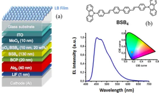
transporting material/ LiF (1 nm) as the electron injecting material and Al (80 nm) as the cathode. The Electroluminescence (EL) spectra, CIE (Commission Internationale de l’Eclairage) coordinates, current-voltage and brightness-voltage characteristics of the devices were recorded with an EQE Measurement System (model C9920-12) of Hamamatsu Photonics K.K. The device architecture, the chemical structures of the materials that were used in this work, as well as the EL spectrum and the color of the OLED are presented in Fig. 2.
Fig. 2. a) Scheme of the fabricated device. b) Formula of the fluorescent material, BSB4, EL
spectrum and color of the active material.
3. Optical modeling
Flat OLEDs, without extraction layer, can be modeled in a simple and accurate way, as a uni-dimensional multilayered waveguide coupled to an electric dipole, that mimics one emitting molecule [37–39]. The knowledge of the Green function of such multilayered media [41, 42] permits to compute rapidly some essential physical quantities such as the far field radiation diagram, the EQE, and the amount of energy coupled to the lossy guided modes [31,32], including surface plasmons [14].
However, it is much more difficult to build a model that also takes accurately into account the three-dimensional external PC layer above the thick glass substrate. In particular, it is clearly impossible to model the whole device (OLED + LBF) with direct numerical methods such as Finite Elements (FEM) or Finite Difference in Time Domain (FDTD), as the computation domain would be much too large (the substrate between organic layers and LBF is more than 1000 wavelength thick).
To overcome this problem, one assumes that the extraction layer, placed over thick and rough glass, reflects light incoherently towards the EML. Then, the emission rate of a molecule is not modified by the presence of LBF [31, 42], and the variations of EQE are only due to a change of outcoupled power, but not of Purcell factor. Under this realistic hypothesis, one can solve the problem numerically in two main steps [43].
First, the flat OLED, without LBF, will be modeled, and its radiation diagram will be computed – see 3.1. Then, the transmission coefficients of a LBF on a glass substrate, without OLED will be computed – see 3.2. Combining these studies, one can estimate the optimal parameters of the LBF (pattern, number of layer), for a given OLED architecture. Finally, a more rigorous and quantitative description of the OLED with LBF will be presented – see 3.3.
3.1 Modeling an OLED without LBF
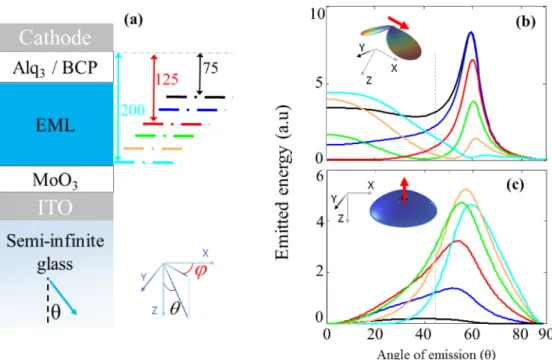
Using a numerical model developed previously [29,30], based on the theory of Chance, Prock and Silbey [37, 38], we compute the Green function of one dipole source in a multilayered planar medium, to evaluate the radiation diagram of the OLED [40, 41, 43] in a semi-infinite glass slab, see Fig. 3(a).
The OLED we study has a thick EML (130 nm) that cannot be modeled with a single dipole source, as usually done for EML as thin as 10 nm [29,30]. A distribution of dipoles should instead be considered, what leads to two main differences compared to thin EML OLEDs.
Firstly, as the exciton distribution is generally not uniform in thick EML [45], all the elementary dipoles will not emit with the same intensity. We observed experimentally that removing the hole blocking BCP layer, the charges recombine in Alq3, resulting in a green
emitting OLED. This means that in the EML, the holes’ mobility is larger than electrons’ and that the recombination zone of the OLED is asymmetric, and shifted towards the BCP / EML interface. For the sake of simplicity, we shall use a uniform probability density (constant over a width Δ) to model the exciton distribution, see section 3.3.
Secondly, each elementary emission site is located at a different distance from the metal cathode, and has therefore a different radiation diagram [45]. Figure 3 describes this effect, showing the radiation diagram of the light emitted by one dipole placed at different location inside the EML – each location corresponds to a different color. The dipole orientation also influences both the far field polarization and intensity [45, 46]. Therefore, the elementary contributions of a dipole either parallel – see Fig. 3(b) – or perpendicular – see Fig. 3(c) – to the XY stack plane have been studied. Eventually, the total energy emitted by the OLED is obtained by summing these contributions with a weight 2/3 for parallel and 1/3 for perpendicular dipole. When the dipole is parallel to the stack, the far field characteristics depend on the polar and azimuthal angles – denoted respectivelyθ and ϕ, see inset Fig. 3(a). To take into account the uncorrelated emission of randomly oriented molecules, we made averages on ϕ, so that the emitted energy, see Fig. 3(b, c), now depends only on θ. Looking at the numerical results, one notices an important variation of the angular spectrum when the dipole location changes inside the EML. As the exciton distribution is shifted towards the BCP / EML interface, the main contribution to OLED light come from the molecules located between the BCP / EML interface and the middle of EML (see the black, blue and red lines, that corresponds respectively to a distance of 75 nm, 100 nm and 125 nm from the cathode). Therefore, the emission has a maximum around θ≈60°, above the total internal reflection (TIR) angle for outcoupling to air, θTIR = arcsin (1/n) ~44° – n = 1.45 is the glass refractive
index.
Consequently, an important part of the light emitted by the exciton recombination in the OLED cannot escape to air and remains strongly coupled to the guided modes of the stack. In order to improve the performance of the device, one needs to find a way to extract the light emitted around θ ≈60° in the glass substrate.
Fig. 3. Radiation pattern of one dipole source in an OLED with thick emissive layer. Panel (a) is a scheme of the simulated device, where a semi-infinite glass medium has been considered. The detailed structure is given Fig. 2(a). An inset (bottom) shows the coordinate system, with a polar, θ, and azimuthal, ϕ, angle. For each simulation, one single point source is placed inside the EML, at different distance from the cathode (75 nm –black –, 100 nm – blue –, 125 nm – red –, 150 nm – green –, 175 nm – orange –, 200 nm – turquoise). Panel (b,c) show the energy emitted in a direction θ(see panel (a)), towards the bottom of the OLED, by a unitary dipole oriented either parallel (b) or perpendicular (c) to the XY plane of the stack. Averages on ϕhave been made in the case the dipole is parallel to the stack (panel (b)) – see text. The energy emitted at θ>θTIR ≈44° – see the vertical dashed line – can only couple to (lossy) guided modes and do not escape OLED.
3.2 Optical properties of the multilayered Langmuir-Blodgett film
It is known that guided resonances in photonic crystal slabs [47, 48] permit to couple guided modes to free space, thanks to a periodic array of dielectric or metallic inclusions. Simple models of light extraction based on this effect have been proposed [49], in which a Bragg condition permits to evaluate the minimum grating period that permits to extract light out of an OLED. However, neither the bead index and shape, nor the number of bead layers do not play any role in such model, and in the following, we shall use a more quantitative approach.
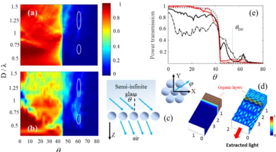
Using FEM simulation [50,51], one can compute the power transmission and reflection coefficients of the complex LBF structures that were fabricated, see Fig. 4. To do this, we considered a plane wave, TE or TM polarized, that is incident on the LBF coating, modeled using periodic boundary conditions and perfectly matched layers (PML) [50,51]. The wave direction is described by two angles, see Fig. 4(c): θ, the polar angle between incident ray and the normal to the stack planes, and φ, the azimuthal angle between one principal direction of the hexagonal lattice, and the projection of the ray on the stack plane.
Computation results are presented Fig. 4. A first example, see Fig. 4(e), shows, for ϕ=0, that some energy can be transmitted above the TIR angle, when a LBF is present, whereas it could not be transmitted without LBF. The corresponding field maps, for an angle arbitrarily chosen: θinj = 54.5°, above TIR limit, are shown in Fig. 4(d). One can clearly see that the light
transmission is associated to a resonance in the PC beads (right hand side figure), whereas no 8
light comes out if LBF is absent (left hand side figure). This is precisely the guided resonance effect [49] in a LBF, which is responsible for the outcoupling above TIR angle.
In order to investigate the LBF properties, the transmission has been computed for different bead diameters, D – that are identical to the PC period –, different angles of incidence (θ, φ) and polarizations. The results are presented Fig. 4(a, b), where the diameter is shown in units of wavelength: D/λ, and, for the sake of clarity, the transmission has been averaged on φ and on incident polarization. For both the monolayer, Fig. 4(a), and the pentalayer LBF, Fig. 4(b), one observes a high and a low transmission zone, respectively below and above TIR angle. The limit, at TIR angle, tends to fade out when the number of layer increases – compare Fig. 4(a) and Fig. 4(b). Both for a monolayer and a multilayer, transmission is possible above TIR angle, and is stronger (i) when five layers are used instead of one, (ii) when D/λ increases. Note this last observation is in agreement with the fact that the number of resonances in photonic crystal slabs increases with D/λ [52], each resonance above TIR angle being responsible for a transmission peak [48]. Note that, in the limit where D>> λ, many resonances are present so that the LBF would be described in a more appropriate way by geometrical optics, neglecting polarization effects [23].
From the results of section 3.1, one knows that the optimal LBF needs to show a high transmission around θ = 60°. It turns out that one observes several local maxima of transmission around θ = 60°, for the 5-layers LBF, see Fig. 4(b). Two of them respectively corresponds to the periods D = 300 nm and D = 600 nm. More precisely, as most of the emitted energy lies between the wavelength of 440 nm and 540 nm, see Fig. 2(b), the corresponding ratio D/ λ lie between 0.55 and 0.68 – when D = 300nm –; between 1.1 and 1.36 – when D = 600 nm. We represented these intervals by white ellipses on Fig. 4(a) and Fig. 4(b). For monolayer LBFs of the same period – see the ellipses on Fig. 4(a) –, one notice that transmission above TIR angle is much smaller. This simple analysis shows that one can expect a better extraction with five than with one layer LBFs, for the OLED we fabricated. Looking at Fig. 4(a), one does not expect a strong improvement with the monolayer LBF when D = 300 nm, whereas for D = 600 nm, a local maximum of transmission is present around θ = 60°, so that this monolayer LBF is expected to slightly improve outcoupling. Note that these trends have been confirmed by experiments (see section 4), and more detailed simulations (see section 3.3).
Finally, if one combines the information on the radiation pattern without LBF – see section 3.1 and Fig. 3 –, and the LBF transmission, one can find an optimal sphere diameter by matching the angle where emission is maximum to the angle where LBF transmission is maximum. This simple optimization criterion assumes that the outcoupling gain is due to an increase of the transmission above TIR angle, and that the transmission below TIR angle do not play an important role. This is the case, for example, if the dipole radiation diagram is narrow enough, and its peak is located above TIR angle, see e.g the red curve Fig. 3(b).
This method is rapidly scalable to other colors, as the properties of the LBF only depends on the ratio D/λ. Then, once the shape of LBF is fixed (i.e. number of layers, refraction index of the spherical inclusion), one can compute its transmission for all ( , )θ ϕ and polarization
states, and find out the optimal pattern size for any OLED architecture. Obviously, this technique can be generalized to any shape of the periodic lattice as well. However, it has some limitations.
Fig. 4. Optical properties of the multilayered Langmuir-Blodgett film. Panel (a), shows the power transmission of a monolayer LBF at wavelength λ as a function of the pattern periodD/λ, and of the θ angle, after averaging on TE-TM incident polarization and ten values of the azimuthal angle φ between 0 and 60 . Panel (b), shows the transmission for a pentalayer LBF. The modes excited by the blue emitter when D = 300 nm or D = 600 nm, and
60
θ ≈ ° are marked with an ellipse (see text). Panel (c) is a scheme of the simulated structure. Panel (d) shows the norm of electric field, in arbitrary units, with (right-hand side) and without (left-hand side) extraction layers. A plane wave is injected (from top to bottom) at λ = 476 nm, with a direction φ = 0, θinj = 54.5 > θTIR (see the dashed line panel (e)). Dimensions on field
maps in panel (d) are in microns. No light is transmitted towards the bottom half space (air) for the reference. With one LB layer (right hand figure), extraction is associated with excitation of photonic crystal resonances (hot spots) in the glass beads of 600 nm diameter. Similar results are obtained for a 5-layer photonic crystal. Panel (e) shows the power transmission for φ = 0, varying θ, for the reference (without LBF) – dotted grey –, the 300 nm period LBF (red) and 600 nm period LBF (black). Monolayers are represented in solid lines, pentalayers with dot-dashed lines.
Indeed, while LBF improves transmission above TIR angles, one notice that it gives worse results than bare glass at small θ angles, especially when the LBF contains several layers of beads – compare Fig. 4(a) and Fig. 4(b). Then, the possible gain due to guided resonances observed above TIR angle could be ruined by a transmission loss, if the dipole source also radiates at small angles. This points out a limitation of the previous method – section 3.1 and 3.2 –, where only the angle of maximum emission (here, θ = 60°) has been considered.
3.3 Modeling a three-dimensional OLED cavity with LBF
In order to overcome this limitation, we will now present a more elaborate model.
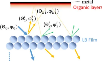
One now considers that each plane wave emitted by the molecules bounces back and forth in the organic and substrate slab, reflecting at each roundtrip on the organic / aluminum coating, and outcoupling a fraction of its energy at each refraction on the outer interface. This will permit to take all the outcoupled rays into account, and not only those that are directly transmitted through the LBF. A priori, the problem can be complex, as many rays can come out of one single scattering process (see Fig. 5).
Fig. 5. Scheme of light propagation in the multilayer with LBF. One of the plane wave emitted by some point source propagates through glass with angles (θ0 ; φ0). It reflects a first time on
the 3D photonic crystal to create several plane waves at angles (θ1i ; φ1i), which propagates
towards the organic layers (in this example two plane waves are created, and i = 1 or i = 2). This backward propagating plane wave reflects on the organic/metal multilayer and bounces upwards with an angle (θb1i, φb1i), etc…. At each roundtrip, a transmission occurs and energy
leaks out of the stack.
To implement this ray tracing method, one organizes the different contribution to extracted light in a tree structure, where every node corresponds to a scattering process. The tree is then explored using an algorithm of the “deep first search” type [53]. This permits to compute the total power as a path integral, written as in the form of a continued product:
(
)
(
)
(
)
0 0 0 0 0 0 , 0 0 1 1 1 1 2 2 ( , ) , 1 , ; ; 1 tot t b i i i t b i i j j j k P P T R R T R R T θ ϕ θ ϕ θ ϕ θ ϕ θ ϕ θ ϕ θ ϕ = + + + ……
(1)where the notation R R Tt b
(
; θ ϕ θ ϕ1i 1i 2j 2j)
represents the product of top, bottom reflectioncoefficients and transmission coefficient during the elementary path that goes from ray i of 1st scattering process to ray j of 2nd scattering process. Note that reflection and transmission coefficients also depend on the polarization state of the incident light, and not only on the direction of the incident ray. P( , )θ ϕ0 0 is the power radiated by the point source in the layered material. To accelerate this ray tracing procedure, we look for loops that occur when (θb pi, φb pi) = (θb p-1 i, φb p-1i). Indeed, their contribution can be factorized, and the continued product
then reads: 0 0 0 0 , ( , ) 1 l tot t b res l loop l l T P P P R R θ ϕ θ ϕ ∈ = + −
(2)where Rb and Rt are the reflection coefficients of the bottom and top interfaces, and T the
transmission coefficient. Pres is the residual power coming from rays which do not form
simple closed loops and is computed by summing on the successive scattering processes, until numerical convergence is reached.
A key point in the model is that P( , )θ ϕ0 0 on one hand, and the reflections and
transmission coefficients of the photonic structure on the other hand, are independent. This means that once the photonic structure has been characterized, see section 3.2, it is fast to evaluate the OLED efficiency for different situations, corresponding for example, to different point source locations, different arrangements (index, thicknesses) of the organic layers.
We have just described the excitation of a periodic layer made of a complex stack of glass spheres, by a plane wave issued from a unique point source. However, to model the OLED and compare with experimental results, we now need to consider many independent punctual sources, distributed in the zone where excitons recombine [44], see 3.1. The total extraction gain shall then be obtained by integration over different location of the thin dipole sheet inside the thick EML.
Let us focus here on the best extracting LBF, of period D = 600nm with 5 layers of beads (similar results have been found for the other LBFs). Fig. 6(a) (see the black dashed line) shows that, in the present architecture, a maximum of extraction could occur with a large enhancement (≈220%), if the source were a thin layer of dipoles located at the center of EML, see the red line Fig. 3(b). Note that similar dependency on the source location has been observed for flat OLEDs with thin EML, in the ideal case where all the energy trapped in the substrate is extracted (using a semi-spherical macroextractor, see [31].). In this later work, the thin EML (10 nm) acts as an infinitesimal sheet of dipoles, and its location was varied by changing the thickness of the ETL, whereas in our case, the EML is thick (130 nm) so as to improve the resistance of the device to high voltage. Eventually, total extraction gain shall be computed by integration on the exciton distribution [54]. These later have been studied theoretically [55,56] and experimentally [56, 57] and depends on the OLED structure, as well as hole and electron mobilities. Using a simple step distribution (constant exciton density over a width Δ), we evaluated the OLED gain, Fig. 6(b), and obtain a good agreement with experimental results, see Table 1, for some reasonable width of 60 nm of the exciton distribution.
Fig. 6. panel (a): extraction gain (dashed line) obtained when only one thin layer of dipoles emits. Dipole are randomly oriented and placed inside the EML, at different distances from the BCP/EML interface of an OLED covered with a 5-layers LBF of period D = 600 nm (see the scheme in inset). The colored background symbolizes a uniform exciton distribution, of width Δ. In panel (b) the total extraction gain is shown. It has been obtained by integration of local gain on the exciton distribution.
4. Results and discussion
To assess the outcoupling efficiency of the LBF, blue OLEDs were fabricated with a benchmark fluorescent emitter i.e. BSB4. Two types of silica beads – 300 and 600 nm of
diameter – were used, to make monolayer, bilayer and pentalayer films, organized by the Langmuir-Blodgett technique.
Reference devices without light-outcoupling layer were also fabricated to evidence the benefits of these nanostructures. OLEDs were fabricated according to the method described in the experimental section with configuration: ITO/MoO3 (10 nm)/ MoO3:BSB4 (20 wt%, 10
nm), BSB4 (130 nm)/ BCP (20 nm)/ Alq3 (40 nm)/ LiF (1 nm)/ Al (80 nm). The measured
characteristics are presented in Table 1.
Prior to investigations on a possible increase of light scattering, electrical characteristics of the pristine devices and devices with a LB Film (LBF) were examined. As evidenced by a careful control of their I-V (current/voltage) curves, OLEDs characteristics were clearly identical, guaranteeing that the modification of the EL intensity only arises from the capping layer. Device performances with and without optical outcoupling layers have been verified in three separate batches with multiple OLEDs per batch.
Table 1. Summary of EL characteristics of the fabricated OLEDs
Device Vturn-on
(V)[a] (x,y)CIE [b] (nm) λEL L
[c] (cd/m2) Current eff.[c] (cd/A) Power eff. (lm/W) [c] EQE (%)[c ] Power effx EQE x Reference device 4.2 0.163, 0.255 477 10900 (12.2 V) 2.41 0.76 1.37 1 1 Monolayer LBF (D = 300 nm) 4.3 0.166, 0.252 478 (12.2 V) 12200 2.43 0.80 1.43 1.05 1.04 Monolayer LBF (D = 600 nm) 4.1 0.162, 0.249 477 (11.8 V) 21700 2.77 0.86 1.66 1.13 1.21 Bilayer LBF (D = 600 nm) 4.2 0.161, 0.254 478 25320 (11.2) 2.81 0.99 1.70 1.22 1.24 Pentalayer LBF (D = 600 nm) 4.7 0.163, 0.250 478 (11.2 V) 30200 3.43 1.00 1.89 1.52 1.38
EQEx (resp. Power Effx) is the EQE (resp. Power efficiency) enhancement factor vs. the reference device without LBF. a) Turn-on voltage at a brightness of 1 cd/m2. b) Values measured at 100 mA/cm2. c) Maximum value.
Electroluminescent characteristics were first examined for OLEDs capped by a monolayer of silica particles with either D = 300 nm or D = 600 nm. As can be seen from Table 1, for the whole range of current density examined, the Power Efficiency (PE) as well as the EQE were sensibly enhanced upon introduction of a monolayer LBF with D = 600 nm. Enhancement factors of 1.13 (Power Effx) and 1.21 (EQEx) were measured, respectively for the PE and the
EQE. The improvement of the EL performance was much smaller for OLEDs capped with a monolayer LBF with period D = 300 nm (see Table 1) and no further investigations were carried out on LBF of 300 nm period.
In parallel to the electrical characteristics, one could wonder if the LBF also influences the spectral characteristics of the emitted light. This phenomenon has been observed for OLED with internal extractors [16, 17] and is a general feature that can arise when a resonator of any size (here the OLED stack with or without photonic crystal) is coupled to an emitter [58]. This could lead to an unwanted modification of the spectrum of emitted light [17], that could even depend on the driving current. Such phenomenon was not observed here, as the spectral shape and OLED color, see Fig. 7(b), remain unaffected by the injection rate. This indicates that no significant shift of the recombination zone with the driving voltage was present, which is a sign of a good confinement of excitons within the emissive layer.
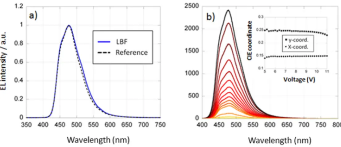
Fig. 7. a) Electroluminescence spectra of OLEDs with a LBF with spheres of 600 nm (blue solid line) and reference device (black dashed line). b) Variation of EL spectra and CIE coordinates with the applied voltage.
Simply, careful examination of the EL emission revealed that the EL spectrum of the capped OLEDs is slightly broader than the EL spectrum of the uncapped OLEDs, see Fig. 7(a). This is a known phenomenon, attributable to interference effects [59]. Note that this observation is in agreement with the hypothesis used section 3, that the EQE gain is not due to a change of Purcell factor but of light outcoupling. In the two cases we studied, the EL intensity was maximum at 476 nm with a full width at half maximum (FWHM) of 73 nm. A blue light with CIE coordinates of (0.15, 0.24) was obtained.
Then, a second series of devices was fabricated, using now a 5-layers LBF. Similarly, we observed that the EL spectrum almost does not change when the OLED is caped, but the EQE enhancement now reached a factor of 1.38 (see Table 1). This result is consistent with the aforementioned theoretical calculations (factor of 1.4). An enhancement factor of 1.32 was also determined for the power efficiency (see Table 1). At first sight, one can be surprised that the turn-on voltage is slightly higher for the 600nm pentalayer OLED than for the monolayer OLEDs. In fact, by increasing the thickness of the light outcoupling layer from one to five layers of silica spheres, one also increases its absorption – the glass beads always have some tiny losses. This additional loss channel shifts the detection threshold of 1 cd/m2 to a slightly
higher voltage.
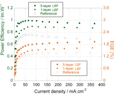
Figure 8 shows the enhancement of power efficiency and EQE for devices with one or five layer LBF and the reference device, as a function of the driving current. We also observed an improvement of the current efficiency (cd/A), the PE (lm/W). Finally, let us mention that for a given voltage, a higher luminance was measured for OLEDs with a 5-layer LBF, compared to OLEDs with a monolayer LBF and reference OLED. For exemple at 11.2V, the brightness of devices with a LBF was ca. 3-times higher than that of the pristine devices, with a luminance increasing from 10400 cd/m2 to 30200 cd/m2.
Fig. 8. Effect of the LBF on OLEDs characteristics. Reference device and OLEDs with one and five layers of 600 nm silica particles are compared. Power efficiency (PE, lm/W) and External Quantum Efficiency (EQE, %) are represented (respectively in green and orange plots) as a function of the current density.
5. Conclusion
In summary, we propose to increase the efficiency of blue OLEDs by putting a structured 3D coating elaborated by Langmuir-Blodgett technique on the outer side of the OLEDs, and we obtain a EQE gain close to 40%. Additionally, we have shown that the LBF period can be determined by a simple matching condition between the direction of light emission in the glass substrate, and the angle where LBF transmission is maximum. Then, we extended to three dimensions the well-known unidimensional model of OLED cavities, taking advantage of a decoupling between emission and extraction processes. In this way we are able to model complex photonic structures, which are optically thick, taking into account all the rays diffused by the extraction coating. The experimental results, in agreement with the numerics, show that it is important to use a multilayered film, that can be fabricated at large scale and low cost e.g. by roll to roll processes [28], but not by spin-coating techniques [49]. Perspectives could concern the design of 3D OLED such as bio-inspired architectures [60] and OLED with thick emissive layers for which a joint work on electrical and optical modeling is necessary, as the exciton distribution will have an influence on the optimal LBF period.
Funding
French National Research Agency (ANR)( ANR-10-EQPX-28-01/Equipex ELORPrintTec, and ANR-13-BS08-0003 / PhotoLighT), State of Aquitaine, SMOLED project (number 2014 - 1R6306).


![Table 1. Summary of EL characteristics of the fabricated OLEDs Device V turn-on (V) [a] CIE (x,y) [b] λ EL (nm) L [c] (cd/m 2 ) Current eff.[c] (cd/A) Power eff](https://thumb-eu.123doks.com/thumbv2/123doknet/14516002.530561/14.918.165.736.395.641/table-summary-characteristics-fabricated-oleds-device-current-power.webp)