Abstract--With the increasing demand of higher operating frequencies for electronic circuits, the printed circuit board designers face more electromagnetic radiation problems than ever. Some “rules-of-thumb” are employed to help the designers to reduce the radiation problems. The 20H rule is one of printed circuit design rules, which intends to minimize the electromagnetic radiation. This project focuses on analysis and simulation of 20H rule’s signal propagation mechanisms. The model used in the project is a 2D planar structure. The numerical electromagnetic method, Finite Difference Time Domain (FDTD) method, is used for the field computation and analysis. Simulation is based on various structures of model and different distributions of excitation sources. Analysis focuses on the signal propagation models. Field distributions and radiation patterns are visualized by mathematical software. Meanwhile, Poynting vectors are calculated to give quantitative expression. The simulation results indicate three factors, namely, operating frequency, size of PCB and separation distance that will affect the function of 20H rule. The effects of three factors are shown by comparison of specific cases in this thesis.
Index Terms-- PCB, 20H Rule, FDTD and EMI/EMC.
I. INTRODUCTION
IMULATION as a method is rapidly pervading decision-making, and training of all kinds. It is particularly important in electromagnetic area. With the advancement in electronic devices and high frequency circuits, Electromagnetic Interface and Electromagnetic Compatibility (EMI/EMC) issues have greatly increased in complexity. Some hands-on design techniques are used in order to pass the EMC test. The 20H rule, one of the printed circuit board design rules, is used to minimize the electromagnetic radiation on nearby circuit. In practice, 20H rules are implemented by extending the length of PCB ground plane by 20 times the separation distance of two PCB planes. But the effects and working mechanism are still under discussion in academia. In order to
Y. Jiang and LW Li are with High Performance Computation for Engineered Systems (HPCES) Programme, Singapore-MIT Alliance, National University of Singapore (NUS), 10 Kent Ridge Crescent, Singapore 119260. LW Li is also with Department of Electrical and Computer Engineering, NUS, 10 Kent Ridge Crescent, Singapore 119260.
EP Li is with the Institute of High Performance Computing(IHPC), 89C Science Park Drive #02-11/12, Singapore, 118261
.
The work described herein has been sponsored by the IHPC of NUS.
get more physical insights, numerical electromagnetic simulation method, namely, Finite Difference Time Domain (FDTD) method is used in this project to simulate radiation from PCB board before and after implementing the 20H rule. Results and discussions follow after simulation.
EMI/EMC research aims to obtain electromagnetic radiation performances inside electronic devices. With advent of high-frequency devices, it is almost impossible to rely exclusively on traditional techniques. As a result, application of computational electromagnetic to EMC/EMI engineering problems becomes an emerging technology.
Simulation in this project is based on numerical methods for electromagnetic. FDTD method, one of well-defined computational electromagnetic scheme, is selected because of its accuracy and relatively small needs for computation resources. 2D planar structure is used to represent our PCB structure. Efforts have also been paid to find a quantitative expression for radiation in order to investigate on emission characteristics.
With the developed simulator, detailed performance of various 20H rule implementations with different structures and different excitation sources can be analyzed. Since radiation of devices is the most important attribute in this project, we focus more on analyzing the radiation intensity and distribution. Comparisons between different lengths of devices are given for the same model.
II. BACKGROUND OF 20H RULES
Use of the 20-H rule increases the intrinsic self-resonant frequency of the PCB, because the physical dimensions of the power distribution network are altered. Since less capacitance will be present, there will be a higher self-resonant frequency of operation.
Assume that the termination value is about ten times higher than the characteristic impedance of the transmission line. In this situation, however, the "termination" is a value that will
not fully terminate the line. The position of the termination is
such that a rather long "stub," as compared to the total transmission line length, is created at the end of the line. The fringing of the flux fields depends on the exact relationship and distribution path near the plane edges. The distribution of the flux depends on the geometry of the component and its distance from the edge of the PCB.
Assume that a source located at the center of a PCB is being simulated using field solvers. Right under the circuit is a small loop area between the ground and power pins where the current between the pins is circulating. The current circulating
Design and Analysis of Printed Circuit Boards
Using FDTD Method for The 20-H Rule
Jiang Yi, Le-Wei Li and Er-Ping Li
Geometry and Material Description
Excitation
Calculation Over spatial grid in the computation Domain
Update H field Update E field
Implementations of P.E.C Boundary Condition & Perfectly Boundary
Condition
Absorbing Boundary Condition (PML)
Scientific Visualization and Calculating the Poynting Vector
in the small loop area, including the position of the bypass capacitors can be very high. These flux and fields from this component are circulating, defined by the layout shape of the device itself.
The advantage of undercutting one of the planes (e.g., usually the power plane) is that power is not wasted as dissipation at the terminations. RC terminations can be poor at specific frequencies of concern, because of the resonance of the capacitor and the inter connector traces.
III. SIMULATION MODEL AND FDTD METHOD
A. 2D Planar Structure Simulation Model
To simplify the modeling, 2-dimension model for simulating the signal propagation between the ground plane and power plane is selected.
The PCB to be modeled consists of a power plane and a ground plane as shown in Fig 1. For the 20H rule simulation, the following assumptions are made: 1. Both of ground plane and power plane are perfectly conducting and need to satisfy the PEC conditions in positions of two planes, 2. Both of two planes are infinitely thin in thickness (compared to width and length, this assumption is reasonable), 3. The simulation is based on free space. In the following discussions, H is used to denote separation distance of PCB, E denote electronic field.
Fig. 1 The 2D Planar Structure
Both ground plane and power plane are perfectly conducting plane, so PEC conditions are required to be satisfied at these two planes on which tangential electric field should be zero. The blue point inside picture stands for the excitation source in the PCB plane. Issues regarding the signal excitation such as signal type and frequency bandwidth are described in the next section.
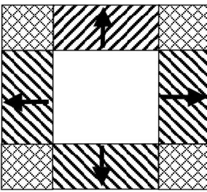
Due to limitation of computer resources, we truncated free space into finite rectangle region in which edges include reasonable perfectly match layers. After this consideration, we build our simplest simulation model.
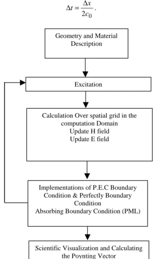
B. FDTD Method
The flow graph in Fig. 2 shows the structure of the FDTD algorithm. The first step for the FDTD simulation of a microwave structure is the geometry and material description. The dielectric interfaces and locations of the perfectly conducting surfaces are specified on the computational grid in the step. The second step is the specification of the excitation signal. Three kinds of excitation sources are considered in our simulation, they will be discussed in next section. Once the excitation signal is specified, the FDTD algorithms update all the field components on the computational grid for each step.
The updated equations are modified by the discretized forms of Maxwell’s equations. Time step satisfies stability condition, and it is simply set as
0
2c
x t= ∆
∆ .
Fig. 2 Flow Chart of FDTD Method
On the dielectric interfaces, tangential electric field components are set to zero on the grid points corresponding to perfectly conducting layers (ground plane and power plane, which have been assumed to be infinitely thin). The tangential fields components on the outer layers of the computational grids are updated by absorbing boundary condition PML.
C. Excitation Source
Two types of excitation sources are implemented in our simulation:
(1) The dipole excitation source is implemented at a single point, usually in the center of structure, by enforcing the E field at this point to a given sinusoidal function, shown in the following equation:
E
center=
E
0sin(
2
π
fkdt
)
Fig 3. Line Excitation Source y x 0 = T E Sourc e Power Plane Ground Plane H y x 0 = T E Source Power Plane Ground Plane h
(2) Uniform voltage excitation source: instead of inserting a source at a specific point, E field along a line is set, shown as blue line in Fig 3.
In above formulation,
E
line=
E
0sin(
2
π
fkdt
)
, according to definition, the voltage is given byV
=
∫
Edy
. Along the line, it has:)
2
sin(
*
)
2
sin(
0 0fkdt
h
V
fkdt
E
Edy
V
=
∫
=
π
=
π
.So it can be approximated as the uniform voltage source V (
V
=
E
0h
) set on the two planes of PCB.D. Implementation of PML
In order to truncate our computation area at a limited region, the Perfectly Match Layer have been added into our computational area, as shown in Fig 4..
Fig 4. Implementation of PML
In order to be concise, only brief layout of PML implementation we used is digested herein. In the PML, the dielectric coefficients are empirically set. According to reference [12, 13, 7], the permeability inside PML is selected as following function:
3 maxi
σ
σ = ,
In which the
σ
max is taken as an empirical real value (in our case 0.33) and i is grid number.we calculate an auxiliary parameter given by
ε σ ⋅ ∆ ⋅ = 2 t xn . (1) we normalize equation (1) by the length of PML, then we have
3 0 ) _ ( 2 ) ( PML length i t i xn mzx ε σ ⋅ ∆ ⋅ = , (2) when we add more parameter, f and g:
)
(
)
(
1i
xn
i
f
x=
, (3a) ) ) ( 1 1 ( ) ( 2 i xn i gx + = , (3b) ) ( 1 ) ( 1 ) ( 3 i xn i xn i gx + − = . (3c) So it can be get the following form for Maxwell Equation, after we implemented PML: )] , ( ) , 1 ( [ _e E 1/2 i j E 1/2 i j curl = zn+ + − zn− , (4a) e curl j i I j i IHyn+1/2( +1/2, )= Hyn−1/2( +1/2, )+ _ (4b) ) , 2 / 1 ( ) 2 / 1 ( ) , 2 / 1 ( 3 1 j i H i f j i Hny+ + = x + ⋅ ny + ) , 2 / 1 ( ) ( _ 5 . 0 ) 2 / 1 ( 1 1/2 2 i curl e f i I i j fx + ⋅ ⋅ + x ⋅ nHy + − + . (4c) Finally, the H in the x direction becomes x)] , ( ) , 1 ( [ _e E 1/2 i j E 1/2 i j curl = zn+ + − nz− (5a) e curl j i I j i I Hxn n Hx (, 1/2) (, 1/2) _ 2 / 1 2 / 1 + = − + + + (5b) ) 2 / 1 , ( ) 2 / 1 ( ) 2 / 1 , ( 1 1 + = + ⋅ + + i j f i H i j Hxn x xn ) , 2 / 1 ( ) ( _ 5 . 0 ) 2 / 1 ( 1 1/2 2 i curl e f i I i j fx + ⋅ ⋅ + x ⋅ nHx + − + . (5c)
Notice that we could simply turn off the PML in the main part of the problem space by setting fx1 and fy1 to 0, and the other parameters to 1. They are only one-dimensional parameters, hence they add very little to the memory requirements, although IHx and IHy are 2d parameters. Although memory requirements are not a main issue in 2D problem, when we consider three dimensions, we will think twice before introducing two new parameters that are defined throughout the problem space but needed only in a small fraction of the problem space.
E. Energy Representation: Poynting Vector
We choose the Poynting vector as a representation of the energy radiated. From the definition, the real part of Poynting vector shows electromagnetic radiation energy. In general, it has below form
H E
P= × (6) Since the E and H are both instantaneous field vectors, this equation is instantaneous form of Poynting vector. When we integrate Poynting vector along a certain surface, the integration (
∫
× ⋅s
ds H
E ) is equal to the power flow out of the closed surface. This is also applicable in our 2D simulation. The only change needed is to integrate along a close line instead of a close surface. Figure 4 shows integral contour used in our representation of radiation out of PCB Board.
Fig.5 Integration Route for the Poynting Vector
The three conponents of the P are shown as follows Power Plane y x 0 = T E Plane B A D C
z y y x z z x x z y y z z y x H E H E P H E H E P H E H E P − = − = − = , (7)
∫
∫
∫
∫
∫
⋅ =− + + − AB CD DA x y BC x y ABCD dl P dl P dl P dl P dl P . (8)In time domain, when we derive along this line, for different modes of wave (TE or TM) we have different kinds of expressions for the Poynting vector.
TE mode: field components only have E ,x Ey and H . z
Along AB and CD, they have the E =0, then x Py =0. With regard to our Cartesian discretization method we used here, the following equation can be obtained from (8):
∫
∫
∫
⋅
=
−
+
BC x DA x ABCDdl
P
dl
P
dl
P
. (9) Similarly, for TM mode, field components only havex z H
E , and Hy. Along the AB and CD, we have E =0; x
then Py =0 in the case. The same result as TE mode can be got for TM mode.
Because of symmetry of the structure, integration along the close line can be simplified as integration along line BC. The final integral equation can be obtained:
∫
∫
⋅
=
BC x ABCDdl
P
dl
P
2
. (10)IV. MODEL VERIFICATION
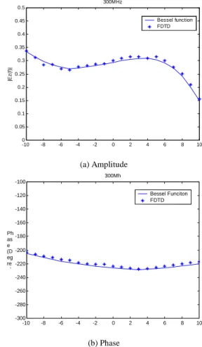
In order to test our FDTD algorithms, a plane wave interacting with an object is simulated in this section, shown in Fig 6. Without loss of generality, the object structure is specified as dielectric cylinder. The reason for using dielectric cylinder is there exist an analytical solution to this problem. The field resulted from a plane wave at a single frequency interacting with a dielectric cylinder can be calculated through a Bessel function expansion [15]. This will give us an opportunity to check the accuracy of FDTD simulation used here.
Fig 6 Verification Case of FDTD Method: Plane Wave Impinging on the Dielectric Cylinder
This simulation of a plane wave pulse hitting a dielectric cylinder with diameter of 20cm and dielectric parameters of
30
=
r
ε
andσ
=
0
.
3
is shown in Figure 7. After 25 time steps the plane wave has started from the side; after 50 time steps, the pulse is interacting with the cylinder. Some wave passes through the cylinder, and the remaining is diffracted. After 100 time steps, the main part of propagating pulse almost passes through computational region.The analytical solution can be calculated using the Bessel function expansion. Details of calculation can be found in L. Harrington’s book [15]. -10 -8 -6 -4 -2 0 2 4 6 8 10 0 0.05 0.1 0.15 0.2 0.25 0.3 0.35 0.4 0.45 0.5 300MHz |E z (f )| Bessel function FDTD (a) Amplitude -10 -8 -6 -4 -2 0 2 4 6 8 10 -300 -280 -260 -240 -220 -200 -180 -160 -140 -120 -100 300Mh Ph as e (D eg re ) Bessel Funciton FDTD (b) Phase
Fig 7. The Comparison of FDTD result vs. Bessel function expansion result along the propagation center axis of cylinder at two frequencies. The cylinder is 20 cm in diameter and has relative dielectric constant of 30 and a conductivity of 0.3 S/m.
Here the cylindrical coordinates are used, but in z direction it F is same as the previous coordinates./
Figs. 7(a) and 7(b) show a comparison of FDTD calculated results with analytic solutions from Bessel function expansions along the center axis of the cylinder in the propagating direction at 300 MHz. The simulation was made with a program attached in Appendix. The accuracy is quite good (less than 2%)
Plane Wave
Center Axis
V. SIMULATION RESULT
A. Simulation 1: Separation Distance Effect on 20H Rule
Simulation 1 is aimed at finding some relationships or effects of different separation distance when the 20H rule is implemented. Structures with different separation distances are tested. In this part, a dipole sinusoidal excitation source is used. Different with the uniform voltage excitation source, the dipole source will not change with separation distance. This property is conductive to compare various functions when different separation distances are using.
In our simulation, the PCB plane Length is fixed as L = 2 cm, Excitation source is selected as:
)
2
sin(
10000
fkdt
E
center=
π
where f = 600 MHz, k is time step in FDTD algorithms and dt is
∆
t
=
1
.
667
×
10
−13 (s).The simulation results are listed in the following table:
TABLE 1
THE SIMULATION RESULTS FOR FIRST STRUCTURE
L (cm) h (mm) n (d=nh) P (
10
−12W
) 2 0.2 0 0.5531 2 0.2 10 0.4002 2 0.2 20 0.0565 2 0.4 0 0.1949 2 0.4 10 0.3049 2 0.4 20 0.2786 2 0.6 0 0.1875 2 0.6 10 0.2421 2 0.6 20 0.2936From data we collected, when d = 0.6 mm, extending ground plane by 20H rule will increase the radiation. Actually the radiation in this case is much stronger than that of the original structure. Same as h = 0.6 mm, Radiation will increase after applying 20H rule. Compared with simulation results where h = 0.4 mm, the radiation in original structure also increases given that excitation sources in two cases are the same. As a conclusion, the separation distance in PCB strongly affects implementation of the 20H rule. When ground plane and power plane come closer, there will be more energy radiating out of PCB. When the separation distance change, regardless of effect of frequency, 20H rule will have different effects on radiation. Hereby, we should notice that this conclusion is based on the presumption “at the same frequency since frequency will strongly change effect of PCB radiation properties, which we will see in next section.
B. Simulation 2: Frequency Effect on 20H Rule
Simulation 2 is based on frequency test for 20H rules. In this section, effects of PCB length on the 20H rule will be considered. Here, the uniform voltage sources are used. For ease of comparison, excitation sources are set as
)
2
sin(
1000
fkdt
E
line=
×
π
.Our separation distance is fixed in this simulation as h = 0.4 mm. According to discussion in previous sections, the voltage of our excitation source can be obtained. In our simulation, V = 0.6 (V). Radiation for structure L=4cm, d=0.4mm is simulated for different frequency:
TABLE 2
THE SIMULATION ABOUT DIFFERENT STRUCTURE FOR DIFFERENT FREQUENCY L (cm) h (mm) f (MHz) n (d=nh) P (
W
1010
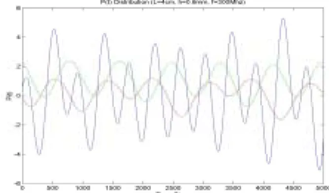
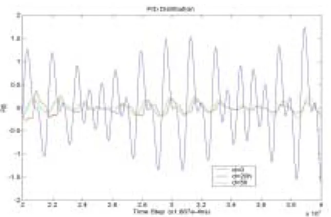
− ) 4 0.4 300 0 1.152 4 0.4 300 5 0.692 4 0.4 300 10 0.603 4 0.4 300 15 0.603 4 0.4 300 20 0.602 4 0.4 900 0 1.035 4 0.4 900 5 1.023 4 0.4 900 10 1.017 4 0.4 900 15 1.021 4 0.4 900 20 1.023At the same time, in addition to quantitative expression of radiation, P(t) for different extending distances (d = nh) is simulated and plotted in Fig 8 and Fig 9. For f=300MHz, value of P(t) for d = 0, d = 5h, d = 20h are presented by red, green and blue line, respectively, in Fig 8. When d = 0, P(t) has very strong resonance than the other two. When d = 5h, the resonance is reduce by a huge amount, and when d = 20h, it almost disappear. Refer to the table, it can be seen that when d = 0h, P is very big, but when it reach d = 5h, it decreases by almost 40%, if we further extend ground plane, the radiation will decrease slightly. After d = 15h, changes in amount of P are really small.
Fig 8.Poynting Vector in Time Domain (f=300Mhz, L=4cm, h=0.4mm)
P(t) for the same structure at frequency 900 MHz is shown
in Table 2 and Fig 9. The Poynting vector for d = 20h (blue curve) also has some resonance. When d =5h, P(t) is similar to that when d = 0. Refer to the Table 5, the radiation when d = 0 is highest among all. The radiation will decrease if the ground plane is extended. When d = 5h, the radiation decrease by almost 60%. When we further extending ground plane, the radiation continue to decrease. After d = 15h,.there are just slight changes in decrease of radiation The radiation energy calculated in one time period has the same properties.
Fig 9 Poynting (Vector in Time Domain (f = 900MHz, L = 4cm, h = 0.4mm)
Other simulation for other different structure frequency are also got as below:
TABLE 3
SIMULATION RESULT FOR DIFFERENT FREQUENCY f n (d=nh) P
(
10
−10W
)
150 0 0.6901 150 5 0.4345 600 0 4.721 600 5 3.591 900 0 1.868 900 5 0.432From above simulation, both the dimension L and frequency
f for different structures are considered. The results show that
frequency and length of PCB will also affect 20H rule implementation mainly through resonance caused inside PCB. When L is large, it is easy to cause great amount of resonance even when not very high frequency, as shown in the case L = 6 cm, f = 600 MHz.
VI. CONCLUSION
In this paper, one of PCB design techniques, the 20H rule, is applied in the simulation by the FDTD method. According to simulated results, some useful conclusions are drawn. The 20H PCB design rule will change field distribution along structure. Originally, field distribution is symmetric, both vertically and horizontally. After using 20H rule, field will concentrate more on the upper half space.
The effects of the 20H rule will highly depend on three factors, namely, operating frequency, length of PCB and separation distance. The operating frequencies play an important role on the 20H rule because it also affects function of the other two factors. So the normalized length and separation distance with regarding to wavelength should be used to compare their relationships with each other. For our case studies in which the frequency and the length are fixed, smaller separation distance strengthens the function of the 20H rule. Also in our case studies, higher frequencies are found to cause resonance problem. In this sense, effects of the 20H rule are determined by some specific conditions. More explorations
are expected so as to gain more physical insight into this design rule.
APPENDIX
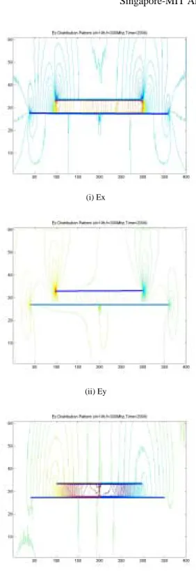
A. Radiation Patterns Before and After Appling 20H Rule In Different Structures.
(1) L = 2cm, d = 0.6mm and f=300 Mhz
(i) Ex
(ii) Ey
(iii) Hz
(i) Ex
(ii) Ey
(iii) Hz
Fig 10 (b) Radiation Pattern After Applying 20-H Rule
REFERENCES
[1] Mark I. Montrose, Printed Circuit Board Design Techniques For EMC Compliance, New York: IEEE Inc., 1996
[2] Mark I. Montrose, EMC and Printed Circuit Board Design Design
Theory, and Layout Made Simple, New York: IEEE press, 1999
[3] I.A. Weinstein, The Theory of Diffraction and the Factorization Method (Generalized Wiener-hopf Technique), Boulder: Golem Press, 1997
[4] Dr. Zorica Pantic-Tanner & Franz Gisin, Radiation from Edge Effects in Printed Circuit Boards, Santa Clara Valley Chapter of EMC IEEE
Society, May, 2000
[5] Yee, K.S., “Numerical solution of initial boundary value problems involving Maxwell’s equations in isotropic media”, IEEE Trans. Antennas and Propagation, vol.14, no. 124, 1996, pp. 302- 307
[5] Taflove, A. and M.E. Brodwin, “Numerical solution of the steady-state electromagnetic scattering problems using the time-dependent Maxwell’s equations ”, IEEE Trans. IEEE Microwave Theory and
Techniques, vol. 23, no. 1975, pp. 623-660
[6] Taflove, A., “Review of the formaultion and applications of the finite difference time-domain method for numerical modeling of electromagnetic wave interactions with arbitrary structures,” Wave
Motion, vol. 10, 1998, pp. 547-582
[7] Holland, R.L, “Threde: A free-field EMP coupling and scattering code,”
IEEE Trans. Nuclear Science, vol. 23, 1975, pp. 547-582
[8] Holland, R.L., “Finte-difference analysis of EMP coupling to lossy dielectric structures,” IEEE Trans. Electromagnetic Compatibility, Vol. 22, 1980, pp. 203-209
[9] J.P. Berenger, “ Perfectly matched layer for the FDTD solution of wave –structure interaction problems”, IEEE Trans. Antennas and
Propagation, vol. 44, No.1 1996
[10] J.P. Berenger, “Improved PML for the FDTD solution of wave structure interaction problems”, IEEE Trans. Antennas and Propagation. Vol. 45, No.3 March 1997
[11] K. S. Kunz, and R J. Luebbers, The Finite Difference Time Domain
Method for Electromagnetic, Boca Raton, FL: CRC Press, 1993
[12] D.M Sullivan, A Simplified PML for use with FDTD Method, IEEE
Microwave and Guided Wave Letters, Vol.6 1996, pp. 97-99
[13] D.M.Sullivan, An unsplit step 3D PML for FDTD Method, IEEE
Microwave and Guided Wave Letters. vol. July 1997, pp. 184-186
[14] R. Harrington, Time Harmonic Electromagnetic Fields, New York: McGraw-Hill 1961.
[15] Britt, C.L. “Solution of Electromagnetic Scattering Problem Using Time domain Techniques”, IEEE Trans. Antennas and Propagation, vol37. 1990, pp. 919-927
[16] Yee, K.S. D. Ingham, K.Shlager, “Time-domain extrapolation to the far field based on FDTD Calculations”, IEEE Trans Antennas and
Propagation, vol 37, pp. 919-927
[17] K.S.Yee, “Numerical Solution of Initial Boundary Value Problems Involving Maxwell’s Equations in Isotropic Media”, IEEE Trans. On
Antennas and Propagation, vol. AP-97, 1999, pp.585-589
[18] A.Taflove, Computational Electrodynamics: The Finite Difference
Time Domain Method for Electromagnetics. Boston: Artech House,
1995
[19] Dennis M. Sullivan, Electromagnetic Simulation Using the FDTD
Method, IEEE Press series on RF And Microwave Technology, New
York, 2000
[20] N. N. Rao, Elements of Engineering Electromagnetics, Prentice Hall, Englewood, New Jersey,1994
[21] Chen, Huabo; Fang, Jiayuan, “Effects of 20-H rule and shielding vias on electromagnetic radiation from printed circuit boards”, IEEE Topical
Meeting on Electrical Performance of Electronic Packaging, 2000,
Pages 193-196
[22] Daura Luna F., “Multiboard printed circuits and electromagnetic disturbances. 2”, Revista Espanola de Electronica, Issue 510, 1997, pp. 72-76, 80
[23] Zhou, D. Huang, W.P.; Xu, C.L.; Fang, D.G.; Chen, B, “The /perfectly matched layer boundary condition for scalar finite-difference time-domain method”, IEEE Photonics Technology Letters, vol 13, Issue 5, 2001, Pages 454-456 .
[24] Rogier, H.; De Zutter, “D. Berenger and leaky modes in microstrip substrates terminated by a perfectly matched layer”, IEEE Transactions
on Microwave Theory and Techniques, vol 49, Issue 4, Part 1, 2001, pp.