The Design and Implementation of an I/O Controller
for the 386EX Evaluation Board
by
Marcus-Alan Gilbert
Submitted to the Department of Electrical Engineering and Computer Science in Partial Fulfillment of the Requirements for the Degree of Master of Engineering in Electrical
Engineering and Computer Science at the Massachusetts Institute of Technology May 1995
Copyright © 1995, Marcus-Alan Gilbert. All rights reserved
The author hereby grants to M.I.T. permission to reproduce and to distribute copies of this thesis document in whole or in part,
and to grant others the right to do so.
Author , (C 'U f' • • -.
Department of Electrical Engineering and Computer Science - May 19, 1995 Certified by. _
I
\i.
Accepted by Richitil DAThornton rvisor F.R. MorgenthalerChairman, Department Com•tte on Graduate Theses
1MASSACHUSETTS INSTITUTE OF TECHNOLOGY
AUG 1 01995
LIBRARIES
The Design and Implementation of an I/O Controller
for the 386EX Evaluation Board
by
Marcus-Alan Gilbert
Submitted to the
Department of Electrical Engineering and Computer Science
May 18, 1995
ABSTRACT
This report describes an extension of the development system for MIT's Microprocessor Design Lab, course 6.115. The current development system for 6.115 is the 386 EX
evaluation board. The current development system has been extended by having the 68HC 11 microcontroller control peripheral devices. The original intention was to develop such a system around the PowerPC line of processors, however the availability of the 386EX evaluation board, and its adoption into 6.115 led to its being the choice for the extension. The results of this initial development work are the creation of a
microprocessor based system that is capable of processing data directly from an analog to digital converter under 68HC1 l's control. The software development has been done in C, 80x86 assembly, Max-Forth, and 68HC11 assembly. This report also includes sections that extend the prototype system to a PowerPC implementation.
Thesis Supervisor: Richard D. Thornton
Table of Contents
1 Introduction 1
2 Background 4
3 The Peripheral Processor 6
3.1 68HC11 Evaluation Board -NMIX/T-0020 68HC11 6
3.2 The 68HC11 microcontroller 11
3.2.1 The 68HC11 Functional Units 11
3.2.2 The Synchronous Serial Peripheral interface Unit (SPI) 11
3.2.3 The Serial Communications Unit (SCI) 12
3.2.4 The Analog to Digital Converter 13
3.2.5 The Parallel Ports 14
3.2.6 The Central Processing Unit 16
3.3 The PC Connection 16
4 Analog Anti-Aliasing Low Pass Filter 17
5 The Host Processor Section 18
5.1 Memory 19
5.1.1 Programming Flash Memory 20
5.2 Peripheral Connectors 20
115.3 PC/104 Bus 20
5.4 Programmable Logic devices 21
5.5 Asynchronous Ports 21
5.6 386 EX 22
5.6.1 Parallel Ports 23
5.6.2 DMA Unit 24
5.6.3 Chip Select Unit 24
5.6.4 Interrupt Control Unit 24
5.6.5 The Analog Devices 7847 25
6 System Software and Algorithms 26
6.1 68HC11 Routines 27
6.2 386 EX Register Initialization 30
6.3.2 Correcting for Errors in the Output Signal 38
6.3.3 Testing the DSP Algorithms 40
6.4 Putting it all Together 44
7 System Enhancements 46
7.1 Analog to Digital and Digital to Analog Enhancements 46
7.2 Peripheral Processor enhancements 46
7.2.1 The 68HC16 47
7.2.2 The 8051 47
7.2.3 The Need for Two Asynchronous Ports 47
7.3 Host Processor Enhancements 48
7.3.1 The PowerPC 601 48
7.4 Other issues 49
7.4.1 DMA 49
7.4.2 Serial as Opposed to Parallel Operation 49
7.4.3 Improving the Software 50
7.4.4 Programming the EPROM 50
8 Alternative Methods 51
8.1 Academia 51
8.1.1 University of Alberta 51
8.1.2 Rensselaer Polytechnic Institute 52
8.1.3 A Simulator for Teaching 52
8.2 Equipment 52
8.2.1 Hardware 52
8.2.2 Alternative Software 53
9 Results and Conclusion 54
10 Acknowledgments 56
11 Appendix 57
11.1 References 58
11.2 Contact Personnel 61
11.3 68HC11 Register Descriptions 64
11.4 386EX Register descriptions 65
11.6 68HC11 Memory MAP 67
11.7 Code Listings 68
List of Illustrations
Figures
Figure 1: A Microcontroller Controlling Data Flow from Three peripherals to the Host
processor
Figure 2a: Mode 1, Code Load Figure 2b: Mode 2, Data Acquisition
Figure 3: The NMIX-0020 Evaluation Board Figure 4: DB9 to J6 Connections
Figure 5: The J5 to LS244 to J2 Connections
Figure 6: Effective Decoder Selections, with Jumpers A and B in: a) 8K
b) 16K
c) 32K position
Figure 7: DB9 Connection from PC to Evaluation Board Figure 8: The Sallen-Key Circuit
Figure 9: Desired Frequency Response
Figure 10: The 386 EX Board Functional Units Figure 11: DB9 with Rx and Tx Connections Swapped Figure 12: The 386EX Functional Components
Figure 13: Parallel Port Connection to D/A Figure 14: 7847 In Uni-Polar Mode
Figure 15: Latch Control Logic for the 7847 Figure 16: Discrete Time Frequency Responses Figure 17: Continuous Time Frequency Responses Figure 18: Fixed Point Filter Coefficients
Figure 19: Redesigned Low Pass Filter
Figure 20: a) An example of Over and UnderShoot b) Output after Adjustment
Figure 21: The Frequency Responses of the Uni-Polar (DC Added) Test Vectors Figure 22: The 386 EX Program Flow Chart
Tables
Table 1: DB9 to J6 Connections and Signal Names Table 2: Software Tests without Board
Table 3: Software Tests with Evaluation Board
Table 4: Software Tests with Evaluation Board Connected to the 68HC11
Code Samples
Example 1: 68HC 11 Register Initialization Example 2: A Forth Word Definition
a) with a built in assembler
b) without an assembler
Example 3: Enabling the Expanded I/O Addresses Example 4: An Array of Floating Point Coefficients Example 5: An Array of Fixed Point Coefficients
Notational Convention Guide
Most of the text in this document will appear in the default text font however there will be certain instances where this is not the case. These include:
Register Names and Signal Names will appear in caps such as, REMAPCONFIG, AN1. Active low signals will have the '/' character. For example, /WE.
Data values and memory addresses will use this font OxFF. Hexadecimal numbers will appear as Oxdd, where d is a hex digit. Binary Numbers will be pre-pended with Ob as in Ob 1110 .
References to the World Wide Web will appear in italicized font,
http://www.powerpc.com.
When a World Wide Web Site appears in the reference section the following format will be used.
<Author's last name, Author's first name (if known)>. <Title as it appears at the top of the browser window> <URL>,<Year of last known modification>.
Usenet newsgroups will be designated by the following font: comp. arch. embedded
Source code will appear as such: for (i=0; i<7; i++)
When specific code variables are referred to in the text they appear in italicized font,
x_buffer.
1
Introduction
This report describes current work toward a hybrid development system based on MIT's Microprocessor Project Lab, 6.115. The current development work focuses on extending the current development system, which is centered around the 386EX
processor. The purpose is to use the microcontroller to pass data to the processor so that it can execute a data processing algorithm.
The current development system for 6.115 utilizes the 386 EX evaluation board. This has been a substantial improvement over the previous HP64000 system. The current
system provides a contemporary development platform from which students can learn to use microprocessors. Current development has concentrated on a design objective that
attempted to accomplish one goal, to create a system that is suitably generic to allow different host processors to be utilized in development. The first of these goals has been realized with the advent of the new development system. However, much of the work this term has focused on the second of these goals.
To create a system that is suitably generic to allow different host processors to be utilized, we have chosen to use the following approach. We have a low-cost
microcontroller to handle I/O and data collection and have the main processor process the data (see figure 1). The original intent was to have the host processor be from the Power PC family. With the Power PC, we have a processor that is suitably fast to execute DSP algorithms comparably to DSP processors. However, because of its availability and it design for embedded applications, the 386 EX was chosen as the host processor. The 68HC 11 provides the peripheral micro-controller functions for the new
Figure 1: A Microcontroller Controlling Data Flow to the Host processor
development system. The 68HC 11 was chosen for the abundance of software and cross development tools available. It was also chosen for the availability of on chip peripherals including RAM, ROM, asynchronous ports, and an Analog to Digital Converter (A/D). The 68HC 11 Evaluation Board (EVB) that was used in the prototype development system contains an RS-232c level converter, several connectors, a small proto-board in addition
to glue logic and system memory.
Originally there were supposed to be two modes of operation: code load, and data acquisition. In code load mode the peripheral micro-controller programs the host
processors' ROM with instructions downloaded from the PC (see figure 2a). The host PC would connect to the 68HC 11 via the comm port. With the advent of cross-development tools available for the PC it is feasible that the user can write and compile the program on
the PC and then transfer the Intel Hex file from the PC to the development system even if the target is of a different processor family'. This mode does not appear in the current
development system because of the code size necessary to hold the HEX file and calculate its checksum. (See System Enhancements)
I Alternatively, one could use a development system that has the same processing core as the target
system. The main advantage to this being that the user need not worry about compatibility across platforms, and further run-time errors could be substantially reduced by running the program on the host computer.
1. Hex File Downloaded 2. Hex File programmed
via PC Comm Port tnrough 386EX Comm
Port 2
68HC1 1Evaluation 386 EX Evaluation
Board Board
Figure 2a: Mode 1, Code Load
Figure 2b: Mode 2, Data Acquisition
In the data acquisition mode, the peripheral microcontroller provides data for the host microprocessor to manipulate (see figure 2b). The 68HC11 connects to the 386 EX evaluation board via the 386 EX expansion bus. It is conceivable that the host
microcontroller would access other processors in a similar manner. For this
implementation the data source is the Analog to Digital Converter contained within the 68HC 11. The current design is meant to be flexible enough to allow the utilization of other peripherals and not meant to be restricted to the A/D. After the 386 EX has processed the data it sends the calculated output to the AD 7847 Digital to Analog Converter.
The following section further describes some of the background leading to the creation of the prototype system. Section 3, describes the operation of the 68HC 11 evaluation board, section 4 details the anti-aliasing low pass filter. Section 5 discusses the implementation of the 386EX and its evaluation board and the operation of the 7847 under the control of the 386 EX, section 6 highlights the software written for the system and explains the DSP algorithms used to test the development system. Section 7 suggests
possible alternatives and enhancements to the development system including those implementations that use the PowerPC 601. Section 8 mentions other microcontrolled applications in both industry and academia.
2
Background
The previous system under use in 6.115 lab was the HP-64000-UX Microprocessor Development Environment system. The system included the 68000 in-circuit emulators and diskless, networked HP workstations. The performance was suspect to say the least, although development was done the proven architecture of the 68000, the supporting
workstations were slow and suffered from intermittent crashes. In addition, the former system was archaic and costly to maintain. The emulation pods were beginning to show signs of wear from repeated use. Also under the former system it was necessary for students to hand wire the peripheral components, which led to wasted time correcting wiring mistakes. This time could be better spent doing useful hardware and software development. In addition to wasting time doing mindless hand wiring, students were not exposed to microprocessors of contemporary design (e.g., 68030, '040, 386). The 68000 has been a formidable design that has been around for well over a decade, however
students in the 6.115 class were not being exposed to current development tools and more recently designed microprocessor architectures2. At the end of 1993 it was clear that a
solution utilizing current hardware was necessary. [1]
Although microprocessor designs and development tools have changed rapidly in the recent years, the objectives of the course have remained the same. The current and former objectives of 6.115 are, as reported in the Course plan: Hardware Engineering, Software Engineering, and Technical Skills. The current development system, the 386 EX evaluation board allows students to satisfy these goals while relieving students of the tedious tasks involved with hand wiring a system. The specific details of such a newer system are currently being investigated, however one of the essential
2 It should be noted however, that the experiences with the HP development system are the result
of our use of an out of date system and not a reflection of HP's inadequacies in the microprocessor
development arena. In fact a newer version of the 64000 system has been proported to be more than adequate for development purposes. See the industry reference section.
components of an autonomous system is the capability to download programs from various sites, presumably PCs.
With this background, development work during the spring of 1994 utilized the existing HP64000 system to create a microprocessor based EPROM programmer capable of running programs downloaded from the PC. The evaluation system consisted of three sub-systems, the Microprocessor and lower memory, the multi-function peripheral, and the upper (EPROM) memory. The distinction between upper and lower memory is that lower memory contained instructions and data necessary to program the upper memory EPROM. Lower memory also contained the necessary vector to begin instruction
execution at the upper EPROM's (memory mapped) address. It was originally planned to extend such a system from a 68000 based system to a 68040 (and possibly beyond) to even a 80x86 based system capable of downloading and subsequently running programs in embedded applications. [2]
During the fall of 1994, the microprocessor design lab received 386 EX evaluation boards and several Pentium systems. With the presence of an up to date development platform the design objective had to be changed from one of the construction of an immediate system to an objective that seeks to have an extendible architecture that can evolve to include newer microprocessors as the appear.
According to B. Furht and the W.A Halang in A Survey of Real Time Systems the next generation of real-time systems will be based on open systems. They assert:
Open real-time computer concepts are based on hardware architectures which use off-the-shelf standard microprocessors, standard real-time operating systems, standard communications protocols, and standard busses.
With this perspective in mind, the author has sought to create, and illustrate how one might design a generic system. [3]
There still exists a need to continually improve the microprocessor project lab with current processors and allow for an open architecture for other processors. To this end, we contemplated doing development work with the PowerPC line of RISC architectures. The current set of RISC architectures and modern microprocessors can execute DSP algorithms suitably fast. Modern CISC architectures are also reported to perform native
signal processing. [4][5] The first of the PowerPC processors, the 601, was released in 1992. There is beginning to be a abundance of development tools for the 601 (see Alternative Equipment). Specifically, the author would have liked to obtain the 601 System Design Kit with its associated peripherals. Unfortunately, time and finances did not allow us to use such a system. Future development work, should be aimed at obtaining such a system. [6] [7]
The focus here has been to extend the 386 EX evaluation board to a system in which a peripheral processor controls I/O, in the form of signal data. There are a large number of systems that utilize such an approach as to use one or more microcontrollers for peripheral processing and to utilize a more powerful CPU for core processing. It is hoped that the 386EX- 68HC11 system can be further developed into other systems such as a PowerPC-68HC11 system.
3
The Peripheral Processor
The peripheral processor section consists of a 68HC11 evaluation board and two LS244 Octal buffers. The 68HC11 evaluation board contains the necessary level converters and peripheral chips to allow connection to the PC (via a DB9 connector and serial cable) and to 386 EX expansion bus. The LS244 buffer provides the signal strength to drive data onto the 386 EX expansion bus.
3 .1 68HC11 EVALUATION BOARD -NMIX/T-0020 68HC11
The NMIX/T-0020 68HC11 evaluation board contains the 68HC11, RAM, level converters, glue logic, and a prototyping area. It also contains connectors for an LCD display and a 4x5 keypad interface. The board was purchased from New Micros, Inc. (see 68HC11 FAQ). The board has three 28 pin JEDEC (Joint Electronic Devices Engineering Council) sockets, and several connectors. The connectors that were used in
Figure 3: The NMIX-0020 Evaluation Board
The J6 connector is used for serial communication between the host PC and the 68HC 11 evaluation board. The J6 connector is attached to the DB9 connector as shown in figure 4. Pins 5 and 6 provide serial out and serial in, respectively. Pin 8 provides the case and electrical grounds. The Clear to Send (CTS) and Request to Send (RTS) signals from the PC are tied together. The Data Terminal Ready (DTR) and Data Select Ready (DSR) from the PC are also tied together (see PC section).
J6A
)C0
nectorSedal Data From 68HC11 EVB
Serial Data to 68HC11 EVB
DB9 Connector Figure 4: DB9 to J6 Connections J5 Connector on 68HC1 1 FVR J2 Connector on the 386 FY FVR
Figure 5: The J5 to LS244 to J2 Connections
J3 8K RAM 8K EEPROM BASIC ROM (Optional) ICL232
I
J4 J6 r I I IThe J5 connector provides data for the 386 EX evaluation board. Three of the 68HC 11's Parallel ports are connected to the J5 connector. These parallel ports can be used as either inputs or outputs. These include Ports A, D, and E. Port D and A are used to provide data for the 386 EX evaluation board, in data acquisition mode. The connector pins 3-6 on J5 (which represent Port D) connect to the expansion bus of the 386 EX and provide the lower nibble of data. Connector pins 7, 8, 12, 13 , which represent Port A bit 3, 4, 6, and 7 respectively, form the higher nibble of data (see figure 5). Port A also provides the status signal for the indication that an A/D conversion has completed and the sample is ready. Port A pin 3 provides the active high, RDY signal. Port E pin 1, of the J5 provides the analog input signal for the internal A/D.
The output signals from the 68HC11 can only sink 1.6 gA to ground while preventing the package pin from rising above logical level zero, or .4 V. Similarly the 68HC11 can only source .8 gA at the logical one value of 4.5 V. These current levels are only sufficient enough to drive one TTL gate. Consequently an LS244 octal buffer has been added to provide adequate signal levels for the 386 EX evaluation boards.
Level conversion from the High Density Complementary Metal Oxide
Semiconductor (HCMOS) signals to TTL levels is accomplished via the ICL232. The ICL232 provides the receiver/ transmitter pair for the serial in and serial out for
connection to the PC. There is an additional receiver/transmitter pair that can be utilized for the serial communication (for Programming the Flash Memory) of the 386 EX EVB. For RS232C communication the logical one is represented by a -3V to -15V signal, conversely a logical zero is represented by a 3V to 15V signal. The ICL232 Vdd and V,
supply voltages are 5V and OV respectively, the higher voltages for RS232 communication are generated via an internal charge pump.
Glue logic provides the chip selects for the three 28 pin JEDECS. The three 28 Pin JEDECS occupy slots U3, U4, U5. Theses slots are used to provide the additional RAM, EPROM, and ROM respectively. The chip selects for the sockets are generated by the 74HC 138. When the jumpers A and B are in the 8K position, all three address lines are brought to the decoder. This means that each of the eight generated chip selects
represent a single 8k byte segment out of the 64K memory map. When jumpers A and B are in the 16K position, address lines A15 and A14 are brought to the decoder. The A13 address line is held high. This means that the upper four generated chip selects represent a single 16K byte segment out of the 64K byte memory map. When jumpers A and B are in the 32K position, address line A15 alone controls the part. The A14 and A13 lines are held high. Each of the two upper chip selects represent a 32K byte segments out of the 64K memory map. [8]
a) b)
Figure 6: Effective Decoder Selections, with Jumpers A and B in: a) 8 K b) 16 K c) 32 K position
There are two other signals that control the decoder: Address Strobe (/AS) and the on board memory Disable (IMEMDIS). The /AS signal must be active low before any chip selects are enabled. This is the processor's signal indicating the address on the bus is valid for the off-chip memory. The /MEMDIS signal allows an off-board open collector source to disable the on board decoder, so off board components can usurp a memory segment from on board memory, even if the entire 64K is filled with RAM on the main board.
For this implementation, the default 8K addressing scheme was utilized, which required A and B jumper settings to be set in the 8K configuration. It was decided that the Forth language would be used, thus nullifying the need for external ROM memory. This configuration allows a user program to reside in EEPROM memory.
The 68HC11 EVB communicates with the PC through the comm port as shown in see figure 7.
-D B9Caib
I-srssrr---I
::'::::''
E
::uhimmhiii::
":':
I:
' t L:
::::::::.:::::·::;·:-
···--
:::
:::::
··
·.::_
Figure 7: DB9 Connector attachment from PC to Eval Board
Data Carrier Detect Receive Data Transmit Data Data Terminal Ready Signal Ground Data Set Ready Request To Send Clear To Send No Connection DCD Rx Tx DTR GND DSR RTS CTS NC 1 2 3 4 5 6 7 8 9
Table 1: DB9 to J6 Connections and Signal Names 3 .2 THE 68HC11 MICROCONTROLLER
The 68HC11 microcontroller was chosen as a host processor because of its simple instruction set its availability of on-board peripherals, specifically an on-board analog to digital converter (A/D). There is also an abundance of hardware and software
development tools available for this microcontroller. The 68HC11 is an 8-bit data, 16-bit address microcontroller. The instruction set is similar to earlier 68xx designs. Depending on the flavor the 68HC11 (denoted by the suffix or prefix, i.e. 68HC11 ) there are a
7 6 8
Im
---variety of on chip peripherals that are available. These include EEPROM/OTPROM (One Time programmable read only memories), RAM, digital I/O, timers, synchronous and asynchronous communication channels and an A/D converter. The board from New Micros uses the F68HC11FN. The 68HC11 Frequently Asked Questions (FAQ) describes the different flavors of the 68HC11. The F68HC11FN was produced by Motorola specifically for New Micros. The F68HC11FN is functionally equivalent to the 68HC1 1E9. This flavor of the 68HC1 1 contains 8 Kbytes ROM which contain the Max-Forth Kernel, 256 bytes of internal RAM, an 8 bit 8 channel A/D, 1 synchronous serial port, and 1 asynchronous serial port. [9]
There are four modes of operation of the 68HC11, these include: single chip, expanded, multiplexed, special bootstrap and special test. Single-chip mode allows the microcontroller to run with out external data paths. The New Micros Board has configured the 68HC11 to run in expanded, multiplexed mode. This mode allows the microcontroller to access off-chip devices. It provides an external data and address bus. The other two modes are special variations on the first two modes.
3 .2.1 The 68HC11 Functional Units
The functional units of the 68HC11 include: the Synchronous Peripheral Interface (SPI), the Serial Communications Interface (SCI), the A/D, EEPROM, the Parallel ports and the Central Processing Unit. The SPI provides the protocols necessary for synchronous communication with the peripherals. The Serial Communications Interface could provide the signals for serial communication with the 386 EX during code load mode and is also used by the Max-Forth Kernel. The parallel ports provide the data and control signals for the 386 EX during data acquisition mode. The A/D digital converter converts the
continuous time input waveform to discrete time digital signals. The Central Processing Unit would provides the arithmetic ability necessary for the calculation of the HEX file checksum during the code load mode, and executes the instructions necessary to control the A/D during data acquisition mode. The following sections provide a brief overview of each functional unit and its associated registers.
The synchronous serial peripheral interface is one of the two serial communications channels on the 68HC 11. The subsystem allows the 68HC 11 to communicate with synchronous peripherals. The SPI provides fully duplex transfers as data can be both shifted in and shifted out on the two different serial lines. For this implementation, the SPI is not currently used. However, the SPI unit could be used to transfer data from a
synchronous serial A/D such as the Analog Devices 7869 (see Section 7). This would utilize the MISO (Master In Slave Out) and MOSI (Master Out Slave In) pins which are also the Port D pins PD3 and PD2. The SCK and /SS pins which are pin PDO and PD1, would also be used in this sort of implementation.
The serial peripheral unit is basically a shift register. The SPI synchronous clock register (SCK) controls how the bits are shifted out at what phase relative to the clock. There are four different combinations of the serial clock phase and polarity. These include the four combinations of clock high/low and polarity/zero. If clock high is selected, the data is transmitted in (out) on the low to high transition of SCK, conversely if clock low is selected data is transmitted on the high to low transition. The polarity designation has to do with the placement of the bits relative to the assertion of the /SS signal.
3 .2.3 The Serial Communications Unit (SCI)
The serial communications unit provides asynchronous communications with the 68HC 11. The SCI is a fully duplex UART, that uses NRZ (non-return to zero) format. The NRZ format utilizes one start bit, eight or nine data bits and one stop bit. The synchronous communications unit, is controlled by five registers: BAUD, SCCR1, SCCR2, SCSR, and SCDR. Port D lines 1 and 0 provide the transmit (Tx) and receive (Rx) signals respectively, for the serial communication unit.
The BAUD register selects the baud rate for asynchronous communications and contains a couple of bits for factory testing.
The SCCR1, or SCI control register 1 has three bits associated with the 9 bit data transmit format. The WAKE bit selects in which manner the receiver will wake up. The remaining 4 bits are reserved and have no function.
The SCCR2, SCI control register 2, contains most of the SCI controls. The most significant four bits control the enabling of interrupts for the SCI interrupts. An interrupt can occur when a transmission buffer is empty, a transmission completes, when the receive buffer has been filled or the Rx line has become idle. Idle is defined as the line staying at a logic level 'high' for the duration of the transmission.
The SCI status register provides information with regard to conditions in the reciever/transmitter. The SCI status register tells whether or not: the transmit data register is empty, if the transmission has completed, if the receive data register is full, an idle line has been detected, or whether data has overrun the receive register. Framing errors and noise detection are also reported in the status register.
The SCI data register is a dual function register that provides a location to write data to be transmitted and read data to be received. Writing to this particular address, 0xB024, accesses the Transmit Data register, whereas a read to this address accesses the Receive Data register.
The Max-Forth kernel uses the SCI for communication with the PC. It enables the SCI and sets the Baud Rate to 9600 baud. It is therefore necessary for the I/O routines for the Max-Forth Kernel to be remapped in order to serially communicate with the 386 EX in mode 1. It is also necessary to reset the baud rate to 19200. (See section 7)
3 .2.4 The Analog to Digital Converter
The 8-bit, 8-channel Analog to digital converter on the 68HC11 provides the data for the 386 EX to process. The A/D is a successive approximation type. The A/D timing is synchronized with either the system E clock or with the internal oscillator. The A/D conversion takes about 32 E clocks. This implementation uses the E clock with a frequency of 2 MHz. At that clock speed the A/D has a sampling frequency of =_ 62.5 kHz. By the Nyquist criterion, this yields a maximum input signal frequency of 31.25 kHz. To ensure that high frequency signals do not enter the A/D, the input signal is placed on the sampling channel, AN 1 after passing through an anti-aliasing low pass filter (see Anti-Aliasing Filter Section). The Analog to Digital converter is controlled by the A/D control/status register, ADCTL. The ADCTL, selects the mode of operation for the
A/D, selects the channel(s) to be used for conversion, and indicates whether or not a conversion has completed. The operation of the A/D is also effected by the OPTION register. The outputs of the A/D are contained in registers ADR3-0.
The are two different scan modes, and two different channel modes in which the A/D can operate. The first scan mode is continuous in which the A/D continually performs conversions. The second scan mode, is single. In this mode the A/D performs four conversions and then sets the conversion complete flag. No other conversions are performed until the A/D control register is written. The first channel mode is single. In single channel mode conversions are made only from a single channel. In multiple channel mode the conversions are taken from a group of 4 different channels.
In the current implementation, the A/D runs in continuous mode and the data output registers ADR3-ADRO are read successively to obtain the signal values. The data signal is represented as a unsigned fractional result of a comparison with V, and VR. A signal whose voltage of equal value to V,, would yield a result of OxFF in one of the ADR registers. Similarly, a signal whose voltage measured the same as VRL would yield a result of Ox00 in the ADR registers. On the NMIX-0020 board, the V, signal is
connected to Vdd (5V) and the VRL signal is connected to ground. After a signal has been sampled the output value from the ADR registers is passed on to the Port D and Port A data bus (see following Section).
The OPTION register also affects the operation of the A/D. The option register enables or disables the A/D circuitry. This register also selects whether the internal oscillator or the system E clock will be used. In addition this register can select whether or not to have a delay after the A/D starts converting. This delay is used to allow the internal oscillator to stabilize. However this system uses the external E clock and the internal oscillator is not used.
3 .2.5 The Parallel Ports
The 68HC11 has 40 I/O pins, grouped as five 8-bit ports. These five ports have multiplexed functionality. This functionality includes, timers, serial channel, A/D
these pins is determined by a register block. At start up this register block is located at address Ox1000, however the Max-Forth operating system remaps this to address OxB000. There are nine registers that control the five ports (A-E), they reside in locations
OxB000-OxBOOA.
The first port, Port A can be used for general purpose I/O or for use with the timer as a combination of input compares, output captures and a pulse accumulation. When Port A functions as general I/O, the first 3 pins PAO-2 are inputs only, while pins PA4-6 are dedicated outputs. Pin 7 and Pin 3 can be configured as either an inputs or an outputs. The values of these port pins can be accessed by reading the Port A register. Similarly the values on the Port A outputs can be altered by writing to the Port A register. For, this implementation Pin 7 and Pin 3 were configured as outputs.
The Port A pins connected to the J5 connector. The output pins PA7, PA6, PA5, PA4, and provide the higher nibble of the byte wide result from the A/D. PA3, provides the RDY signal for the 386EX to acknowledge (see figure 5).
The next port, Port B can have all of its pins set as general purpose outputs. However in the expanded/multiplexed mode of operations the 68HC11 uses this port for the high byte of the address bus. Consequently Port B is not connected to any of the port connectors and is not used for general purpose I/O.
The pins of Port C, are capable of being configured to be either inputs or outputs. The direction of these pins in controlled by the Data Direction register, DDRC. In
expaned/multiplexed mode Port C takes on the multiplexed role of either the low byte of the address bus or it provides the data bus. Therefore, Port C is also not used for general
purpose I/O.
Port D can be used for either general purpose I/O or it can be used for
asynchronous or synchronous serial communications. The direction of the 6 lower bits is determined by the Port D data direction register, DDDR. The upper two bits of Port D are used for handshaking control for Ports B and C, these bits are unavailable for general I/O. These pins are not connected to J5. The lower two bits PD1, and PDO provide the transmit (Tx) and receive (Rx) signals respectively for the serial control interface. Because Max-Forth uses the SCI for its I/0 routines when communicating with the
terminal, the two bits PD1 and PDO are also unavailable for general 1/O, however they are connected to J5. In this implementation the remaining 4 bits, PD2-PD5 provide 4 bits of data for the sampled value obtained from the A/D.
Port E pins provide either analog or digital inputs to the 68HC 11. These pins can function as either input channels for the internal A/D or they can be used as general purpose digital inputs which can be read by accessing the Port E register. All of the Port E pins are connected to J5. The current prototype system uses Port E pin 1 (also known as AN 1), for the analog signal input to the A/D.
3 .2.6 The Central Processing Unit
The 68HC11 CPU includes two 8 bit general purpose registers (A & B) that can be grouped into one 16 bit accumulator. It also includes two 16 bit index registers, which are used to access memory in index addressing mode. There is also a stack pointer, a program counter and a condition code register. Each instruction consists of an 8-bit opcode
followed by one or more bytes of address/data information. The instruction set of the 68HC 11 includes bit manipulation instructions, 16 bit divide instructions, and exchange instructions.
The A/D access routine was coded in 68HC 11 assembler to take advantage of the performance increase from using assembly language and forego the overhead associated with using Max-Forth. (See software section) [10]
3 .3 THE PC CONNECTION
The PC connects with the ICL232 Level converter via a DB9 connector and cable (See figure 7). The cable connects to the serial port3 of the host PC. A non-handshaking
protocol, in which the CTS (Clear to Send) and RTS (Request to Send) are tied together, has been chosen to transfer data from the PC to the 68HC11 EVB. In this protocol, DTD (Data Terminal Detect), DTR (Data Terminal Ready), and DSR (Data Set
Although this implementation used the 9 Pin RS232 port, it is also possible to use the 25 Pin connection with the appropriate DB25 connector.
Ready) are also tied together. The Max-Forth Operating System does not make use of these signals. The integrity and validity of the data can be verified by the Max-Forth system response.
The program commands were transferred from the PC through the comm port using the Maxtalk communications package. The command line would appear like this:
maxtalk2 program.4th
However, any communications package which is capable of uploading and downloading files and can transfer data at 9600 baud will be sufficient for communications with the EVB. The above example shows how Maxtalk uploads files. Maxtalk can also save a log of the terminal session by using the following redirection:
maxtalk2 > program.log
There are a couple of more things to note however. The communications package used must have the ability to wait for each echoed character and be able to wait at the end of line for the 'Line Feed' character (ASCII OxOA or Ctrl-J)[11]
4
Analog Anti-Aliasing Low Pass Filter
Figure 8 : The Sallen-Key Circuit
In order to prevent high frequency components present in the analog signal from aliasing the sampled signal, it is necessary to construct a low pass filter. This filter consists of a Sallen Key circuit as shown in figure 8. This is a type of second order Butterworth filter.
This unit gain low pass filter has a cutoff frequency, f, of 7 kHz, when the passive
elements have the following values: C1=C2=.015gF, R3=R4=7kQ, R2=2.4kQ, R1=lkQ. 7 kHz was chosen as the cutoff frequency because the A/D (as it is run in this
implementation) can only sample signals up to 7 kHz without aliasing. The active element in the circuit is the low noise, low offset voltage operational amplifier (OP27). It is
suggested, however due to the variability of these resistor values that 10K and 1 K Pots be used to tune the filter. The passive element values were chosen using the techniques of Hilburn and Johnson. [12]
I I
1
IH(s)I
f,= 7kHz
Figure 9 : Desired Frequency Response
5
The Host Processor Section
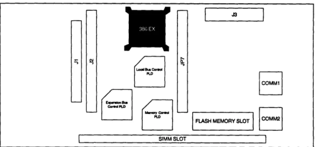
The host processor sections consists of the Intel 386 EX evaluation board from Intel and the 7847 Digital to Analog converter from Analog Devices. The 386 EX evaluation board includes memory, peripheral headers, programmable logic devices, in addition to the 386 EX microprocessor. (See figure 10) An overview of the major components used in the implementation will be given, for a more detailed discussion of the functional units please see the 386 EX hardware reference and the 386 EX evaluation board manual. [13][14]
L~u cm.*d RD C.*dew 0~ I XJ3 BE---___mI
FLASH MEMORY SLOT
I SIMM SLOT I
Figure 10: The 386 EX Board Functional Units
The Evaluation Board
5 .1 MEMORY
There are three different types of memory on the 386 EX Evaluation Board. These include SRAM, DRAM, and flash memory. The system SRAM is 32 Kbytes. The primary purpose use of the SRAM is to support the System Management Mode (See 386 EX Section). The SRAM can be used for other purposes, however care must be taken to ensure that the SRAM does not lie in the address space for the system DRAM. In this implementation neither the System Management Mode nor the SRAM is used.
The DRAM memory occupies slot US4 with a single sided 1 Mbyte SIMM.
Additional Memory can be added by using single sided SIMMs with larger capacity, e.g. a 1 Mbyte x 32 SIMM and 4 Mbyte x 32 SIMM would increase the DRAM memory size to 4 Mbytes and 16 Mbytes respectively. The user must select single sided SIMMs as double sided SIMMs require two additional row address strobes, RAS that the board does not support. Access to the DRAM is provided by two wait states at the 25 MHz Operation.
The Flash memory on the evaluation board consists of the 512 Kbyte Flash 28F400 BX Memory. Access to the device is controlled by two chip selects /UCS and /C6. /UCS is used to access the entire 512 Kbyte array, while /C6 can only access the lower 256 Kbytes of the array. The 28400 BX is operated in a 16 bit wide (word) configuration by
tying its /BYTE line high and tying its address AO input to the 386 EX's Al output. Access to the FLASH is also set for 2 wait states at 25 MHz operation.
5 .1.1 Programming Flash Memory
The Flash 28F400BX has the capability to be in-socket programmed. This means that it can be programmed from the comm port. This capability is provided by programming the 'boot block' section with a program that sets up the serial ports and provides instructions for programming the EPROM. The boot block is a special section of the EPROM that is write protected and cannot be in-socket programmed. The port 1.5 pin (/PRGEN) controls the voltage on the V, pin of the EPROM. When /PRG_EN is active (low) the Voltage on the Vp goes to 12 V. The RAMWE signal which is connected to the write enable pin (/WE) on the EPROM also controls the writing of the EPROM.
The Flash Memory actually consists of seven separately erasable and
programmable blocks, including the 16K write protected boot block. The Command User Interface (CUI) provides the interface between the microprocessor and the internal flash memory. Program commands and be executed by writing to the CUI. In addition to the /WE signal there is also /OE, /CE, and I/BYTE. The /OE signal allows the driving of output signals. The chip enable signal activates the internal logic, decoders, and sense amplifiers. The /BYTE signal indicates whether or not the Flash operates in byte wide mode. On the evaluation board the BYTE signal is wired high indicating that the FLASH is configured for 16 bit wide operation. In addition to these signals the /RP reset/ deep power down signal controls whether or not the any block EPROM can be written to, and it also locks the boot block. On the evaluation board, this signal is wired to +12V
indicating that the boot block is write protected. For more information about the 28F400 Flash memory refer to its data sheet. [15]
5 .2 PERIPHERAL CONNECTORS
The peripheral connectors on the evaluation board include two 32x2 D type connectors, J2 and JP7, and one 20x2 connector, J1. The J1 and J2 connectors are of the PC/104 standard. One of the larger connectors, JP7 is used to allow the connection of the D/A to
Parallel Ports 1 and 3, similarly the other large connector J2, provides the lower byte of the expansion bus and is connected to the Port A and D lines from the 68HC11 (see schematics or figure 5).
5 .3 PC/104 BUS
The PC/104 bus has been designed for embedded applications that allow a high degree of compatibility with existing Industry Standard Architecture (ISA) bus designs. The J1 and J2 connectors have the same logic signals as the ISA architecture present on the PC/AT. The arrangement of the connectors as shown on figure 10 occupies less space and
consumes less power than the AT ISA implementation, and allows the cards to be stacked. This arrangement is geared towards embedded applications where power and space constraints are of concern.
5 .4 PROGRAMMABLE LOGIC DEVICES
The programmable logic devices provide control signals for the EVB and the 386 EX. There are 3 different PLDs. The Local Bus PLD controls the operation of the local bus, generation of the 01 clock signal, and generation of the data and expansion bus enables. The Memory Control PLD generates access signals for the Flash Memory and DRAM, including the /RAM_WE signal which connects to the Flash and the SRAM. The Expansion Bus PLD decodes memory and I/O accesses. It provides the correct strobes for these addresses that correspond to the expansion bus.
5 .5 ASYNCHRONOUS PORTS
There are two serial port connectors present on the 386 EX evaluation board. COM1 is a male DB9 connector that is configured for Data Carrier Equipment (DCE) . It has the RS232 functionality of a modem or serial port with all the status and control signals connected to the processor.
COM2, is a female DB9 connector that is configured for Data Terminal
lines have been swapped to allow communication with the PC or other peripheral device with a serial connection (see below). This port is used for debugging.
PC
COM2
Figure 11 : DB9 with the Rx and Tx connections swapped.
5 .6 386 EX
The 386 EX consists of the 386 SX processing core and several on chip peripheral units that have been added to facilitate the creation of embedded applications. These include: the DMA Unit, Bus interface unit, Chip Select Unit, JTAG test Unit, Clock and Power Management Unit, DRAM Refresh Unit, Watchdog Timer Unit, Serial Communications Unit, Timer Unit, and the Interrupt Control Unit (ICU), as shown below. Design considerations may warrant the use of the Chip-select Unit, the DMA unit, ICU, or the Synchronous Serial I/O Unit (see Section 7). The Asynchronous Serial Unit is also used by the iRMX Operating System, for debugging purposes.
Figure 12: The 386 EX Functional Components
5 .6.1 Parallel Ports
The 386 EX has 3 general purpose I/O ports, consisting of eight pins each. However, most of these I/O pins are multiplexed with other functions such as asynchronous serial I/O. In fact, the asynchronous communications clock, COMCLK is multiplexed with Port
3 pin 7. COMCLOCK connects to the 1.8432 MHz generator and cannot be used for general purpose I/O. In this implementation Port 3 pins 0-6 are used to provide the 7 bits of data for the Analog Devices 7847 Digital to Analog converter (D/A). Port 1 pin 7 provides the MSB of data to the D/A. After the byte of data has been placed on the input pins of the 7847, the data is latched by asserting the write signal. Port 1 pin 6 provides the
write signal for the 7847.
DB3-0 DB10-DB4
D/A
DB11 /WR ' Port3.6-0 , Portl.7 ,_ Port1.6Figure 13: Parallel Port Connection to the D/A
5 .6.2 DMA Unit
The DMA unit has two channels, 0 and 1, which operate independently of each other. Each channel can function in one of several operating modes, and can transfer data of byte or word widths. The bus arbiter is also a part of the DMA unit. It receives requests from the DRAM refresh controller, and the external Bus Master, in addition to the two DMA channels.
The channel consists of three items: the Requester, the Target and the Byte count. These items are identified by the registers that define the memory or I/O device
requesting DMA service (the Requester). The Requester is the only item that can initialize or end a DMA process. The Target (address) is the area of memory with which the requester wishes to exchange data. The Byte count indicates the amount of data to be transferred.
The DMA Unit includes features not found in the 8237 DMA family, however it can be configured to behave in a 8237 like manner.
5 .6.3 Chip Select Unit
The Chip Select Unit can generate up to eight different chip selects. A chip select is configured by assigning a series of addresses to a given chip select. These addresses are the higher order 11 bits of a 26 bit address, the lower 15 bits are masked out. Thus, each chip select is assigned a block of memory. Whenever the selected region of memory is referenced by the 386 EX address lines, the chip select for that region is asserted. This can be used to memory map I/O or other peripheral devices without the need for external glue logic.
The Interrupt Control Unit (ICU) consists of two cascaded 8259A modules. The ICU supports up two 16 interrupt requests (8 internal, 8 external). Interrupt requests are put in the Interrupt Request Register which contains one bit for each interrupt request signal. A corresponding bit is set for each interrupt request. If a conflict exists, the priority resolver chooses which request has the highest priority. The priority resolver controls the interrupt request line to the CPU. Additional interrupt requests can be serviced by the addition of externally cascaded 8259A's. In the original implementation the ICU was configured to service an interrupt initiated by the INT5 signal. However interrupt latency limited signal responses to 8 kHz, without invoking the DSP routine. A polling approach was subsequently chosen to initiate the transfer of data between the 68HC 11 and the 386 EX processor board.
5 .6.5 The Analog Devices 7847
The 7847 is a 12 bit parallel D/A. It consists of two separate D/A's, channel A and B. The D/A has two ways of formatting the results. A digital conversion can have either a bi-polar 2's complement arrangement or the 12 bits of data can represent an unsigned number. Because the nature of the 68HC11 A/D is uni-polar, it has been chosen to operate the D/A in uni-polar mode as shown in figure 14. Also since the AID in the 68HC11 is 8-bit wide the 7847 is in fact used as a 8-bit D/A with the four least significant bits grounded.
15V
Vout
Figure 14: 7847 In Uni-polar Mode
Data can be latched in one of two ways. Either the /WR signal can be held low and a low to high transition on the corresponding Chip Select (/CSA or /CSB) will cause data to be latched. Similarly, the Chip select can be held low and a /WR signal transition from low to high will cause data to be latched, as shown below.
/CSA
/WR
Figure 15: Latch Control Logic for the 7847
In this implementation, the chip selects for A or B are driven low, and a conversion is initiated by transitioning the write signal, /WR. At this time data is then latched, and a conversion is begun. The /WR signal is controlled by Port 1 pin 6 from the 386 EX as shown in figure 13. The bandwidth of the 7847, is 110 kHz. This is significantly higher than the A/D, however there is some latency involved with the 386EX and the separated parallel port interface. However the majority of the time between outputs is spent calculating the filtered output. In lab tests, with the split byte arrangement (the
arrangement where the input data is spread across Ports 1 and 3 of the 386 EX) the signal could be changed at a frequency of 341 kHz. However, this was without the calculation of DSP algorithm, the true bandwidth of the system is much lower.
The V ddand V,,power supplies for the 7847 are +15 V and -15V respectively. For this implementation it was chosen to make Vef -5V since the uni-polar mode of operation makes Vo= <bit9 aue> xV. This gives a signal with a range from 0 to 5V, which also
matches the operation of the 68HC1 l's A/D. [16]
The system software for the 68HC 11 performs register initialization functions. These functions include initializing the port I/O registers, and configuring the A/D on the 68HC11. These initialization functions are coded directly in Forth and subsequently interpreted by the resident Forth interpreter. The 68HC 11 software must also read the samples from the A/D and send them to the parallel ports. However, because the timing of the section is critical, this software is coded in 68HC11 assembler.
The system software for the 386 performs two functions. The first of which will be to set up the necessary registers for the polling algorithm, and the I/O pins. The second function of the software will be to execute a Digital Signal Processing (DSP) algorithm. Both of these functions are programmed in C, with in-line assembler where necessary.
The DSP algorithm used to test the development system consists of three separate filters. After the A/D converter maps the signal to the discrete-time domain, the signal is filtered using one of three filters. The three filters consist of low, mid-band, and high pass filters. These originally consisted of 33-point finite impulse response (FIR) filters. The original low pass filter was the same filter used in the 6.115 class and the other filters were
designed using Matlab. However, the processing time associated with the 33 point FIR filter was found to be to large and the filter size we first reduced to 27 points and subsequently to 13 points. The three (FIR) filters were then redesigned using Matlab.
6 .1 68HC11 ROUTINES
The 68HC11 from New Micros, contains the MaxForth Kernel in its ROM memory. The MaxForth kernel contains an interpreter to allow Forth commands to be typed in
interactively or downloaded through the PC communications program. The Forth
interpreter resident in the 68HC 11 kernel is adequate for tasks which are not time critical, so the register initialization is written directly in Forth code.
Forth was created in the early '70s by Charles Moore after he became frustrated with conventional languages inability to allow control over a computer system that executed some real time task4.
The Forth language differs from most languages in that it contains elements from both compilation and interpretation. Forth also combines elements from assembly and high level language. Forth differs from other languages in that its functions ('words') are defined based on definitions of other words. This is opposed to constructing new functions by simply listing other functions. Also Forth is a stack based language. Parameters passed to words are explicitly placed on the stack, in what has come to be known as post fix or reverse polish notation. Definitions can be in terms of other words or as we will see later, machine code. When defined in terms of other words these words in turn must be looked up to find the machine code that corresponds to that word. Forth jumps from one word definition to the next since the word definition consists essentially of the addresses of other words. [17] [18] [19]
When Max-Forth interacts with the terminal it operates in interpretive mode. The definitions of words can be interactively entered into the interpreter. However, after the definition of these words has been entered into the dictionary, the words can be
subsequently used without the need to retype the definition.
The Forth programs written for this system perform two actions. First the
programs perform register initializations and then they also collect data from the A/D and subsequently send this data across the Ports to the 386 EX.
The Forth register initialization code does four things. It sets Ports A and D to transfer the byte of data from the A/D, and it powers up and configures the A/D. The initial block of registers sits at Ox1000, however the Max-Forth kernel remaps these
addresses to the OxB000 offset. The initialization of the registers uses the C !, command. This command is a byte write to memory. The user first puts the byte value on the stack then puts the address to which the byte is to be written on the stack and then the user issues the C! command. For example, the following code selects single, continuous mode and channel AN1 for A/D operation:
21 B030 C!
The A/D control register, ADCTL is located at address OxBO30 in the 68HC 11 memory map. The Hex value of 0x21, indicates that bit positions 5 and 1 should be set. When bit
This task incidentally was the control of Radio Telescopes
position 5 is set continuous mode is selected. The lower nibble value of 1 indicates that first channel should be used for conversion. Other register initializations use the same C ! word command.
88 B026 C! ( Set Bits 7 and 3 to outputs) FF B009 C! ( Set Port D 0-7 for outputs)
21 B030 C! ( Continuous, single channel set AN1) 80 B039 C! ( Turn on A/D use external clock)
Example 1: 68HC1 Register Initialization
For a more detailed discussion of the registers involved please refer to the Appendix section.
The performances requirements of A/D control routine necessitate that the routine be coded in 68HC11 assembler. The ADR1 register must be successively read to obtain the successive A/D values when running in continuous mode. Unfortunately, there is no way to know when one register contains valid data and when the next register is being filled. So the approach used is to get the data out of the first register and then wait until 64 cycles later to again get data out of the first register. This increases the sampling period by a factor of 4 from 16 gs to 64 js, thus the maximum allowable input frequency is now 1.= 7.8125 kHz. It is desirable to obtain frequency samples at a rate that would correspond to the A/D bandwidth, however that rate at which samples appear on the port output lines has to be slow enough to allow the 386 EX to calculate the filtered response. In the original implementation, the four registers were read successively. However, because of the number of instructions in the acquisition loop exceeded thirty two, after several samples had been collected the acquisition routine would fall behind the A/D and the next sample read would actually reflect the incorrect sample. For example, suppose that when the A/D was on sample 10 and the acquisition routine was 4 samples behind the A/D, at sample 6. After a while, when the A/D is on sample 17 and the acquisition routine may be on sample 12. Thus the distance between the A/D has changed. If this happens three more times the values output from the acquisition routine will no longer represent sequential samples as the A/D has overlapped the acquisition routine and overwritten the next sample in the sequence.
In order to read these values at 128 clock intervals it is necessary to use 68HC11 assembler. Unfortunately, the Max-Forth kernel does not have an in-line assembler as do
other popular implementations of Forth. For example consider the two following code segments: CODE-SUB GA2D LDX #$B030 LABEL: LDAA $01,X STAA $B000 TAB ANDB $OF LSLB LSLB STAB $B008 INCX XGDX ANDB $F3 XGDX BRA LABEL RTS END-CODE CODE-SUB GA2D CE C, B030 #$B030) A6 C, 01 C, LABEL:LDAA $01 B7 C, B000 , $B000) 16 C, C4 C, $OF) 58 C, 58 C, F7 C,
$B008)
08 C,
8F C, C4 C, $F3) 8F C,20 C,
LABEL) 39 C, END-CODE OF C,8008
F3 C, EC C,Example 2: A Forth word definition a) with a built in assembler b) without an assembler
With Max-Forth code the user must explicitly specify the op-codes involved with the assembler routine, as shown in Example 2B. In the original implementation the code appeared as above, however when the need for a down sampled A/D arouse the code had to be modified with a more time consuming acquisition loop. The current configuration pads the loop with store instructions.5
6 .2 386 EX REGISTER INITIALIZATION
In order to use the functional units on the 386 EX processor it is necessary to write to registers that initialize and configure the units. The first step in accomplishing this is to
5 The STAA (store accumulator A) instruction was chosen as opposed to the standard NOP
because it consumes more time (4 clocks as opposed to 2 for the NOP) , thus there are less instructions to be added. Less instructions added reduces the likelihood of making errors. See the code listings in the Appendix ( LDX ( ,X)
(
STAA (TAB) ( ANDB LSLB) LSLB) STAB INCX) XGDX) ANDB (XGDX) ( BRA RTS)enable the expanded I/O in the memory space. The expanded memory space contains all of the registers necessary for utilization of the parallel ports, interrupt control unit, and the DMA unit. In order to enable the expanded I/O space, the following assembly code is necessary :
mov ax, 8000h /* This will be REMAPCONFIG */ xchg al, ah
out 23h, al /* high byte to 23h */ xchg al, ah
out 22h, al /* low byte to 22h */ out 22h, ax /* Word to 22h */
Example 3: Enabling the Expanded I/O Addresses
The REMAPCONFIG register controls the access to the expanded I/O space. (See Appendix) Most of the code for the initialization of the registers was written in assembler by using the following series of commands:
mov dx, <Port Address> mov ax, <Port, value>
out ax, dx// Places the Word value contained in ax at
<Port Address>
The values can also be read out of the registers with the following instructions: mov dx, <Port Address>
in ax,dx // ax now contains the value at <Port Address>
The first unit that we must set up is the parallel ports. In order to set up the parallel ports it is necessary to write to three registers, PxLTC, PxDIR, PxCFG, where x is a number from 1 to 3 indicating the port number. The PxCFG register controls whether or not the Port is controlled by an internal peripheral or configured for I/O mode and subsequently controlled by the PxLTC and PxDIR registers. The PxDIR register selects whether each pin on the port is an output or a high-impedance input. The PxLTC, data latch register
controls the values driven to the pin. If the pin has been configured as an output, writing a one or a zero to the corresponding bit in the register changes the value on the pin
accordingly.
In this implementation Port 3, pins 0-6 were selected as outputs. The author would have like to use pin 7 as well, however on the Evaluation Board pin 7 is connected to the COMCLOCK which is used for asynchronous communications, therefore it cannot be used for bi-directional I/O. Port 1 pins 6 and 7 were also used as outputs, and Port 2
pin 1 was used as an input. Pin 7 was used to drive the most significant data bit on the D/A. Pin 6 was used to drive the /WR line of the D/A. Because of the unavailability, of Port 3 pin 7, it is necessary to distribute the byte of information calculated by the DSP routine across Port 3 and Port 1. Also care must be taken to ensure that the Port 1 pin 6 bit does not get written at inopportune times because it controls the start of a conversion of the D/A. In order to accomplish this spread of the byte, the byte is written to the Port 3's data register, P3LTC, unaltered. Then the signal byte is ANDed with 0x80 and subsequently written to the P1LTC data register. This masks out the least significant 6 bits allowing the most significant bit of data to pass through. It also sends the Port 1, pin 6 bit low. The reader will recall that D/A conversion is begun on a low to high transition, thus it is necessary to have the /WR signal low before a conversion can be initiated. One would have to be cautious about transitioning the write signal and the most significant bit at the same time, however in lab tests the correct values were written to the D/A. This is due to the fact that the actual write of data occurs during the low to high transition of the /WR signal. The write is accomplished by sending the Port 1 pin 6 write signal high by ORing the value 0x40 with the value currently contained in the Port 1 data register. The OR is necessary because the value on the DB 11 (Port 1 pin 7) should not change when the /WR signals transitions to the high value. This process continues as other bytes are
written.
6 .3 THE DSP ALGORITHMS
The DSP algorithm used to test the development system consists of three separate filters. The A/D converter can map the signal to the discrete-time domain, with a sampling frequency of 62.5 kHz. By the Nyquist criterion, input signals up to 31.25 kHz can be successfully converted without aliasing. However, the calculation of the DSP algorithm takes processing time, this processing time limits the rate at which data can be presented to the 386 EX. Originally, it was thought that the 386 EX could compute the convolution in the 16 ýts sample time. However experimentation revealed that the original C algorithm (See eval.c in the code listings) took 390 gs to compute an output. The C algorithm was abandoned and the routine coded in assembler and the size of the filter reduced to 27
points, this reduced the output calculation latency to 120 gs. It was then decided to further reduce the filter size to 13 points so that the latency time would be -60 gs, which would correspond to the 64 gs reduced sampling period of the 68HC 11. This resulted in a maximum input frequency of 7.8125 kHz.
The signal is filtered using one of three filters. The three filters consist of a low, band, and high pass filters. These are 13-point finite impulse response filters. The discrete time frequency responses are shown in figures 16 a-c, the cor responding continuous time domain frequency responses are shown in figure 17 a-c.
Redesigned (firl) Low Pass Filter Frequency Response
The original (firl) Mid-Band Filter Freq Responses
0.1 0.2 0.3 0.4 0.5 0.8 0.7 0.8 0.9
Figure 16 a-c Discrete Time Frequency Responses
0.1 0.2 0.3 0.4 0.5 0.6 0.7 0.5 0.9
The original (fir) High Pass Filter Freq Responses
v
1 · · · --· ·