The Design of a Deep Space Transponder Regenerative
Ranging Unit
by
David Samuel Warren
Submitted to the
Department of Electrical Engineering and
in partial fulfillment of the requirements
Computer Science
for the degree of
Master of Science
at the
MASSACHUSETTS INSTITUTE OF TECHNOLOGY
June, 1995
David Samuel Warren, 1995. All rights reserved.
The author hereby grants to MIT, Jet Propulsion Laboratory, NASA,
and Caltech permission to reproduce and to distribute publicly paper
and electro i copies of this/4esis document in whole or in part.
Author ...
..
Department of Electrical Engineering and Computer Science, May 26, 1995
Certified by ...:.
, ...
James K. Roberge, Prof. of Elec. Eng., Thesis Supervisor (Academic)Certified
by
......
Arthur W. Kermo Company Supervisor (Jet Propulsion Laboratory)
Accepted by
... Ins . .. . l - .. . - -. ....
. . . .~~~~~~~~~~~~~~~~~~~~~...F. R. Morgenhaler, Chair, artment Committee on Graduate Students
MASACHUSET'ITS INSTITUTE
The Design of a Deep Space Transponder Regenerative Ranging Unit
by
David Samuel Warren
Submitted to the Department of Electrical Engineering and Com-puter Science on May 26, 1995, in partial fulfillment of the
require-ments for the degree of Master of Science
Abstract
Ranging signals are transmitted from the ground to deep space spacecraft, then returned to the ground in order to determine the spacecraft's distance from the earth. Currently, the transponders used on these spacecraft have no capability to regenerate the ranging signals. A scheme for implementing this regeneration, which leads to a dramatic reduction in the ranging signal's noise power (up to 40 dB) is proposed. The regeneration system was
designed, and implemented with Actel field programmable gate arrays (FPGAs). After several iterations, the design was simulated successfully.
Thesis Supervisor: Professor James Roberge Title: Professor of Electrical Engineering
Acknowledgments
The author gratefully acknowledges the assistance of several people. Arthur Kermode and Prof. J. K. Roberge supervised this work, and made this project possible. John Smith and Glenn Johnson provided crucial information on the sequential and PN ranging systems, as well as providing suggestions on how they could be modified. Renee Watson and Dr. Sela-hattin Kayalar provided assistance with Comdisco SPW, and made many suggestions involving design improvements. Todd Mackett provided the adapter needed to program the Actel FPGAs. Jeff Wong and Prof. V. M. Bove allowed the use of facilities at the MIT Media Laboratory to complete some of the hardware construction.
Table of Contents
Chapter 1. Introduction...15 1.1 General Overview ... 15 1.2 Satellite Communication ... 15 1.3 Why regenerate? ... 16 1.4 My Thesis Project ... 16Chapter 2. Theoretical Analysis ... 19
2.1 Ranging ... .19 2.1.1 Sequential Ranging ... 19 2.1.2 PN Ranging ... 20 Chapter 3. Design ... 25 3.1 Overview ... 25 3.2 Comdisco Designs ... 25 3.2.1 Generation Unit ... 25 3.2.2 Regeneration Unit ... 26
3.3 Mentor Graphics Designs ... 28
3.3.1 Generation Unit ... 28
3.3.2 Regeneration Unit ... 28
3.4 Actel FPGA Design ... 29
3.5 Physical Hardware Construction ...29
Chapter 4. Results and Discussion ... 33
4.1 Comdisco Simulation Results ... 33
4.2 Mentor Graphics Simulation Results ... 34
4.3 Post-layout Timing Simulation Results ... 37
Chapter 5. Conclusion ... 41
5.1 Summary ... 41
5.2 Recommendations ...41
Appendix A. Graphs of PN component Auto- and Cross-correlation functions ... 43
A.1 Graphs of Autocorrelation Functions ... 43
A.2 Graphs of Cross-correlation Functions ... 47
Appendix B. Comdisco Block Diagrams ... 55
Appendix C. Systems used to Test Comdisco Designs ... 171
Appendix D. FSM description files ... 205
D.1 FSM State Diagram ... 205
D.2 Fsmc input file ... 206
D.3 FSM state file ... 207
D.4 FSM equation file ... 210
Appendix E. Mentor Graphics Schematics ... 211
Appendix F. Nonstandard Actel Macros ... 257
List of Figures
Figure 2.1: Spectrum of combined PN sequence ... 21
Figure 2.2: FFT of clock component ... 22
Figure 2.3: Clock component and combined PN sequence (time domain) ...22
Figure 3.1: Simplified Block Diagram of Regeneration Unit (with transponder) ...26
Figure 3.2: Generation Unit Wirewrap Board Schematic ... 30
Figure 3.3: Regeneration Unit Wirewrap Board Schematic ... 31
Figure 4.1: Comdisco simulation output - no noise on input ...33
Figure 4.2: Comdisco simulation output - additive white noise on input ... 34
Figure 4.3: Mentor functional simulation without additive noise ...35
Figure 4.4: Mentor functional simulation with additive noise ... 36
Figure 4.5: Mentor timing simulation - Clock speed too high ... 38
Figure 4.6: Mentor timing simulation - Clock speed slow enough ...39
Figure A. 1: Graph of Autocorrelation Function for Length 2 PN component ... 43
Figure A.2: Graph of Autocorrelation Function for Length 7 PN component ... 44
Figure A.3: Graph of Autocorrelation Function for Length 11 PN component ... 44
Figure A.4: Graph of Autocorrelation Function for Length 15 PN component ... 45
Figure A.5: Graph of Autocorrelation Function for Length 19 PN component ... 45
Figure A.6: Graph of Autocorrelation Function for Length 23 PN component ... 46
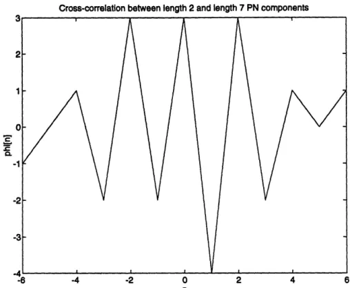
Figure A.7: Graph of Cross-correlation Function for Length 2 and 7 PN Components ... 47
Figure A.8: Graph of Cross-correlation Function for Length 2 and 11 PN Components ... 47
Figure A.9: Graph of Cross-correlation Function for Length 2 and 15 PN Components ... 48
Figure A. 10: Graph of Cross-correlation Function for Length 2 and 19 PN Components ... 48
Figure A. 11: Graph of Cross-correlation Function for Length 2 and 23 PN Components ... 49
Figure A. 12: Graph of Cross-correlation Function for Length 7 and 11 PN Components ... 49
Figure A. 13: Graph of Cross-correlation Function for Length 7 and 15 PN Components ... 50
Figure A.14: Graph of Cross-correlation Function for Length 7 and 19 PN Components ... 50
Figure A. 15: Graph of Cross-correlation Function for Length 7 and 23 PN Components ... 51
Figure A. 16: Graph of Cross-correlation Function for Length 11 and 15 PN Components ... 51
Figure A.17: Graph of Cross-correlation Function for Length 11 and 19 PN Components ... 52
Figure A. 18: Graph of Cross-correlation Function for Length 11 and 23 PN Components ... 52
Figure A. 19: Graph of Cross-correlation Function for Length 15 and 19 PN Components ... 53
Figure A.20: Graph of Cross-correlation Function for Length 15 and 23 PN Components ... 53
Figure A.21: Graph of Cross-correlation Function for Length 19 and 23 PN Components ... 54
Figure B.1: 2code_combiner block diagram ... 57
Figure B.2: clockacq block diagram ... 59
Figure B.3: code_combiner block diagram ... 61
Figure B.4: code_convert block diagram ... 63
Figure B.5: comp_rec_all block diagram ... 65
Figure B.6: comp_rec_wctl block diagram ... 67
Figure B.7: comp_recover block diagram ... 69
Figure B.8: control_cnt block diagram ... 71
Figure B.9: control_fsm block diagram ... 73
Figure B. 19: nodly block symbol ... 97
Figure B.20: nodly block parameters ... 97
Figure B.21: phase_error block diagram ... 105
Figure B.22: pn_2comp block diagram ... 107
Figure B.23: pncompcount block diagram ... 109
Figure B.24: pndelays block diagram ... 111
Figure B .25:png en2 block diagram ... 113
Figure B.26: pn.generator block diagram ... 115
Figure B.27: pnregen block diagram ... 117
Figure B.28: pnsource block diagram ... 119
Figure B.29: pnsource2 block diagram ... 121
Figure B.30: regenranging block diagram ... 123
Figure B.31: regen_reset block diagram ... 125
Figure B.32: rsum block diagram ... 127
Figure B.33: single_pn block diagram ... 129
Figure B.34: singlepn2 block diagram ... 131
Figure B.35: vec2int block symbol ... ... 133
Figure B.36: vec2int block parameters ... 133
Figure B.37: veclogic block symbol ... 141
Figure B.38: veclogic block parameters ... 141
Figure B.39: vec_rotate block symbol ... 151
Figure B.40: vec_rotate block parameters ... 151
Figure B.41: vecscalogic block symbol ... 159
Figure B.42: vec_sca_logic block parameters ... 159
Figure B.43: xnor block diagram ... 169
Figure C.1: 2comp.rectest block diagram ... 173
Figure C.2: acqtest.detail block diagram ... 175
Figure C.3: acqtest.system block diagram ... 176
Figure C.4: cmpcnttest block diagram ... 178
Figure C.5: combiner_test block diagram ... 180
Figure C.6: comprectest block diagram ... 182
Figure C.7: comprec.test2 block diagram ... 184
Figure C.8: comprectest3 block diagram ... 186
Figure C.9: count_test block diagram ... 188
Figure C.10: fsm_test block diagram ... 190
Figure C. 11: int2vec_test block diagram ... 192
Figure C.12: local_pn_test block diagram ... 194
Figure C. 14: rangingtest block diagram ... 198
Figure C.15: single_test block diagram ... 200
Figure C. 16: vec_logicjtest block diagram ... 202
Figure C.17: vec_rot_test block diagram ... 204
Figure D. 1: State Diagram of Control FSM ... 205
Figure E. 1: 7cnt schematic ... 213
Figure E.2:1 lcnt schematic ... 213
Figure E.3: 5cnt schem atic ... 213
Figure E.4: l9cnt schematic ... 214
Figure E.5: 23cnt schematic ... 214
Figure E.6: 7code schematic ... 216
Figure E.7:1 lcode schem atic ... 216
Figure E.8: l5code schem atic ... 217
Figure E.9: 9code schematic ... 217
Figure E. 10: 23code schematic ... 218
Figure E. 11: 7decode schematic ... 220
Figure E. 12:1 ldecode schematic ... 220
Figure E. 13: 15decode schem atic ... ...220
Figure E.14: 9decode schem atic ... 221
Figure E.15: 23decode schematic ... 221
Figure E. 16: 7gen schematic ... 223
Figure E. 17:1 lgen schem atic ... 223
Figure E.18: 5gen schematic ... 224
Figure E.20: 23gen schematic ... 224
Figure E. 19: 9gen schem atic ... 225
Figure E.21: 7rec schematic ... 227
Figure E.22: 1 rec schematic ... 227
Figure E.23: 15rec schematic ... 228
Figure E.24: 19rec schematic ... 228
Figure E.25: 23rec schematic ... 229
Figure E.26: 7reverse schematic ... 231
Figure E.27:1 lreverse schem atic ... 231
Figure E.28: 5reverse schematic ... 232
Figure E.29: l5reverse schematic ... 232
Figure E.30: 23reverse schematic ... 233
Figure E.31: 32cnt schematic ... 235
Figure E.32: andl6 schematic ... 237
Figure E.33: cmpl6 schematic ... 239
Figure E.34: combiner schematic ... 241
Figure E.35: control schematic ... 243
Figure E.36: generate schematic ... 245
Figure E.37: maxcount schematic ... 247
Figure E.38: negacc schem atic ... 249
Figure E.39: regl6 schematic ... 251
Figure E.40: regenerate schem atic ... 253
Figure F.9:tt02 schem atic ... 268
Figure F. 10: ttlO4 schematic ... 268
Figure F. 1: ttl08 schem atic ... ... 268
Figure F.12: ttl schem atic ... 269
Figure F.13: ttll 1 schematic ... 269
Figure F.14:ttl20 schem atic ... 269
Figure F. 15:ttl21 schem atic ... 270
Figure F.16:ttl32 schem atic ... 270
Figure F.17:ttl38 schem atic ... 270
Figure F.18:ttl161 schematic ... 271
Figure F. 9:ttl169 schem atic ... 271
Figure F.20:ttl 94 schem atic ... 272
Figure F.21: ttl377 schem atic ... 272
Figure F.22:ttl175 schem atic ... 274
Figure F.23:ttl244 schem atic ... 276
Figure F.24:ttl257 schem atic ... 278
Figure F.25:ttl283 schem atic ... 280
Figure G.1: 1 lm ux_l schem atic ... 281
Figure G .2: lm ux_2 schem atic ... 282
Figure G .3: 1 lrec_l schem atic ... 283
Figure G.4:1 lrec_2 schem atic ... 284
Figure G.5: 15m ux_l schem atic ... 285
Figure G .6: 15m ux_2 schem atic ... 286
Figure G.7: 15rec_l schem atic ... 287
Figure G .8: 15rec_2 schem atic ... 288
Figure G.9: generate2 schematic ... 289
Figure G .10: regenl schem atic ... 290
Figure G. 11: regen2 schematic ... 291
Figure G.12: regen3 schematic ... 292
Figure G.13: regen4 schematic ... 293
Figure G.14: regen5 schem atic ... 294
List of Tables
Table 2.1: Component codes for JPL PN ranging system ... 20
Chapter 1
Introduction
1.1 General Overview
For many deep space missions, the location of a spacecraft must be known precisely, so that its trajectory can be determined and/or corrected. This location can be determined from a combination of ranging data and doppler data. The doppler data allows operators to determine in which direction the spacecraft is located, as well as in which direction it is moving. The ranging data allows a determination of the distance between the spacecraft and the earth to be made.
The ranging data is collected by sending ranging signals to the spacecraft, phase mod-ulated onto a carrier signal. The signals are returned to the earth through the spacecraft transponder, and the ground station is able to determine the time delay caused by the dis-tance the signal travels. This time delay, called the round trip light time (RTLT), can be used to calculate the spacecraft's distance from the earth. Using the current system for ranging, this distance can be measured to within approximately 10 meters.
1.2 Satellite Communication
There are three types of signals sent between the spacecraft and the ground station. Com-mand signals are sent from the ground to the spacecraft, and are the means by which oper-ators on the ground control the spacecraft. These signals include instructions, such as "turn on thruster number three for 0.14 seconds", "power up the imaging system in camera number four", or "start sending recorded data now".
Telemetry signals are sent from the spacecraft to the ground, and are the means by which scientific data, and spacecraft status data is returned to the operators. These signals include data, such as "thruster six fired successfully", "imaging system is on", or scientific data from an onboard instrument.
Ranging signals are sent both from the ground to the spacecraft, and from the space-craft to the ground. As explained above, these signals are used to determine the exact loca-tion of the spacecraft. These ranging signals are the focus of the remainder of this paper.
system to be maintained, these signals must be generated either in-phase with the received ranging signals, or differing from them by only a constant phase shift.
By regenerating the ranging signals onboard the spacecraft, it is possible to dramati-cally improve the signal-to-noise ratio (SNR) of the retransmitted signal. This improve-ment, in turn, allows the original ranging signals to be transmitted with less power, even though the confidence in their measurement accuracy remains the same. By using less power for ranging, there is more power available for command and telemetry, which allows these signals to use higher data rates, reducing the amount of antenna time required for a given transmission. Since antenna time is a scarce resource, this reduction will bene-fit most deep space missions.
1.4 My Thesis Project
I have designed a regenerative ranging system, based on pseudonoise (PN) ranging (the different types of ranging are described in Section 2.1). It provides a significant improve-ment in the ranging SNR, at the expense of some added complexity onboard the space-craft. The SNR improvement is realized mainly through reducing the noise bandwidth of the ranging signals. In the turn-around ranging system, the ranging signals are amplified via a band-pass amplifier with a bandwidth of approximately 1.5 MHz. These signals, then, have a noise bandwidth of 1.5 MHz. In the regenerative system, the noise bandwidth is reduced to the loop bandwidth of a phase-locked loop at the input of the system. This loop bandwidth is approximately 100 - 200 Hz. This difference causes a theoretical reduc-tion by a factor of approximately 104, or 40 dB, in the noise power. The actual improve-ment in ranging SNR approaches this number.
In the next several chapters, some of the theory behind the ranging systems, a detailed account of the design methods employed, and some results and conclusions will be
Chapter 2
Theoretical Analysis
2.1 Ranging
Currently, there are two main systems that perform ranging: sequential ranging, and pseudonoise (PN) ranging. The transponder used for deep space missions, and the ground stations that are part of the Deep Space Network (DSN), currently use sequential ranging. 2.1.1 Sequential Ranging
In the sequential ranging system [1], [5], [8], the ranging signal consists of a sequence of square waves with successively doubling periods, each called a component. The amount of time for which each component is transmitted is determined from mission requirements, and can vary over the lifetime of a mission. The main factor affecting these transmission durations is the integration time required in the ground station. The integra-tion time, in turn, is affected by the signal-to-noise ratio of the signal received on the ground. The lower the signal-to-noise ratio falls, the longer the integration time must become. Currently, the options for increasing the signal-to-noise ratio for this ranging sys-tem are difficult to implement and/or otherwise undesirable.
The accuracy of the system is determined by the highest frequency component sent to the spacecraft. Since the phase of the returned signal is measured to about 1 part in 100, the accuracy of the system is approximately 1/100 of the wavelength of the highest fre-quency component [7].
The system also introduces an ambiguity with a period equal to that of the lowest fre-quency component. This ambiguity is created since the only measurements that are taken are the phases of each component. Since these phases will all be the same when the space-craft is at distance of , as they will be when the spacespace-craft is at distance of C plus any
integer multiple of the wavelength of the lowest frequency component, there is ambiguity in the measurement. To eliminate this ambiguity, it is necessary to know, a priori, where the spacecraft is located, to within one wavelength of the lowest frequency component. This estimate can be made by either forcing the above wavelength to be larger than the distance the spacecraft will travel from the earth, or through using principles of celestial
dom stream of bits. This bit stream is chosen such that it will have a sharp peak in its auto-correlation function. In addition, to increase the speed at which the PN code can be acquired, the bit stream is composed of several shorter sequences (or components) that are combined using boolean logic. These components are chosen to minimize their respective cross-correlations. In this fashion, the phase of each component can be accurately deter-mined by correlating the component with the entire combined sequence.
To allow for minimized cross-correlations, the component lengths must all be rela-tively prime. In addition, to facilitate easy acquisition, one component typically has length two, and is called the clock component. The remaining component sequences are chosen such that on average they maintain high and low logic levels for approximately equal amounts of time. The actual components chosen by the ranging group at JPL are shown in Table 2.1. Graphs of their auto- and cross-correlation functions are shown in
Table 2.1: Component codes for JPL PN ranging system. Figures A.1 - A.21, in Appendix A.
These components are combined into a single PN sequence through a simple boolean function, shown in Equation (2.1).
Component Length Component Sequence
2 (clock) 10 7 1110100 '11 11100010110 15 111100010011010 19 1111010100001101100 23 1111010110011001010000 23 111111010110011001010000
PN - F(Cj) = C2 (C7+ C11+ C5 + C1 9+ C23) + (C7 C C15 * C9 C2 3) (2.1) Where Cn represents the PN component of length n, represents logical AND, and
+ represents logical OR.
This combination results in a 6.25% reduction in the power of the clock signal. This power is spread into sidebands around the frequency of the clock component, producing the spectrum shown in Figure 2.1. The spectrum of the pure clock component is shown in
·,~ ~ Frequency Spectrum of Combined PN Sequence
10o lO' lo' 102 1010'0 10 Frequency x 106
Figure 2.1: Spectrum of combined PN sequence.
Figure 2.2, for reference. In the time domain, the combined PN sequence appears very similar to the clock component, except that the combined sequence is missing a few pulses. In other words, the combined sequence will alternate between 1 and 0, except that there will be a few instances of three l's in a row, or three 0's in a row. Both the clock component and the combined sequence are shown in the time domain, in Figure 2.3.
The accuracy of the PN system is comparable to that of the sequential system, since both systems depend on the highest frequency present (the clock component, in the case of the PN system) for taking their most accurate measurement. Both systems allow the use of up to 2 MHz clock components. The sequential system, however, currently uses only a
-in-1
0 1 2 3 4
Frequency
5 6 7 8
xlo" Figure 2.2: FFT of clock component.
Clock component of PN sequence
0 200 400 600 800 1000 1200 1400 1600 1800 2000
n
Combined PN sequence
n
Figure 2.3: Clock component and combined PN sequence (time domain).
100
y1
MON
i .i i
1 MHz clock component. Similar to the case of the sequential system, it is also possible for there to be ambiguity in the range measurement. In the PN system, however, this ambi-guity results from the finite length of the PN sequence. The ambiambi-guity in the measurement becomes the distance an EM wave travels in one cycle of the combined PN sequence.
Chapter 3
Design
3.1 Overview
The regenerative ranging system was designed as two separate units. One unit generates a PN ranging code, for testing purposes; the other performs the actual regeneration.
Both units were initially designed in Comdisco SPW (a signal processing CAD sys-tem), in order to develop functional algorithms. The units were developed concurrently, as there is a great deal of overlap in the Comdisco blocks used. Once the algorithm develop-ment was completed, the units were impledevelop-mented in hardware using Mentor Graphics Design Architect, a schematic capture tool. After thorough simulation, the designs were laid out into Actel field programmable gate arrays (FPGAs) using the Actel Designer Advantage software. The FPGAs were then programmed, and wired onto a prototype cir-cuit board for testing.
3.2 Comdisco Designs
The following sections (3.2.1 and 3.2.2) will explain only the general design of the gener-ation and regenergener-ation units. For a detailed description of the inputs, outputs, and function of each non-primitive Comdisco block used, as well as a copy of their lower-level block diagrams, see Appendix B. For a similar description of the systems used to test several of the Comdisco blocks, see Appendix C.
3.2.1 Generation Unit
The generation unit (shown in Appendix B as the pn_source2 block, on Pages 120-121) is comprised of two main sections: The component generators, and the component combiner. The component generators are shift registers of length equal to the length of the component that they generate. They have load inputs that enable the bit sequences of a component to be initialized, and have both parallel and serial outputs. This design allows the blocks to be reused in the regeneration unit.
The component combiner implements a simple boolean function (Equation (2.1), in Section 2.1.2) that combines the 5 components and the clock into a single PN sequence.
Pages 122-123) consists of a clock recovery system, five independent component recovery systems, five matching component generators, and a component combiner circuit. A sim-plified block diagram of the system is shown in Figure 3.1.
f
rangingcarrier
ranging out in _ |_ n recovered codes WVaonvalUDA clockFigure 3.1: Simplified Block Diagram of Regeneration Unit (with transponder). The clock recovery system (shown in Appendix B as the clock_acq block, on Pages 58-59) is implemented as a phase-domain model of a phase-locked loop. It consists of a phase error detector, a loop filter, and a signal generator. The phase error detector measures phase error by integrating the difference between an advanced version of the clock, and a delayed version of the clock, each multiplied by the incoming PN sequence. The integration is performed over one half the period of the clock. Since it is difficult to generate an advanced version of the clock, the comparison is actually performed on the clock, and a version of the clock that is delayed by 2AT. The recovered clock then becomes the original clock, delayed by AT.
Transponder
Recovery
Clock
Code
Combiner
Code
Component
Recovery
4i Do -T - _ . _____ _~~~~~~ ! ISince the phase error detector performs an integration, its output is only valid at a lower sampling rate than its input. This difference in rates requires that the portion of the loop between the phase error detector and the repeat block run at a lower sampling rate than the rest of the system. This system is called a multirate simulation in Comdisco, and it requires careful handling of simulation parameters to insure correct output.
When scaling factors due to the sampling rate, and the method by which integrators are implemented in Comdisco are taken into account, the effective loop transmission has the form shown in Equation (3.1). This transfer function has a crossover frequency of
co = 89.6r a d, and a phase margin of 90.0'. It allows the loop to track step changes, as well
S
as linear ramps, of the phase of the input clock, with zero error.
H(s) = 8.96x 10- 2 (1000s + (31)
2 S
The five component recovery systems are all identical, except for their bit-width, and all five operate independently. Each recovery system consists of a local component gener-ator, several correlators, logic to find the peak of the correlations, several registers, and control logic. The system computes the correlation between all possible phases of the locally generated component and the PN sequence that is input to the unit. It then finds the peak value of these correlations, and adjusts the phase of the local component so that this peak will correspond to a phase offset of zero.
The phase of the component generator in each component recovery system is then loaded into one of the five stand-alone component generators in the regeneration unit. These generators are the same as the ones used in the generation unit. The outputs of these generators are then fed into the component combiner circuit, which is identical to the com-biner circuit in the generation unit. The output of the comcom-biner circuit is the regenerated PN sequence that the system outputs.
A finite state machine (FSM) was designed to control the data paths that perform these functions, using the FSM design tools also used in 6.111 (Digital Systems Laboratory). The fsmc input file, and the equation and state output files are shown in Appendix D. A
3.3.1 Generation Unit
The generation unit (shown in Appendix E as the generate schematic, on pages 244-245) consists of five component generators, a component combiner, and an 8-bit adder. The component generators, as in the Comdisco design, are simply circular shift registers, sequentially outputting a component code that is input with a parallel load. Again, the component generator is a boolean logic function, obeying Equation (2.1), as stated above in Section 2.1.2. The output of the component generator then controls a multiplexor, let-ting the noiseless PN sequence take on an 8-bit value of either 96, or -96. An 8-bit noise input is then added to this value. The resulting quantity, after passing through an 8-bit D/A converter becomes the output.
3.3.2 Regeneration Unit
The regeneration unit (shown in Appendix E as the regenerate schematic, on pages 252-253) consists of five component recovery systems, five matching component generators, and a component combiner. The component generators and component com-biner operate identically to those described above, for the generation unit (as shift regis-ters, and a boolean function, respectively).
The regeneration unit takes its input as an 8-bit value that is the output of an A/D con-verter. The sampling rate on the A/D converter is set to four times the frequency of the clock component of the PN sequence. It is worth noting that the Mentor Graphics design of the regeneration unit does not contain a clock recovery circuit. This omission is pur-poseful, and is due to the fact that the clock recovery circuit is assumed to be implemented as an analog phase-lock loop before the A/D conversion takes place. In addition, this phase-lock loop outputs the sampling clock for the A/D converter (at four times the fre-quency of the PN clock component).
Each component recovery system consists of a local component generator, a set of cor-relators, and logic to find the peak of the correlation. In normal operation, the local gener-ator will output a component, which will be correlated against the input PN sequence. This correlation is accumulated for several periods of the local component, to reduce the effect of noise present in the input PN sequence. The phase of the local generator is then adjusted so that the peak in the correlation moves to a phase difference of zero (between the local component and the input PN sequence). This component phase is then output to one of the stand-alone generators in the generation unit. After all the components have been acquired in this fashion, the output of the component combiner will be identically equal to the input PN sequence, except that the output sequence will be free from noise.
3.4 Actel FPGA Design
Due to the complexity of the design, FPGAs were chosen for the physical implementation. Actel FPGAs were used, since the required software had already been acquired. In addi-tion, there were several Actel FPGAs available in the lab.
In order to use the Actel software, the Mentor Graphics designs had to be altered slightly. This alteration was necessary because the regeneration unit design wouldn't fit on one FPGA, and because the FPGAs require input and output buffers on all external sig-nals. The revised designs are shown in Appendix G.
At this point in the design process, it was also decided that the final product would be a proof-of-concept, rather than an actual prototype. This decision permitted the Actel design to use only the shortest three PN components (lengths 7, 11, and 15) and the clock component, and to ignore the two longer components (lengths 19 and 23). This decision was made because each of the two longer PN components would require an additional three FPGAS to be used in the design, and it was determined that the additional gain in functionality would not justify the additional expense.
3.5 Physical Hardware Construction
After completing the design work, the generation and regeneration units were imple-mented as wirewrap circuit boards. The schematics for these boards are shown in Figures 3.2 and 3.3, respectively. It may be noted that there is no phase-lock loop present
Figure 3.2: Generation Unit Wirewrap Board Schematic.
- .9
g =)
A 9
i I
'I
Figure 3.3: Regeneration Unit Wirewrap Board Schematic.
on the regeneration board. Since my expertise lies outside the area of analog phase-lock loop design, and since the design of a phase-lock loop is fairly simple for someone whose expertise includes this area, it was decided that space would be left on the regeneration board for a phase-lock loop, but it would not include one.
Chapter 4
Results and Discussion
There are three sets of results; one for each of the different simulations or tests that were performed. These results include the output of several Comdisco simulations, and several Mentor Graphics simulations.
4.1 Comdisco Simulation Results
Once the algorithm design was completed in Comdisco, many simulations were per-formed, to ensure correct operation under all conditions. Output from two of these simula-tions is shown in Figures 4.1 and 4.2. From these figures, it can be seen that the regenerated output sequence locks onto the input after some finite time, then stays locked onto it for the duration of the simulation.
File Edit View Select Gen Analysis Tools Customize Help Win#- 9 Win Size- 300 p Shift- 50 Replace S2below Select-i
hfM . . . .
B~a regenera
t
ed_PN1
-1
17;2
PN
seauence
I-500%
--1.00
Figure 4.1: Comdisco simulation output - no noise on input.
711
E
FMTE
Sa is "i Ww.1-sg 0.e *-1.00m r%7 rr-1--i I I I I I I I I I Xl=VY U i i i I I .. IIn order to fully test the hardware, random test vectors were used. These vectors were generated by a small C program, shown in Appendix H (Section H. 1). The output of the program was appended to a header file, also shown in Appendix H (Section H.2). This combination was then loaded into Mentor Graphics as an input vector. These vectors allowed the simulations to include true random noise, as well as random phase offsets to the generation unit. The output of the regeneration unit was considered correct when it matched the output of the generation unit (before noise was added).
+ I I I+ + + + 00+ + + + '.0 ~
V-
iXH~~~--+
SC
+ 0+ + ++
C+
+ k + + + + + + X + + o + + + m '.0 + ~ + r- 0~~~-+ + + +r-0~
~~~r-'.0 ~ ~ ~ ~ ~ ~ ~ ~ ~ ~ ~ ,--+ +o
+ +4 +-+ + + + + + -0 + o 0to ~o o oo 0 + CD 0 ~o o + 0 tD ~o 0 ko + r0o
o E0 [-+ 0.0ot o 0 '0 + o 2 z 0) ~o koo
0 '. o + 0'00 + 0 10 + O cx)o
,Y A A O 0 0 A M Z - A A . O O to H O O ) H H O 14 H O O ) H H X *- '- S 21 1 b N tI X > > 1 21 ~1~~~~~~~~~~,,1 V V 4.) V V V · V V 4-) H U) ) 0 ) OU ) t Z ) 0 a) O) ) *rI IU)
~ ~~4-)S~
2> C
r4
$4
O 4 U ) I I 00 O 1d a) I 0 SZ; H - 02 U ) .I U)4 Z C.) U ) U) C .) ~Z H - 0 4 0 - .C D U ) U - U )mC
O
02
-
0Figure 4.3: Mentor functional simulation without additive noise.
Figure 4.3: Mentor functional simulation without additive noise.
+ + + + + Q I I + + + + + + + + + + + + + + +
+
El
lI
El
CE E=r
l E= C E-C-[=
C-
v-- El-+]
I I I I I I I I30
30
a 4 -4. + DW + i+ Vi
4-+ + + 4-,-~ A A ~ 0 0 A H O O U H H O X V- h' ' . ¢ C-', V V 4) H- U) V ·U 0 U U I ) U I" U1 ) J. S- CU o . s4 U I I :z H *-. CU z~) - U ;III
+ + I ++ I + + II + I I I I + I + I El- El,-Elr Elt FT I I I I I I I:18 I I I II
I
,I,§
,,>
3
D:S:
+ + .4 + 4-+ ¢,.) ,- ~ A A 0 0 0.) Cl Q jI
r--I U o) 0 0 H -I
-4 ). a) ' V V 4J r- z S-4 '- D 0 U) U, 01 -U> a~
.4 c
to
C He- En
I U4I O U Z H k · U) U *- $ @ U) U 0 a C o) a) 4-4 En ~ )4 -0 4 . C> + Qr
SN 0o Cl + CI3 Ln LA C-Cl4 0 O0 + c C-Cl4 0 + 00 C-Cl4Figure 4.4: Mentor functional simulation with additive noise.
°0 "I C-Cl4 CU a) -I+ 0 0 H Cl W Cq 0 r 0 Cl C..) C-J ~ + +-+ + t ra -I ! L .I -I I
4.3 Post-layout Timing Simulation Results
Once the Actel FPGAs were designed and layout was completed, timing information was back-annotated into the Mentor Graphics simulations. The simulations were then per-formed again, in order to verify that the design still operated correctly. Output from two of these simulations is shown in Figures 4.5 and 4.6. The first simulation (Figure 4.5) shows that the design did not function correctly. This failure was traced to several timing viola-tions inside the Actel FPGAs. Because of these violaviola-tions, it was decided that the Actel FPGAs were too slow for an actual prototype. Since the goal of the project was to create a proof-of-concept, rather than an actual prototype, the clock frequency was simply lowered to the point that FPGAs would operate correctly. This slower speed was chosen to be 1 MHz. The second simulation (Figure 4.6) shows correct operation at this lower speed.
Test vectors for the original timing were generated using the same code as for the functional Mentor Graphics simulations. In order to create test vectors for the modified timing (reduced clock frequency), the vector generation code was modified. The revised code and the revised header file are shown in Appendix H (Sections H.3 and H.4, respec-tively).
+ 4 4t 4 4J 4 4 4 4. 4 4 4 4 4 4 4 4 4 4 4 4 4 4 4 4 4 . I. + S S +~~ 4 4 +1 = ~+ Simi I 0 0 A A A M'. 9 0 0 ," A A ~ 0 c:I U.... I .... I Ch CD~~~~~~~~~~~~t C °'- ° X O0 °, °. N X C X V V a) 4.' *'.4 $4 I U) > a) . $4 OD * o
$4
a) -
0
I0
$4 0
Figure
$
4
Metor timing simlation - Clockspeed too high~ ~ ~ 4.5: *'~~~- . - .$
4
U
))
$~~~~~~4 t o$
4w
)
' .$4
r a) U 4 '. U) U)
Figure 4.5: Mentor timing simulation- Clock speed too high.
4' 4-.4 4 4-4. 4. 4 4 4 4 . 4 F + 4. + 4 4-+ [4 4-+4' l '11 c'4 C) 0E. '0 'O 0 ,; 4) 0 : ('4 CC') ('4 0 'O t.. 4 .... cj I . - i _ w , . . _ . . · %f.~
+ + + + + + 4 4 + + + .p 4 W0, E0+ 0+ + 4 4 +4 0 ~ ~ ~ ~ ~ ~ -+ 4 + + H + +ff + tf + t + B + + + + 4 + + + + + . + + + 14 0 0 0 .X A A A e9 0 0 14 A A . .4 - -4 . . ts,
I
| I ).. .. . I I i I C) * .ht CX
r
'r
(''d
I
'XC
X
N X VJ '- 0 -Q V V V V/> 0 V ~ H4 0 @ V V -U ,-t 0 4j~~~~~~~~~~~~~~~~~~~~~~~~~O0 Z k ( 0 U m _- 0 0 j0 I I0 ' 0 0. U I ) 0 d o0 -.. U) 4. Z -4 Z ° ) . U) 4. 0 Z '- 0 0 0) 0 - 0 . ~ 0 U ~ 0. F 0 - - 0 o h U -l - s euFigure 4.6: Mentor timing simulation - Clock speed slow enough.
+ + t I + c + + + + + + + G + 4. 4-4 4 + 4-+ 4 4-4 + + 4 4 4 4 4 4 0 0 kD 'n 0 mr 0 0 Co '.0 0O O M tDM CN Cn (N 0 0 , 0 '.V) 0 o Cn rq CN z _ o 4 o -H co E-m ('4 0 0 '.0 of, o CN o 0 0 fr (N 'n Cv ID O0 H ,-+ + b+ 4 i +41 + +-.k + I
Chapter 5
Conclusion
5.1 Summary
I have designed a regenerative ranging system to improve the SNR of ranging signals for deep space missions. This system approaches the maximum theoretical improvement of 40dB in ranging SNR. In doing so, the system allows higher data rates on the command and telemetry signals, which will benefit most deep space missions. Unfortunately, the Actel FPGAs that were chosen for the hardware implementation were not fast enough, and a proof-of-concept was designed, instead of an actual prototype. After slowing down the system, it functioned as desired, showing that regenerative ranging is possible.
5.2 Recommendations
Although a prototype was not built, the proof-of-concept performed well enough that fur-ther research should be conducted. Initially, the phase-locked loop that was left out of the hardware design should be designed and added to the system. The hardware design will then be complete.
Next, the breadboard model should be constructed, and thoroughly tested to determine if the actual hardware performs as well as the simulations. If this proves successful, the entire digital system should be redesigned as an application specific integrated circuit (ASIC). In this manner it can be made to operate at the required speed, and can be pre-pared for space qualification. Once this has been completed, the system will be able to fly on deep space spacecraft, reducing the amount of antenna time these spacecraft require for ranging operations. This reduction will lead to lower costs, and thus will benefit the entire unmanned space program.
Appendix A
Graphs of PN component Auto- and Cross-correlation
functions
A.1 Graphs of Autocorrelation Functions
Autocorrelation of length 2 PN component
c.
-1
Figure A.I:
-0.8 -0.6 -0.4 -0.2 0 0.2 0.4 0.6 0.8 1
n
._
C
a.
n
Figure A.2: Graph of Autocorrelation Function for Length 7 PN component.
Autocorrelation of length 11 PN component
CL
n
Figure A.3: Graph of Autocorrelation Function for Length 11 PN component.
Autocorrelation of length 15 PN component
Figure AA4:
on _
n
Graph of Autocorrelation Function for Length 15 PN component.
Autocorrelation of length 19 PN component
I , I 1 . ... zU 15 10 c z3 5 0 -20 -15 -10 -5 0 5 10 15 20 n
Figure AS.: Graph of Autocorrelation Function for Length 19 PN component.
45
-:1,
13
5
-20 -15 -10 -5 0 5 10 15 20
n
A.2 Graphs of Cross-correlation Functions
Cross-correlation between length 2 and length 7 PN components
£e
-6 -4 -2 0 2 4 6
n
Figure A.7: Graph of Cross-correlation Function for Length 2 and 7 PN Components.
Cross-correlation between length 2 and length 11 PN components
'EJc
Q
n
Figure A.8: Graph of Cross-correlation Function for Length 2 and 11 PN Components.
C
.
n
5
Figure A.9: Graph of Cross-correlation Function for Length 2 and 15 PN Components.
Cross-correlation between length 2 and length 19 PN components
le CA.
0 n
Cross-correlation between length 2 and length 23 PN components
I.
-20 -15 -10 -5 0 5 10 15 20
n
Figure A.11: Graph of Cross-correlation Function for Length 2 and 23 PN Components.
Cross-correlation between length 7 and length 11 PN components
J=Q.
0
n
Figure A.12: Graph of Cross-correlation Function for Length 7 and 11 PN Components.
E
7.
n
5
Figure A.13: Graph of Cross-correlation Function for Length 7 and 15 PN Components.
Cross-correlation between length 7 and length 19 PN components
.
,mM"
Q.
.
n
Cross-correlation between length 7 and length 23 PN components
l.
C.
-ZO2 -15 -10 -5 0 5 10 15 20
n
Figure A.15: Graph of Cross-correlation Function for Length 7 and 23 PN Components.
Cross-correlation between length 11 and length 15 PN components
0.
n
I.
n
0
Figure A.17: Graph of Cross-correlation Function for Length 11 and 19 PN Components.
Cross-correlation between length 11 and length 23 PN components
C C.
n
Cross-correlation between length 15 and length 19 PN components
IF a.
20 -15 -10 -5 0 5 10 15 20
n
Figure A.19: Graph of Cross-correlation Function for Length 15 and 19 PN Components.
Cross-correlation between length 15 and length 23 PN components
-ZU -15 -1U -0 U 1U 20 z
n
Figure A.20: Graph of Cross-correlation Function for Length 15 and 23 PN Components. IE
---20 -15 -10 -5 0 5 10 15 20
n
Appendix B
Comdisco Block Diagrams
This appendix contains descriptions of each Comdisco block used. The descriptions are formatted in the style of data sheets, with a listing of the inputs, outputs, and method of use for each block. Each description also contains a figure showing the underlying system of each block.
Output Signals:
PNsequence: The combined PN code sequence.
Parameters:
none
Functional Description:
This block functions exactly as the code_combiner block, with the
excep-tion that this block only combines two components of the PN code, plus
clock. The code_combiner block combines five components of the code,
plus clock.
i
i.
0U 0
Output Signals:
regen._clock: The recovered clock signal from the PN sequence.
Parameters:
cfreq: The carrier frequency from the receiver.
delta_t: Half of the separation, in samples, between the two inputs to the phase error (PE) processor.
div_ratio: The division ratio required to get the clock component frequency from the carrier frequency.
sfreq: The sampling frequency of the simulation.
win_length: The length of the integration window in the PE processor.
Functional Description:
This block attempts to recover the clock component from a PN sequence.
It outputs this recovered clock, which is phase-locked, in-phase, to the PN
clock component. It has no real capability to adjust the output frequency,
since it should be a fixed ratio of the carrier frequency.
L
Ie
..*-
-*
-L tA~~~~~~~'_ 0. L -E : = I _L L S9 OLA
at
'a-Figure B.2: clockacq block diagram.
I .
.
z
Output Signals:
PN_sequence: The combined PN code sequence.
Parameters:
none
Functional Description:
This block combines the PN code components and outputs the combined
sequence.
The formula it follows is as follows:
PN = C,- (OR (Ci)) + (AND(C5)) (B.1)
Where c, represents the clock component, c, represents all the other
com-ponents,
AND(...) represents the logical AND of all the signals inside the
parenthesis, and
OR (...)represents the logical OR of all the signals inside
the parenthesis.
I
Figure B.3: codecombiner block diagram. Figure B.3: code_combiner block diagram.
I II
Output Signals:
Out: The converted PN sequence. High is 1, Low is -1.
Parameters:
none
Functional Description:
This block rescales the PN sequence and converts it from a standard
binary representation to a representation that is AC coupled. It changes the
representation from high 1, low 0, to a representation of high 1, low -1.
The formula it follows is as follows:
Ua I
In
Figure B.4: code_convert block diagram.
reset: A control signal allowing the block to be reset to its initial state.
Output Signals:
compXphase: The phase of component X, so an external generator can be aligned to the internal generator. X is between 1 and 5.
Id_cX: A control signal that tells the external generator when the compXphase signal is valid. X is between 1 and 5.
Parameters:
accum_per: The number of component periods over which to perform the correla-tion.
cXint: An integer representation of the binary code for component X. cXlen: The length (in bits) of component X.
Functional Description:
This block performs maximum-likelihood correlation detections on each
of the 5 PN components. It then outputs the phase of each component, and
begins again.
CD .0. tu CU 0 'a $ 1 0 0. US Ef ° 0 D 0 0 O 0 M t U to - r ED - 0 M . V - I : I C, el 0 00 i 2 0 _ V Y Q 'a z -1 00- 0 0 . 9 -I I 0 1 00: L') - : tb, CT tD aL U E tS > -E O OA 0 0 t O ) I O 0 i i Z D 0 Z C CT I E O : I e 0 D 0 Z / J \ /w n I- t I I C.O' ID I 0Z (D A Za # 0 I VI I D 0 z 6 Lo o t tL5I 0 a U) u) e1 U 0 1 $$ 0 I 0 1- ° V z 0 0$ I : VII 0 I vI I
0
t. tD L _ I C I °l0 ~I tD 1 l 0 _ | t UC 0| 1 0*0 .00 - L 0 0 1 | L0 011 CC 0a2
.
C 0 ci Cl D 00 0 Il 0 t : _a C 00 - 0 0, 0 1.1 0 f 0 2 0 I-L0pFigure B.5: comp_rec_all block diagram.
0ID 0. . 0E I 1 1 /i r', / 0 L 0 (D 3-0 L0 CDUC' 0 z O 0.0 0T In L (D Q) E L.) 2_ L 0 x wi I I L L\ . /\ I I \ t _ I _ = _C I - z\ " : t - ._5_5 _ · \ 1 I I I 5 . t5-5
#
\ /tJ
llC /\ - l I k ItL z \ -/ I", / ? /r, ,'l f,,, / N / / / I I II Ireset: A control signal allowing the block to be reset to its initial state.
Output Signals:
codephase: The phase of the component, so an external generator can be aligned to the internal generator.
Id_out: A control signal that tells the external generator when the code_phase
sig-nal is valid.
Parameters:
accum_per: The number of component periods over which to perform the correla-tion.
code_int: An integer representation of the binary code for the PN component. num_bits: The length of the PN component (in bits).
Functional Description:
This block performs a maximum-likelihood correlation detection to
deter-mine the phase of a single PN component. It then outputs this phase, and
begins again.
a) AC .C CD 0 o * U I / /
I
I __ 11 IK
\
/ / c.X) CD 00 CD -C - L 0 a 0 CD CD I C D z ) 0. 0 0 CDf-Figure B.6: comp_rec_wctl block diagram.
x CD § O 0 0 I E X C I I A X I X (a Dt' i .\ N in L a) a) E CD L co L LA: G ° ° ~ W IC -)C -I Z G' O o° 0 C ID 0 C 0 D CD 0 . U zC I *0 0 A 0 0 -_ - -.C - EJ D U C t0. . L M - 0 C -0 0 0. CC n E 'D L 0 0 D U L) 0L U a x wi I - u -. Xc ti 6 5 6 ~ - X 0. - 0 - 0 Li V C . I0 - D 0 tA r2 toE - - C _ _' -~ 0 -; U C A X a) D j I\ I I= 1;7/
]
i
I - II I I l j Iv
` 7 i- ._ .l- I 1 7 7 7 I I 1 __ I I I I I II L_ I_ __ i11 1 1 jI\/
L I . e , \ I ,i %. 11 i I I . I II r.I rIPNsequence: The received PN sequence.
recovered_clock: The recovered clock component of the received PN sequence. reset_local: A control signal that resets the local PN generator.
Output Signals:
codephase: The phase of the local PN generator.
max_count: The location of the highest peak in the correlation.
Parameters:
code_int: An integer representation of the binary code for the PN component. num_bits: The length of the PN component (in bits).
Functional Description:
This block is the correlation detector used by comp_rec_wctl. It takes a
locally generated version of the PN sequence and correlates it against the
incoming received PN sequence. It then outputs the index of the highest
peak in the correlation.
I
isi I
FiIr
1 -r
i
i
Figure B.7: comprecover block diagram.
L -CD 0 M L ; M t CL. z % I
Output Signals:
done: A control signal that indicates that the counter has reached its highest value.
Parameters:
size_cnt: The size of the counter.
Functional Description:
This block is a counter with synchronous count enable and reset controls,
and a carry flag. It can be of arbitrary size.
Export Paramefers
Size of counter: 1
Ion e
courn
reset
Figure B.8: control_cnt block diagram.
COUNTER
carryoffset
counCyc I e:
(
..
c IkR I S I NG
xEDGE
TRUE
] Byreset: A control signal that allows the block to be reset to its initial state.
Output Signals:
hldlocal: A control signal that indicates that the local generator should be held. Id_counts: A control signal that indicates that the correlation counters should be
reset.
Id_max: A control signal that indicates that the max_count block should load. Id_out: A control signal indicating that the external PN generator should load. max_dn: A control signal to show that the max_count block should decrement. rst_local: A control signal indicating that the local PN generator should be reset.
Parameters:
cntl: The size of the PN component.
cnt2: The number of periods over which to correlate.
Functional Description:
This block provides the control logic for the maximum-likelihood
correla-tion detector. It consists of a finite-state machine, and two counters.
Figure B.9: control_fsm block diagram. 1 .- #
P-t2m;-- , -. 1, -,- .. .
Output Signals:
Q: The registered output value.
Qbar: The inverted, registered output value.
Parameters:
none
Functional Description:
This is a standard, ordinary, D-type rising-edge-triggered flip-flop. The D
input is copied to the Q output on each rising edge of the clk input.
ED .0 C3 Cfo I) c 0
Output Signals:
Q: The latched output value.
Qbar: The inverted, latched output value.
Parameters:
none
Functional Description:
This is a standard, ordinary, D-type latch. When the G input is high, the D
input is copied to the Q output. When the G input is low, the output is held
constant.
L
-o
0
0
C3C (D
Output Signals:
y: A signal indicating where the edges of x are located.
Parameters:
none
Functional Description:
This block outputs a single high sample whenever the input signal
transi-tions from low to high, or from high to low.
X
Figure B.12: edgetrue block diagram.
LD
7
CO 53 I -3 Ii
11I -T~) 2O n/ C' x(D
FI ID(I)
iL
Ill (DiIll
LL/
C'
-o 0C-Output Signals:
out: A vector of the binary representation of the input signal.
Parameters:
hold_in_val: The initial value of each component of the vector.
highlow: The order in which the binary representation fills the vector (MSB or LSB to the low component).
out_IOVEC_LEN: The number of bits used in the binary representation.
Functional Description:
This block takes an integer as input, and outputs a vector containing a
binary representation of that integer on the same simulation iteration. It
fills the vector such that the low component of the vector contains either
the LSB or the MSB of the binary representation, according to the
in E3 tn~ /
INTEGER
TO
x~ nx
xx->
x
out
BI
T
UECTOR
Figure B.13: int2vec block symbol.
\ >/
out
Figure B.14: int2vec block parameters.
int2vec block code
int2vec.c #include "spw_platform.h" #ifdef UNIX #include caedata/regenranging/int2vec/blockcode/int2vecu.c" #else #ifdef VAX_VMS #include "[caedata.regenranging.int2vec.blockcode]int2vecu.c" #endif VAX_VMS #endif UNIX
static char *REVISION = "2.50#;
/*
* * * */
Block Function: int2vec Library: regen_ranging
Date: Fri Aug 19 13:44:02 1994
INTEGER
TO
U)ECTOR
BLOCK
PaRML1ETERS
MraIN PRAMETERS:
Number of bits per nteger (size of vector) 16
Low component of vector is (MSB/LSB): 'MSB'
MISCELLANEOUS
PRarMETERS:
Initial
alue
0.0
/* FEED_THROUGH_TYPE = ALL_FEED_THROUGH. */ 1* *l
/
********************************************************************/ /***** ********************************************** ************** ***/ /* */ /* LINK_OPTIONS INFORMATION: */ /* */* --> The LINK_OPTIONS list is editable. It contains all the */ /* libraries which the code must be linked to. Each item in */ /* the list must be surrounded by double quotes and */ /* separated by commas. The math library is automatically */ /* linked, and does not need to be specified. The paths */ /* may be specified as full paths or as paths relative to */
/* the host. */
/* A link option can also be specified in the form "-lx" */ /* (where x is defined in the UNIX manual on "ld" */
1' */
/* IMPORTANT: The entire LINK_OPTIONS list must be deleted */ /* if it doesn't contain any elements. */
l*
*
1* Sample LINK_OPTIONS list: */ /* (Actual list should be placed below this comment block) */
/* */ /* LINK_OPTIONS = { "-lm", */ /* //host/code/lib/sample.a" }; */ 1* *l l* *
/*********************************************************************/
/********************************************************************/
/* */ /* INCLUDE_DIRS INFORMATION: */ /* *//* --> The INCLUDE_DIRS list is editable. The list should */ /* contain all directory search paths needed to locate all */ /* the include files used by this block. It has the same */
/* format as the LINK_OPTIONS list. */
/* */
/* IMPORTANT: The entire INCLUDE_DIRS list must be deleted */ /* if it doesn't contain any elements. */
/* */
/* Sample INCLUDE_DIRS list: */ /* (Actual list should be placed below this comment block) */
/* */ /* INCLUDE_DIRS = { //host/u/code/include", */ /* "//host/lib/dir }; */ l* *l 1* *1
/********************************************************************/
/********************************************************************/
l** /* EDITABLE FUNCTIONS */ /* --> In_int2vec_regenranging () /* --> Ro_int2vec_regenranging () /* --> Te_int2vecregen_ranging () l** /* Structure use: *//* Typical input value reference */
/* local_var = *(spbinput->varname); */
/* **OR** local_var = I_var_name; */
/* Typical output value update */
/* spboutput->var_name = local_var; */
/* **OR** O_var_name = local_var; */
/* Typical parameter reference */ /* local_var = spb_parm->var_name; */ /* **OR** local_var = P_var_name; */
l**
/* (See reference manual for further information) */
l* *1
/********************************************************************/
/*
* Initialize Function (must be present)
* --> If editing, modify only the lines within the * function's opening and closing brackets.
*
* This function is used to initialize the state structure * and constant outputs of the block. It is called once * for each block instance during simulation.
*Function must always return either SYSK, SYSTERM,
STRUCT Ot_int2vecregen-ranging *spb output; STRUCT St_int2vec_regenranging *spb_state;
{
int i;
for (i = 0 ; i < OQout_iovec_len ; i++)
VEC-SET(Oout, i, Phold_inval);
return (SYSOK);
}
/*
* Run Output Function (must be present)
* --> If editing, modify only the lines within the * function's opening and closing brackets.
*
* This function is used to update the outputs and/or state * of the block. It is called each iteration, for each
* block instance during simulation.
*
* Function must always return either SYSOK, SYSTERM, * or SYSFATAL by using the return() function. * User may modify the line containing
"return(SYSOK);#.
*/
Ro_int2vec_regenranging (spb_parm, spb_input, spboutput, spb_state) STRUCT Pt_int2vec_regen_ranging *spbparm;
STRUCT It_int2vec_regenranging *spb_input; STRUCT Ot_int2vec_regenranging *spb_output; STRUCT St_int2vec_regenranging *spb_state;
{
int i;
int temp_in = (int) Iin;
if (*Phighlow == 'L')
for (i = 0 ; i < O_out_ioveclen ; i++)