Design and Testing of Wearable and Long-Term
Subdermal Implantable Electroencephalograms
by
Jason Yang
S.B. (EECS), Massachusetts Institute of Technology (2015)
Submitted to the Department of Electrical Engineering and Computer
Science
in partial fulfillment of the requirements for the degree of
Master of Engineering in Electrical Engineering and Computer Science
at the
MASSACHUSETTS INSTITUTE OF TECHNOLOGY
June 2017
c
○
Massachusetts Institute of Technology 2017. All rights reserved.
Author . . . .
Department of Electrical Engineering and Computer Science
May 26, 2017
Certified by. . . .
Charles G. Sodini
LeBel Professor of Electrical Engineering
Department of Electrical Engineering and Computer Science
Thesis Supervisor
Accepted by . . . .
Design and Testing of Wearable and Long-Term Subdermal
Implantable Electroencephalograms
by
Jason Yang
Submitted to the Department of Electrical Engineering and Computer Science on May 26, 2017, in partial fulfillment of the
requirements for the degree of
Master of Engineering in Electrical Engineering and Computer Science
Abstract
Electroencephalography (EEG) has long been used by neurologists to aid in diagnos-ing and treatdiagnos-ing neurological disorders rangdiagnos-ing from sleep apnea to epilepsy. However, inherent difficulties still exist in capturing EEG data for extended periods of time on the order of days to weeks in humans. Such difficulties brought on by implementation challenges and usability ultimately lead to patient non-compliance. These challenges also curtail EEG use in sleep studies due to complexity of setup.
This work aims to address these issues by extending the functionality and perfor-mance of a previously designed EEG ASIC. A design for a subdermal, implantable EEG recording system for long term EEG monitoring as well as a simplified wearable and wireless EEG sensor is realized.
The implantable design is an 8-channel, 250Hz bandwidth EEG system in a 14.0mm x 15.5mm package that is wirelessly powered by an external device through inductively coupled coils with backscattering. The device is placed subdermally above the skull for continuous patient EEG monitoring for up to a month to aid neurolo-gists with epilepsy diagnosis. This device is especially important given the severity of antiepileptic drugs’ side-effects. The performance of this device is verified through animal studies in pigs.
This work is also extended to the design of a wearable, wireless EEG patch for sleep studies. The device is a 20mm x 24mm, 4-channel, 250Hz bandwidth, Bluetooth Low-Energy (BTLE) electronics package with adhesive electrodes that can be quickly applied. This device is aimed to assist neurologists and clinicians perform sleep studies. Results are verified using sleep data collected on the author.
Thesis Supervisor: Charles G. Sodini
Title: LeBel Professor of Electrical Engineering
Acknowledgments
"If I have seen further, it is by standing on the shoulders of giants"
- Issac Newton
I cannot say that I have seen further than my peers, but I can say I have stood on the shoulders of many giants during my time at MIT to which I have too many thanks to give. First and foremost, I would like to thank my advisor, Charles Sodini. Although a seemingly simple concept, I now have a better idea what it means to make opportunity rather than chase opportunity. I would not be the person I am today if not for his guidance in the research world and advice in life. Thank you for all the advice and opportunities that you have given me for my time here, not only as a Master’s student but also through my undergraduate career.
This work could not have been possible if not for the work and guidance of Bruno DoValle. This thesis builds upon his work while at MIT and could not have happened without his continued support during and after his Ph.D. Furthermore Bruno was a fantastic mentor during my undergraduate years.
Dr. Sydney Cash and his team at MGH including, but not limited to Lynde Folsom and Michael Duggan, were instrumental in completing this thesis. They provided hours of support from on the neural and physiological standpoints and helped carry out the animal experiments.
Some further giants need to be acknowledged - Nevan Hanumara and Daniel Teo spent many late-night hours assisting in the design of the mechanics of the device enclosures. They were both great references in coming up with a design that was easy to deploy and ‘pig-proof’. Furthermore, Nevan provided great contacts and support in acquiring proper materials to complete this work.
I would also like to acknowledge VSIParylene and Analog Devices for providing their expertise and resources in manufacturing these devices.
to thank my friends who are always there, through the upsets and triumphs, always cheering me on. To those giants, thank you for letting me stand on your shoulders -thank you for making my family a bit bigger.
Contents
1 Introduction 15
1.1 Description of EEG . . . 15
1.1.1 Physiology of EEG . . . 15
1.1.2 EEG Methods . . . 18
1.2 Motivations for Long-Term Subdermal Implantable EEG . . . 21
1.3 Motivations for Wearable EEG . . . 22
1.4 Previous Work . . . 23
1.4.1 ASIC . . . 23
1.4.2 Implantable System . . . 23
1.5 Aims of Thesis Work . . . 23
1.6 Thesis Organization . . . 24
2 Subdermal Implantable EEG System 25 2.1 System Overview . . . 25
2.2 Changes From Previous Design . . . 26
2.3 Implant Design . . . 26
2.3.1 Electrical . . . 30
2.3.2 Mechanical . . . 39
2.4 External Device Design . . . 43
2.4.1 Electrical . . . 44
2.5.2 Pig 2: Kevin B. . . 58 2.6 Data Analysis . . . 61 3 Wearable System 65 3.1 System Overview . . . 65 3.2 Design . . . 66 3.2.1 Electrical . . . 66 3.2.2 Mechanical . . . 70 3.3 Testing . . . 71 3.3.1 Sleep . . . 71
3.3.2 Comparison to Conventional EEG Systems . . . 73
3.4 Data Analysis . . . 74 4 Base Station 79 4.1 Hardware . . . 79 4.1.1 Wireless Receiver . . . 79 4.1.2 Raspberry Pi . . . 80 4.2 Software . . . 84 4.2.1 Server - RaspberryPi . . . 84 4.2.2 Networking . . . 85
4.2.3 Client - Remote Computers . . . 86
4.2.4 Summary . . . 86 5 Conclusions 87 5.1 Summary of Contributions . . . 87 5.2 Future Work . . . 88 A ExternalDeviceMain.c 91 B FFTPowerExtractor.py 97 C BaseStationServerMain.py 99
D ClientListener.py 103
E ClientHandler.py 107
List of Figures
1-1 Sleep Spindle and K-Complex Waveforms. . . 17
1-2 10-20 Electrode System Placement . . . 19
1-3 10-20 Electrode System Naming. . . 20
2-1 Subdermal System Block Diagram . . . 26
2-2 Previous Bonding Diagram for 144 pin LFCSP Package. . . 27
2-3 Modified Bonding Diagram for reduced 64 pin QFN Package. . . 28
2-4 Packaged ASIC . . . 29
2-5 Implant Resonant Coil Schematic . . . 31
2-6 Implant Resonance Tester Schematic . . . 33
2-7 Implant Coil Transfer Characteristic . . . 33
2-8 Idealized On-Off Keying Scheme . . . 35
2-9 Implant Decoder Schematic . . . 37
2-10 Implant Power Management Schematic . . . 38
2-11 Implant PCB . . . 39
2-12 Coated Implant Devices . . . 40
2-13 Parylene Coated PCB . . . 41
2-14 Generic Class-E Schematic . . . 44
2-15 External Class-D Schematic . . . 45
2-16 Power Filter Transfer Function . . . 47
2-20 External Device Enclosure . . . 53
2-21 Operating Room Theater . . . 54
2-22 Pig 1 Implantation . . . 55
2-23 EEG Data from Pig 1 . . . 56
2-24 Pig 1 with External Device . . . 57
2-25 Pig 2 Implantation . . . 58
2-26 Pig 2 with External Device . . . 59
2-27 Pig 2 Infection in Head . . . 60
2-28 Skin-Skull-Implant Interface Cross-Section . . . 61
2-29 Bipolar EEG Waveforms . . . 62
3-1 Wearable System Block Diagram . . . 66
3-2 Wearable System ASIC Communication Schematic . . . 66
3-3 Wearable Power Consumption Breakdown . . . 68
3-4 Wearable Power Management Diagram . . . 68
3-5 Wearable System PCB . . . 70
3-6 Masimo SedLine Patch . . . 71
3-7 Wearable System Testing . . . 72
3-8 Wearable System Unipolar Plots . . . 73
3-9 Simultaneous Recording of Wearable System with Conventional EEG Systems . . . 74
3-10 Wearable System Bipolar Plots - K-Complex . . . 75
3-11 Wearable System Unipolar Plots - K-Complex and Spindle . . . 75
3-12 Normalized EEG Power Bins Over Time . . . 76
4-1 Wireless Receiver System Block Diagram . . . 80
4-2 Dongle PCB . . . 81
4-3 RaspberryPi with Dongle . . . 82
List of Tables
1.1 Sleep Stages and Associated Waveforms . . . 17 1.2 American Clinical Neurophysiology Society Guidelines for Long-Term
Monitoring . . . 18 2.1 Electrical Properties of ParyleneN and MG Chemicals 832B . . . 41 2.2 Power Consumption of External Device . . . 51
Chapter 1
Introduction
Electroencephalograms (EEGs) are devices that detect and record the bioelectric sig-nals in the brain [1]. EEGs are used to diagnose and treat a wide range of neurologi-cal conditions by providing insight into a patient’s brain activity. Their applications range from assisting neurologists in sleep studies to diagnosing epilepsy and other brain disorders [2].
Achieving long-term continuous EEG data in a minimally invasive and usable form-factor has been a long-standing problem [3]. In conventional EEG studies, the patient must routinely go to the hospital and be connected to bulky equipment. This process is prohibitively expensive in the long run and prevents the patient from going about their daily lives thereby reducing patient compliance in some situations.
Here, improvements to previous designs for minimally invasive and wearable EEGs are proposed to allow for more reliable operation over a longer duration of time.
1.1 Description of EEG
1.1.1 Physiology of EEG
a neuron becomes active, the membrane depolarizes and the potential difference be-tween the inside and outside of the cell reverses [2]. This depolarization causes an impulse to travel down the neuron and trigger subsequent neurons to fire. However, the signal from a single neuron firing is too small to be detected by EEG [4]. Thus, EEG records the aggregate activity of large groups of neurons near the EEG electrode site.
EEG Waveforms
EEG signals at the scalp typically are on the order of of 10𝜇V to 100𝜇V in amplitude with a frequency range of about 0.1Hz to 70Hz. However, during a seizure event, amplitudes can reach about 1mV with oscillations at about 250Hz. Historically, neu-rologists have divided typical EEG signals into 4 bands [5]:
∙ Delta (0.5Hz - 4Hz) - Typically the largest in amplitude and occur most promi-nently frontally in adults.
∙ Theta (4Hz - 8Hz) - These waves are seen in drowsiness.
∙ Alpha (8Hz - 14Hz) - Found in the posterior regions of the brain and occur most prominently during a relaxed state.
∙ Beta (14Hz - 30Hz)- Dominant pattern in alert subjects and are located in the frontal regions of the brain.
Overall the frequency of the EEG waveform increases with age and decreases during sleep.
EEG and Sleep
During sleep, EEG waveforms change significantly depending on the stage of sleep. In a normal sleep pattern, brain activity typically cycles between rapid-eye movement (REM) and non-REM sleep. A typical sleep cycle starts with Beta waves from waking consciousness and drops in frequency to Delta as sleep progresses. Over the course of sleep, EEG frequency oscillates between Delta and Beta waves of REM sleep,
Table 1.1: Sleep Stages and Associated Waveforms [6].
Sleep Stage EEG Waveform Description
Awake (Eyes Open) Beta Active mental concentration
Awake (Eyes Closed) Alpha Relaxation
Non-REM Stage-1 Theta Light sleep
Non-REM Stage-2 Sleep Spindles / K-Complexes Deeper sleep
Non-REM Stage-3 Delta Slow wave deep sleep
REM Beta Dreaming
Figure 1-1: Sleep Spindle and K-Complex Waveforms.
transitioning between all EEG frequency bands. This cycle typically occurs over a 90 minute period [6]. Table 1.1 describes the stages of sleep and the associated EEG waveforms.
During non-REM stage-2 sleep, artifacts such as sleep spindles and K-complexes appear on EEG. A sleep spindle is a short 12Hz - 14Hz burst waveform that occurs for at least 0.5 seconds [7]. K-complexes are large amplitude events that occur due to external stimuli. These complexes are typically have a peak greater than 100𝜇𝑉
Table 1.2: American Clinical Neurophysiology Society Guidelines for Long-Term Monitoring
Parameter Recommended Value Low-Frequency Cutoff < 0.5𝐻𝑧
High-Frequency Cutoff > 70𝐻𝑧 Noise Level < 1𝜇𝑉𝑅𝑀 𝑆
Input Impedance > 1𝑀 Ω Common Mode Rejection > 60𝑑𝐵 Dynamic Range > 40𝑑𝐵
1.1.2 EEG Methods
Amplifier and Electrodes
For external bioelectric sensors, such as those used in conventional EEG studies, amplifier design is of paramount importance. For an arbitrary amplifier with a finite gain 𝐾, finite input impedance 𝑍𝑖𝑛, and finite common-mode rejection ratio (CMRR),
but otherwise ideal in every other parameter, voltage at the output is given by: 𝑉𝑜𝑢𝑡 = 𝐾𝑉𝑏𝑖𝑜𝑙+ 𝐾𝑉𝑐𝑚 (︃ 1 𝐶𝑀 𝑅𝑅 + (︃ 1 − 𝑍𝑖𝑛 𝑍𝑖𝑛+ 𝑍𝑒𝑙𝑒𝑡𝑟𝑜𝑑𝑒− 𝑍𝑟𝑒𝑓 )︃)︃ (1.1) where 𝑉𝑜𝑢𝑡 is the output voltage, 𝑉𝑏𝑖𝑜𝑙 is the bioelectric signal of interest, and 𝑉𝑐𝑚 is
the common-mode interference signal [9][10]. This equation suggests that two factors are of great importance to ensure a maximal signal to noise ratio. Foremost, the input to the amplifier in the analog front end (AFE) must be of sufficiently high input impedance. State of the art amplifiers have an impedance in the hundreds of MΩ to few GΩ range. High impedance is required in order to not draw current from the bioelectric source and load it, as well as ensure sufficient common-mode noise and interference rejection between measurement and reference electrodes. Second, a low and balanced contact impedance between the bioelectric source and AFE is required. This is required, again, for proper common-mode noise rejection [1]. Table 1.2 shows the recommended values for long-term EEG recording [11].
Figure 1-2: 10-20 Electrode System Placement [12]. Electrodes are placed in incre-ments of 10% and 20% of the front-back or left-right distance of the skull.
Electrode Placement
Because EEG records brain activity over a small region of the brain, electrode place-ment is of paramount importance in order to ensure the right EEG signals are de-tected. Conventional scalp based EEG uses a standardized International 10-20 place-ment system in order to describe and apply electrodes for an EEG experiplace-ment. The convention dictates that electrodes are placed in increments of 10% or 20% of the total front-back or left-right arc distance of the skull. [1][12]. Figure 1-2 shows the top and side views of the conventional 10-20 electrode placement. Figure 1-3 shows the naming convention for the 10-20 system.
Montages
Because EEGs and other bioelectric sensors measure a potential difference between two points, display of EEG can be set up in several ways depending on what two points the EEG measurement is taken across. Such different measurement systems are referred to as EEG montages. Several standard montages exist [13]:
∙ Referential Montage - All EEG electrodes are taken in reference to a common reference electrode. Several such standard references exist. One is placing electrodes on both earlobes as the ears present little electrical activity. Another common reference is along the mid-line of the head as they do not amplify the signal in one hemisphere over the other.
∙ Average Montage - All the electrodes are equally wighted and averaged to-gether. This average serves as the virtual reference for each electrode.
∙ Laplacian Montage - A slight variation from the above average montage where each electrode is referenced from a weighted average of the surrounding electrodes.
Generally each montage can be mathematically derived from every other montage.
1.2 Motivations for Long-Term Subdermal Implantable
EEG
Being able to accurately monitor neural signals continuously for long periods of time not only gives researchers information on how the brain changes through different natural factors such as seasons or sleep cycles, but also enables doctors to accurately diagnose and treat neurological disorders. In the case of epilepsy, a patient suffers from recurring seizures that are typically the result of excessive abnormal neural activity in the brain [14]. In 70% of cases, epilepsy is controllable with medication; however, in order to determine the type of medication to treat an epileptic patient, neurologists must determine the location of the seizure through recordings using an EEG signal [15]. Unfortunately epileptic events can be quite varied in occurrence and the patient may require long hospital stays or be forced to wear bulky equipment for extended durations in order to successfully capture a seizure recording on EEG.
EEG systems require 21 electrodes to be placed in specific locations on the scalp in locations dictated by the international 10-20 system [13][16]. In this setup, patients may be asked to wear these precisely placed electrodes for up to 72 hours at a time. Even with ambulatory EEG systems, the user is tethered to a portable device and must make special and disruptive accommodations such as not showering since water interferes with the electrodes [17]. Furthermore, typical wet gel electrodes used for EEG recordings have a tendency to dry and be absorbed into the skin thereby in-creasing the skin impedance and consequently inin-creasing the noise in the recording. Due to these disruptions in daily life, and problems in long-term signal integrity, ex-tended duration EEG recordings on timescales of about a month remain a significant challenge.
To address inherent issues with long-term collection of EEG data, a design for a system that is minimally invasive not only in terms of surgery but also in terms of im-pact in daily life is required. One possibility to solve this is to have the electrodes and electronics placed underneath the scalp, above the skull, and powered by an external device. Such a scheme would not require constant maintenance of the electrodes and would not require having to be tethered to bulky electronics for extended periods of time. This approach is differs from electrocorticography (ECOG) where electrodes are placed underneath the skull and directly on the patient’s brain.
1.3 Motivations for Wearable EEG
In addition to treating epilepsy, EEGs are also commonly used for sleep studies and sleep disorder diagnosis. However, much like epilepsy diagnosis, accurate sleep EEG data for sleep studies is difficult to acquire. During a polysomnogram, a type of sleep study, a user is attached to a conventional EEG system and asked to sleep. Such experiments are difficult to carry out and have a high degree of impact on the user’s daily life, as the user must sleep in a foreign location under non-ideal conditions all while interrupted by numerous wired electrodes. Several ideas have been presented to circumvent these issues ranging from motion trackers to breathing monitors, but
these devices provide little insight into the brain activity during sleep. By designing a easy-to-use wireless EEG patch that can be deployed anywhere, even outside of a hospital, many issues caused by the disruptive nature of conventional EEG systems can be avoided.
1.4 Previous Work
1.4.1 ASIC
This work revolves around a previously deigned ASIC targeted towards EEG acquisi-tion with seizure detecacquisi-tion and monitoring. The ASIC includes eight EEG channels designed and fabricated in a TSMC 0.18 𝜇m CMOS process and packaged in a 20mm x 20mm 144-pin LQFP package. The ASIC has a miniaturized, power-efficient analog front end that consumes only 2.75𝜇W per channel and has an input-reffered noise of 1.1𝜇V𝑅𝑀 𝑆. The EEG front end of this ASIC has high and low cutoff frequencies
of 500Hz and 0.07Hz respectively when driven by a 491kHz clock and has an input impedance of 1.6𝐺Ω [18].
1.4.2 Implantable System
The implantable EEG system presented in this work leverages existing work done both in [18] and in unpublished work. The implantable implementation is described in [18] and will be referred to as ‘the previous design‘ throughout the rest of this work.
1.5 Aims of Thesis Work
The research presented in this document aims to complete the following:
∙ Perform animal testing using a swine model in a hospital.
∙ Design an easy to use, wearable and wireless EEG patch for sleep studies. ∙ Perform testing with the aforementioned EEG patch.
1.6 Thesis Organization
This thesis is organized as follows:
∙ Chapter 2 describes an optimized subdermal implantable EEG system for use in swine testing. This chapter details designs for both the implant and external devices, presents fabrication results, animal testing, and concludes analysis of the experimental data.
∙ Chapter 3 presents a design for a wearable EEG patch for use in clinical settings. Fabrication, experimental results, and analysis are also presented.
∙ Chapter 4 gives a design of a wireless receiver and server for remote communi-cation of both the subdermal and wearable EEG designs. This chapter covers both the hardware and software implementations of the design.
∙ Chapter 5 draws the thesis conclusions and presents possible future research directions.
Chapter 2
Subdermal Implantable EEG System
This chapter presents a design for an optimized implantable EEG recorder for use in in-vivo testing with pigs. The design has two main parts: the implant design and external device design, covering both the electrical and mechanical design of each component. Design success is gauged on two metrics:
∙ Viability for long-term data recording on timescales of approximately 1 month. ∙ Quality of EEG data through analysis procedures detailed in Section 2.6. Fabrication data and experimental results are also presented.
2.1 System Overview
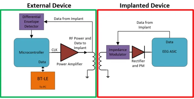
Figure 2-1 shows the high-level system diagram of the subdermal system for testing in a swine model, which consists of two parts - an external device that is placed on top of the skin, and an implanted device that will be surgically placed subcutaneously. Here the external device provides configuration data and power to the implant while also receiving EEG data to be relayed to a nearby device using BTLE. This design is described in more detail in 2.4. The implanted device design revolves around the ASIC described in 1.4.1 which provides the EEG analog front-end and digitization.
Figure 2-1: Subdermal System Diagram. External system block diagram is shown on the left. Implant System block diagram is shown on the right.
2.2 Changes From Previous Design
This design revision addresses several issues from the original design detailed in DoValle, where previous in-vivo pig tests failed after a few hours due to mechani-cal instability of the system [18]. This is largely attributed to the bulkiness of the devices used in the test setup. The revisions on the original design detailed in this document are aimed to reduce the physical size and increase the electrical efficiency of the entire system in hopes to streamline the device for longer term in vivo tests with pigs. The primary changes detailed here include a more efficient power amplifier de-sign, power management, optimization of impedance detection, use of Bluetooth Low Energy (BTLE), and an optimized external mechanical housing for animal survival and operator serviceability.
2.3 Implant Design
The main goal of the implant device design revision is further miniaturization and electronic robustness over the previous device in [18]. By reevaluating use cases of this device, many redundant systems from the previous design could be removed,
Figure 2-2: Previous Bonding Diagram for 144 pin LFCSP Package.
resulting in a smaller device. Furthermore, testing of the previous device revealed further optimizations for long-term electrical viability during in-vivo testing using pig models. The design revision has the following goals:
2.3.1 Electrical
ASIC
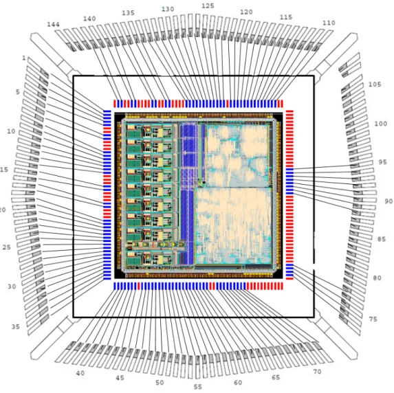
The original ASIC detailed in [18] is a 5mm x 5mm die fabricated using the TSMC 0.18 𝜇m process and packaged in a 20mm x 20mm 144 pin package. This package size was selected due to an uneven pad distribution on the die, resulting in one or more sides requiring more bondwires and an overall larger size as shown in 2-2. The ASIC contains two modes of operation. In Mode 1, EEG is constantly being sampled at the maximum clock rate and transmitted continuously to a receiving device. In Mode 2, sampling is reduced by a factor of 5 and data is only recorded to an off-chip SPI memory for later transmission when a seizure is detected.
For our application, seizure detection was not needed; thus, Mode 2 could be eliminated completely. By removing this mode of operation, many associated pads on the ASIC can be left unconnected and bond diagram can be balanced as shown in 2-3. With the reduced pad requirement, the ASIC can be fitted into a 9mm x 9mm QFN, minimizing overall device footprint. Figure 2-4 shows the result of the revised packaging.
Wireless Power Link
The device is powered by magnetically coupled coils at 2.5MHz with resonance in the secondary coil. A pre-fabricated 12.6𝜇H external receiver coil is placed in parallel with a 270pF capacitor as shown in Figure 2-5 as 𝐿1 and 𝐶1 respectively. This value
for the coil is selected in order to achieve the largest peak-peak voltage gain from external to implant and maximal load gain when reflecting an impedance from the implant to external device for communication. For a coupled coil system with an arbitrary coupling coefficient 𝑘, voltage gain is given by:
𝑉𝑜 𝑉𝑖 = 𝑘 √︁𝐿 𝑠 𝐿𝑝 1 + (1 − 𝑘2)𝑗𝜔𝐿𝑠 𝑍𝑠 (2.1)
Figure 2-5: Schematic for Implant Resonant Coil. 𝐿1, 𝐶1 forms a resonant tank for
power delivery. 𝐶2, 𝐶3, 𝑀1, and 𝑀2 modulate coil impedance for communication to
the external device. 𝐷1, 𝐷2, 𝐷3, and 𝐷4 form a bridge rectifier. 𝐷5 is a protective
where 𝐿𝑝 denotes the primary side inductance and 𝐿𝑠 denotes the secondary
induc-tance (𝐿1 in Figure 2-5) [19]. 𝑍𝑠 is the impedance across 𝐿𝑠. Assuming a capacitive
and resistive load across 𝐿𝑠, as is the case with a parallel resonant secondary coil
driving a load, voltage gain becomes: 𝑉2 𝑉1 = 𝑘 √︁𝐿 𝑠 𝐿𝑝 1 + (1 − 𝑘2)(𝑗𝜔𝐿𝑠 𝑅𝑙 − 𝜔 2𝐿 𝑠𝐶𝑠) (2.2) where 𝑅𝑙 is a resistive load and 𝐶𝑠 is the resonant capacitor across 𝐿𝑠.
Resonance is given by:
𝜔0 =
1
√︁
𝐿𝑒𝑓 𝑓𝐶𝑒𝑓 𝑓
(2.3) where 𝐿𝑒𝑓 𝑓, 𝐶𝑒𝑓 𝑓 are the effective inductance and capacitance respectively, which is
the rated inductance and capacitance added with any non-ideal or parasitic effects. At resonance, equation 2.2 combines with equation 2.3 to yield:
𝑉2 𝑉1 = 𝑘 √︁𝐿 𝑠 𝐿𝑝 1 + (1 − 𝑘2)(𝑗𝜔𝐿𝑠 𝑅𝑙 − 1) (2.4) which for very light loads (large 𝑅𝑙), becomes:
𝑉2 𝑉1 ≈ 1 𝑘 √︃ 𝐿𝑠 𝐿𝑝 (2.5) Reflected impedance from the 𝑅𝑙 across the primary coil 𝐿𝑝 from the coupled
resonant secondary with an arbitrary coupling constant at the resonant frequency is given by:
𝑍𝑟 = 𝑘2(
𝐿𝑝𝑅𝑙
𝐿𝑠
) + (1 − 𝑘2)(𝑗𝜔𝐿𝑝) (2.6)
where 𝑍𝑟 is the reflected impedance [20].
By selecting the largest value for 𝐿2, maximal voltage gain and largest load to
be reflected to the primary can be achieved; however, equation 2.3 suggests that larger inductor values would require smaller capacitor values for a particular resonant frequency. Having systems that depend on small value capacitors is a concern, as
Figure 2-6: Schematic for Implant Resonance Test. 𝐿𝑒𝑓 𝑓 = 𝐿1(= 12.6𝜇𝐻)+𝐿𝑝𝑎𝑟𝑎𝑠𝑖𝑡𝑖𝑐𝑠,
𝐶𝑒𝑓 𝑓 = 𝐶1(= 270𝑝𝐹 ) + 𝐶𝑝𝑎𝑟𝑎𝑠𝑖𝑡𝑖𝑐𝑠.
Figure 2-7: Implant Coil transfer Characteristic. Trough in curve represents the resonant frequency of the secondary coil.
parasitic capacitances, such as from inductor windings or diode reverse-bias junctions, start to cause a non-trivial and sometimes unpredictable variation in 𝐶𝑒𝑓 𝑓 from the
desired value. It should be noted that the 270pF 𝐶1 capacitor in Figure 2-5 is less
than what is expected to resonate at 2.5MHz to account for such parasitics. Due to manufacturing variations in the coil, the resonance of 𝐿1 with 𝐶1 was hand-trimmed
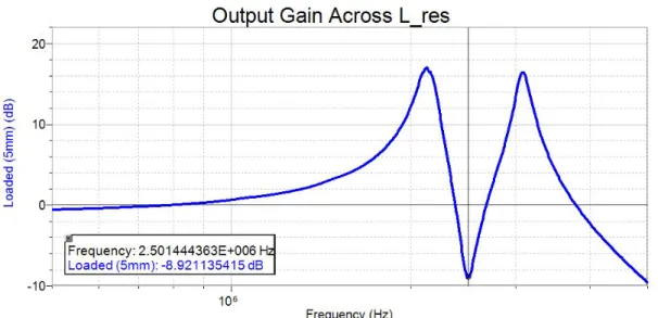
in the experimental setup by adding or removing small amounts of capacitance and measuring the frequency response with a network analyzer. The test setup schematic is shown in Figure 2-6. 𝐿𝑒𝑓 𝑓 and 𝐶𝑒𝑓 𝑓 is the resonant structure in the implant to be
trimmed. It should be noted that 𝐿𝑒𝑓 𝑓 and 𝐶𝑒𝑓 𝑓 is the desired resonant inductance and
capacitance respectively with non-idea parasitics added. 𝐿𝑟𝑒𝑠 and 𝐶𝑟𝑒𝑠 is an external
resonant tank set to resonate at the 2.5MHz operating frequency. The output is measured at 𝑉 _𝑜𝑢𝑡𝑝𝑢𝑡 relative to 𝑉 _𝑖𝑛𝑝𝑢𝑡. A sample gain plot used for trimming is shown in Figure 2-7. Trimming is achieved when the trough of the voltage transfer curve is at 2.5MHz.
AC current is then rectified by a bridge rectifier shown in Figure 2-5 as 𝐷𝐶/𝐷𝑎𝑡𝑎. Full-wave bridge rectification was chosen in order to keep the incoming AC signal symmetric to minimize distortion for the impedance-modulated link. Equation 2.4 suggests that the output voltage has a strong dependence on coupling coefficient 𝑘, which, is heavily dependent on relative coil placement and orientation. For our particular coupled coil system, 𝑘 ranges from approximately 0.08 to 0.35 over a range of 5mm to 15mm when coils are placed coaxially. This dependence causes large fluctuations in rectified voltage with positioning. In order to prevent large voltages from damaging downstream electronics, a 5.6V Zener 𝐷5is placed to clamp the output
voltage.
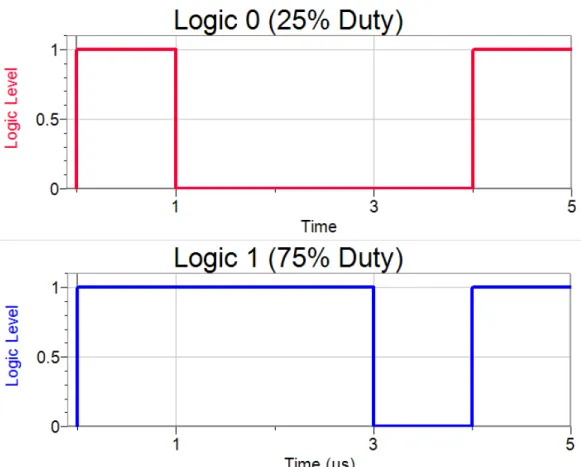
Uplink and Downlink Scheme
In order to both program the implanted ASIC and receive data from the implant to the external device, the data is encoded in an On-Off Keying (OOK) scheme. One bit of data is transmitted between rising edges of a signal where a duty cycle greater than 50% corresponds to a logic 1; likewise, a duty cycle less than 50% corresponds
Figure 2-8: Idealized On-Off Keying Scheme. Top shows a logic 0, bottom shows a logic 1. Data is encoded between rising edges.
to a logic 0. This type of data-encoding scheme was selected because it embeds both the data and clock information into a single channel such that synchronized clocks between transmitter and receiver are not needed. Ideally, the duty cycle should be as close to 75% and 25% for logic 1 and 0 respectively in order to have the greatest immunity against timing errors and non-idealities such as clock jitter and skew. In order to decode duty cycle, the receiving system simply counts how many cycles a reference clock has ’ticked’ between subsequent rising and falling edges corresponding to high and low times respectively. By simply comparing the two counts, a duty cycle estimation can be extracted. It should be noted that this reference clock needs to be several times the data rate in order to have sufficient resolution to compare high and low times as well as to have enough clock cycles to perform any calculation and transmit operation between data bits while not impacting subsequent bit counting. An example of the encoding scheme is shown in Figure 2-8.
In this design, OOK data transmission from the implant to external device is achieved by modulating the reflected impedance to the external device at approxi-mately 62.5KBit/s. MOSFETs 𝑀1, and 𝑀2 in Figure 2-5, in conjunction with large
value DC blocking capacitors 𝐶2 and 𝐶3, act as switches driven by 𝑈𝑝𝑙𝑖𝑛𝑘_𝑂𝑢𝑡,
pre-senting an AC short across power coil 𝐿1. This loading causes a drop in amplitude in
the external coil voltage, thereby amplitude-modulating OOK data on the external device power coil. Detection and demodulation of this signal is discussed in Section 2.4.1. This topology for load modulation was chosen since power is delivered to the implant when the gates 𝑀1 and 𝑀2 are tied to ground. This is important for cold
device startup since there is no bias voltage required to achieve resonance for power delivery - an issue in previous generation designs that caused a lockout fault and device failure after a period of time when not powered externally.
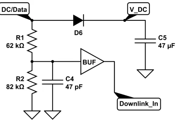
To pass data from the external device to implant in order to program the ASIC, OOK data is modulated onto the power link by turning on and off the external RF coil. Data is decoded by the implant device by monitoring the voltage level after the bridge rectifier as shown in figures 2-5 and 2-9 as 𝐷𝐶/𝐷𝑎𝑡𝑎. Here, node 𝐷𝐶/𝐷𝑎𝑡𝑎 is first voltage divided to a lower level so as to not damage the buffer, then low-pass
Figure 2-9: Schematic for Implant Decoder. 𝑅1, 𝑅2, and 𝐶4 filter the carrier ripple
and BUF is a Schmidt trigger input buffer for decoding.
filtered to remove carrier ripple while leaving the modulated data. Cutoff frequency for this filter is given by:
𝑓𝑐=
1 2𝜋(𝑅1||𝑅2)𝐶4
(2.7) the waveform is then fed into a Schmidt trigger input buffer in order to remove any additional noise and convert the waveform to a digital signal shown as 𝐷𝑜𝑤𝑛𝑙𝑖𝑛𝑘_𝐼𝑛. This signal is sent directly to the ASIC. For our system, data is coming in at approx-imately 10kbit/s on a 2.5MHz carrier with a typical DC rectified level around 3V. This results in a cutoff frequency range requirement that is less than the 5MHz ripple due to the bridge rectifier, but greater than 10KHz, and a resistor divider ratio of .75 to have an output around 1.8V. A cutoff of approximately 100KHz is selected by setting 𝑅1 to 62kΩ, 𝑅2 to 82kΩ and 𝐶4 to 47pF.
Capacitor 𝐶5 is the primary bulk storage capacitor for the system. Diode 𝐷6 is
Figure 2-10: Schematic for Implant Power Management. 𝐶5 and 𝐶6 are bulk storage
capacitors. TPS62736 is a buck converter, and LT3009 are low Iq linear regulators. Power Management
Further size reductions of the implant are realized through optimizations in on-board, off-chip power management. Through the elimination of Mode 2 from the ASIC, the device no longer is required to operate without an external power source as the power link also serves as the device’s communication link to stream the EEG data. This allows for the removal of the built-in lithium ion and associated charging electronics, yielding a simplified power scheme. This also eliminates a charging fault condition in the previous design where the battery could not be recharged if charge fell below a certain, level rendering this device unusable.
Because the implant will only be operational when an external device is providing power, internal energy storage elements can be kept at a minimum. For this design, the primary energy storage element is a capacitor shown as 𝐶5 in Figure 2-9 and
2-10. The only requirement for this capacitor is to ensure that the voltage at 𝑉 _𝐷𝐶 does not change appreciably when the external coil is off during ASIC programming. Assuming an extreme worst-case current consumption of 1mA and a worst-case du-ration that the external coil is off of 100𝜇s, total charge consumed is 100nC. For an ideal 47𝜇F capacitor, this results in a ripple of 2.1mV, or << 1% of the nominal 3V DC input level.
Figure 2-11: Implant PCB. Previous design with external coil attached (left). This work (right).
The ASIC itself requires 3 separate power supplies; a 1.8V supply and two 0.9V supplies for analog and digital. The unregulated DC voltage is first stepped down to 2.1V using a switching regulator. The TPS62736 is chosen for its light load efficiency and low quiescent current consumption as well as control outputs such as a "Power Good" (PG) signal that is used to hold the implant in reset until the output voltage has stabilized. To filter the voltage and remove any switching noise from the switching regulator and to step the voltage down further, a linear regulator first generates the 1.8V rail, then two more regulators generate the 0.9V. The LT3009 was selected for the linear regulators for its extremely low quiescent current.
2.3.2 Mechanical
PCB
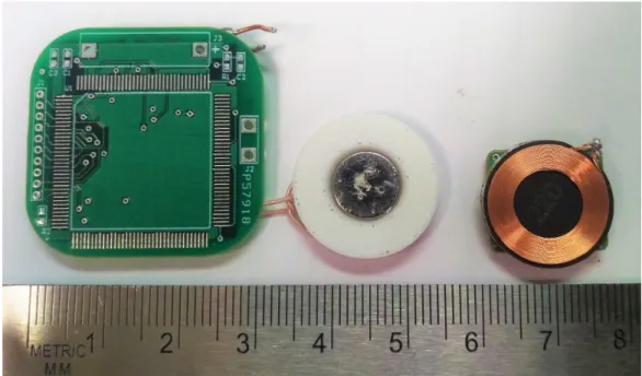
The aforementioned circuits are designed in Altium Designer and printed and as-sembled by Sierra Circuits. The board measures 14.0mm x 15.5mm. Three sets of
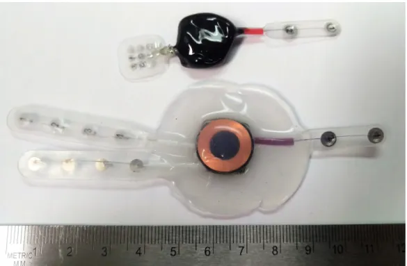
Figure 2-12: Coated Implant Devices. Epoxy coated1 (top), Parylene/Silicone coated
(bottom). channel.
In the previous design, the power coil was a handmade coil wound around a plastic holder using litz wire resulting in a thick coil due to the mechanics of the coil. Because of the thick size, the coil had to be placed adjacent to the implanted PCB, resulting in a very large implant footprint size. By moving to pre-fabricated coils using higher gauge magnetic wire, coil thicknesses and diameter can be minimized to the point that the coil can be stacked on top of the PCB for further miniaturization.
Figure 2-11 shows the completed PCB on the right. The electrodes and coil are soldered in place and bonded to the PCB using superglue. The overall result is a device that is roughly 10% the original size when the coil is added.
Fluid Barrier and Biocompatibility
In order to ensure the device remains functional while implanted, the device must be coated to prevent electrical shorting by body fluids. Two types of coating were
1Epoxy device shown has a 3x3 electrode array attached instead of the standard dual 1x4 electrode
Table 2.1: Electrical Properties of ParyleneN and MG Chemicals 832B Parameter Paryelene MGC 832B Resistivity (Ω/cm) 1.4 × 10¹³ 5.3 × 10¹² Dielectric Strength (V/𝜇m) 276 18.6 Dielectric 𝜅 @ 1MHz 2.65 2.77 Dissipation Factor @ 1MHz 0.6 × 10⁻³ 17 × 10−3
Figure 2-13: Parylene coated PCB - Top and Side Views. Features, ridges and over-hangs of the board are still clearly defined and visible.
tested. In the first test, the device was coated in MG Chemicals 832B Black Epoxy and Potting Compound, as shown in the left of Figure 2-12. The device was coated by repeatedly dipping the implant in a large container of epoxy until the desired coating thickness was achieved - until there were no remaining exposed contacts. The coating process was verified by ensuring the device remained functional while submerged in a saline solution.
However, during the first animal study, an electrical interaction with the pig tissue caused the power coil, 𝐿1 in Figure 2-5, to shift in resonance slightly, resulting in
reduced voltage and power transfer and inability to power on the device. This was likely caused by the high-frequency 2.5MHz carrier capacitively coupling into the pig’s tissue as a result of a too thin coating and relatively high dielectric constant, 𝜅, of the epoxy. Capacitive coupling into the pig shifts the impedance seen by the coil and moves the device away from resonance. In order to address capacitive coupling, the device was sent to VSIParylene to be professionally coated in 20𝜇m of parylene. Parylene is a standard coating for many medical implants and offers a much higher resistance and 𝜅 than the epoxy that was previously used. Table 2.1 compares the electrical specifications of MG Chemicals 832B epoxy with VSIParylene Parylene N coatings. Furthermore, parylene is applied using vapor deposition, which allows for a much more uniform coating on non-uniform surfaces than repeated dipping, thereby ensuring fewer openings for fluid ingress or capacitive leakage.
One pitfall of conformal coating via vapor deposition is that physical features or overhangs on the PCB will be covered, but still remain after coating, as shown in Figure 2-13. This means that any ridge or overhang will cause an air or fluid pocket when implanted, which heightens the risk of infection due to a lack of blood profusion in those pockets2. To address this, the device is coated in a silicone overmold in
order to fill in any ridges, overhangs and other features. The outer silicone overmold provides a featureless and smooth surface that conforms to the surface of the skull to reduce air and fluid pockets, while the inner parylene coating ensures a strong electrical and fluid barrier.
It should be noted that the surface energy of parylene is very low making the coating highly hydrophobic. This prevents many overmoldings, including silicone, to not adhere very well to the device. In order to increase the surface energy to allow for increased bonding with our silicone, the device is placed in an argon plasma chamber for surface etching. Because the high electric fields introduced by the plasma may damage the exposed electrodes, the electrodes were all connected together using copper tape and connected to ground in order to ensure no high fields were placed across any two electrodes.
To coat the device, the device is placed in a small shallow bowl and quick setting silicone is poured over the device. The device is then flipped and other side coated. The final parylene/silicone coated device is shown on the right of Figure 2-12.
In vivo testing of this device is described in more detail in Section 2.5.
2.4 External Device Design
Similar to the implant revision, the main goal of the external device design revision is further miniaturization and mechanical survivability during in-vivo experiments. Previous animal tests showed that the large physical size of the external device, due to large power requirements, irritated the pig during the experiment giving more resolve to remove and destroy the test setup. Additionally, the bulky external device required the battery and electronics to be mounted away from the head and connect to the transmit coil on the pig’s head via fragile tether cable. From the pitfalls of the previous animal experiments, the following design goals of the external device are derived:
∙ Miniaturized form factor that is self-contained entirely on the pig’s head. ∙ Efficiency optimized RF amplifier for lower power consumption.
Figure 2-14: Generic Schematic for Class-E RF Power Amplifier.
∙ Optimized mechanical housing that is more easily serviceable by technicians but impact proof.
2.4.1 Electrical
RF Power Amplifier
The previous design of the external device relied on a class-E amplifier to trans-mit power and data to the implant via magnetically coupled coils. Power and data delivery is discussed in Section 2.3.1. Class-E was originally chosen due to its the-oretical 100% efficiency and single phase clock requirement. However, in practice, the class-E power amplifier has a much more complex topology and relies heavily on matched impedances for optimal performance [21][22]. This becomes an issue when impedances are not tightly controlled. A generic class-E topology is shown in Figure 2-14. Equation 2.6 shows that the reflected impedance from the implant across the primary coil on the external device is a strong function of the coupling constant 𝑘. Since reflected impedance is changing not only for data modulation but, also coil
Figure 2-15: Schematic for Class-D RF Power Amplifier. 𝑀1and 𝑀2are the switching
elements. 𝐿1 is the external RF coil that resonates with capacitor 𝐶1. 𝐿2, 𝐶2, 𝐶3 and
𝑅1 form an input power filter for noise filtering
positioning, efficient power transfer using a class-E amplifier is exceedingly difficult. Furthermore, the class E amplifier exhibits a very large peak-peak voltage for low DC input voltages requiring very high current and low voltage power rails on the order of 0.5V, which is difficult to generate efficiently from a 3V supply.
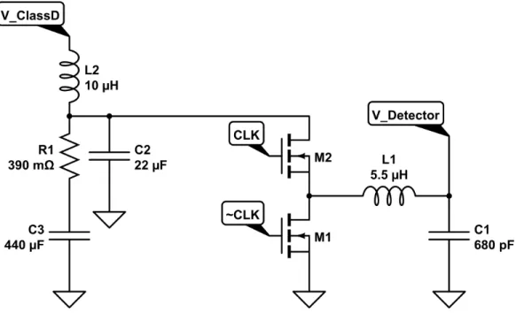
In order to address these issues in the previous design, a class-D topology is used as the power amplifier. The D is also a switching amplifier; hence, like the class-E, efficiencies 𝜂 > 90% can be theoretically achieved. Here, the class-D amplifier trades simplicity of design and matching for complexity in driving the amplifier - the design has only four primary components but requires a two-phase-shifted clock for optimal performance.
Figure 2-15 shows the schematic for the class-D power amplifier used in the ex-ternal design to power the implant. Inductor 𝐿1 is a 5.5𝜇H pre-fabricated transmit
coil that is magnetically coupled to the coil in the implant device (shown as 𝐿1 in
parasitics due to inter-winding capacitance and downstream electronics.
This filter gains the fundamental of a square wave generated by two NMOS switches, 𝑀1 and 𝑀2, which are stacked to form a “totem pole" structure. These
two switches are controlled by 𝐶𝐿𝐾 and its out-of-phase complement, ~𝐶𝐿𝐾, gen-erated by a micro-controller with a duty cycle slightly less than 50% in order to prevent shoot-through current - current from the power rail directly to ground when both switches are turned on simultaneously. The class-D can be turned off or on to signal data by stopping or starting the clocks that feed 𝑀1 and 𝑀2. It should be
noted that gate drivers are not needed for this design as the class-D supply voltage, 𝑉_𝑐𝑙𝑎𝑠𝑠𝐷 ≈ 1.2𝑉 , is significantly lower than the micro-controller ≈ 3.0𝑉 which is adequate to turn on high-side switch 𝑀2. Furthermore, small switching MOSFETs
are used that do not have significant gate capacitances as the total power dissipated by the class-D is only in the few 10’s of mW.
Similar to the implant device, the experimental setup requires manual trimming to account for coil manufacturing variation. To achieve this, peak-peak voltage output of the class-D amplifier is maximized during no-load operation by adjusting resonance capacitor 𝐶1.
Input Filter
Elements 𝐿2, 𝑅1, 𝐶1 and 𝐶2 in Figure 2-15 form a damped 2𝑛𝑑 order filter to prevent
current ripple injection back into the power supply from the high switching transients generated by the class-D. This is important, as the previous design showed that large current transients destabilized the feedback in upstream buck regulators that generate 𝑉_𝐶𝑙𝑎𝑠𝑠𝐷, thus lowering overall expected efficiency of the system. Here, 𝐿2 and 𝐶2
form a filter with a cutoff frequency around 10KHz, which is 2 orders of magnitude lower than the expected 2.5MHz injected noise. This ideally results in at least 80dB of attenuation of current noise rejection at 2.5MHz. In actuality, attenuation is closer to -50dB due to the use of non-ideal components yielding parasitic poles and zeros in the transfer function. In order to reduce the resonant peak generated by the LC pair, 𝑅1 is inserted to dampen the system. The value of 𝑅1 was determined through
Figure 2-16: Power Filter Transfer Function. LTSpice gain and phase simulation is shown in red, measured results are shown in blue.
simulation. 𝐶3 is placed as a large DC blocking capacitor to ensure no DC current is
shorted to ground. Performance of the filter was simulated in LTSpice using device models derived by manufacturer data and individual device testing. The experimental setup was verified on the final device using a network analyzer measuring the voltage transfer function from the power rail to the top of the switches. In this filter topology, the voltage transfer function from the rail to the top of the switches is the current transfer function from the top of the switches back into the power rail. Both the simulated and experimental results are shown in the gain-phase plots in Figure 2-16.
Detector
As described in Section 2.3.1, communication from the implant to the external device is achieved by impedance modulating OOK data across the implant coil, which is re-flected across the external coil. This change in impedance amplitude-modulates (AM)
Figure 2-17: Schematic for Differential Envelope Detector.
signal is passed through the differential envelope detector. A differential topology was selected for detection in order to keep the system symmetrical and to increase the signal-noise ratio (SNR) as compared to a single-ended envelope detector. This differential detector is shown in Figure 2-17.
Opposite-facing diodes, 𝐷1 and 𝐷2 rectify the negative and positive cycles of the
AM signal respectively. 𝐶4/𝐶5 and 𝑅2/𝑅3 form a filter to remove carrier ripple while
passing the OOK data. The resulting waveforms are AC-coupled by 𝐶6/𝐶7 to be
centered around a mid-rail voltage generated by 𝑅7, 𝑅8 and 𝐶9. Both differential
signals are fed into a comparator to convert to a single-ended digital output. Finally, 𝑅6, 𝐶8 and 𝐵𝑢𝑓 form a glitch filter in order to remove any glitches caused by carrier
ripple. The resulting digital signal is sent to an on board micro-controller for decoding. Waveforms from each step of the detector in the experimental setup is shown in Figure 2-18. It should be noted that Graph 5 demonstrates a glitch at 𝑡 ≈ 16𝜇𝑠 that is filtered out in Graph 6. It should also be noted that the output waveform pulse widths are slightly distorted when compared to the input OOK signal. This is due to the differential rectification step where the signal has an asymmetrical rise and fall time due to diodes 𝐷1 and 𝐷2.
Figure 2-18: External Detector Waveforms. From top to bottom: OOK Data, Detec-tor Input, Positive and Negative Envelope DetecDetec-tor, AC Coupled Envelope DetecDetec-tors, Comparator and Glitch-Filter Outputs, Final Output. Note that the final output pulse width is slightly skewed compared to the input due to decay times presented by the rectification step.
Overall, this topology allows decoding of asynchronous AM OOK data where the carrier amplitude and modulation depth can change continuously due to coil placement.
Digital Core and Communications
The external device contains a TI MSP430 micro-controller which handles the state-machine of the system and decoding of the data. The MSP430 series was selected due to their extremely low power consumption (<2.5mA typical at full load). In order to further optimize power, the MSP430 is kept in a sleep state for as long as possible. During operation, the micro-controller is held in sleep except for when an edge on the OOK data line triggers an interrupt. During the interrupt, the micro-controller only records the time since the last event and if the interrupt is a falling edge, compares the recorded times and writes the result to the UART. The micro-controller is placed in low-power sleep otherwise. C code is included in Appendix A.
The MSP430 communicates with a nearby laptop or RaspberryPi via a BTLE link connected via the UART lines. The previous design of the external device utilized a Bluetooth Classic radio for communication, which allowed for higher data rates, but required an order of magnitude more power to run and a much larger PCB footprint. By migrating to a DA14583 BTLE chip, power consumption and device size can be reduced. It should be noted that the DA14583 is using a custom, proprietary stack which only allows for phones or receivers running the same hardware and BTLE stack to communicate with it. This limitation is addressed in Section 4.1.1.
Power Consumption
Due to optimizations in Bluetooth communication and RF power amplifier design, power consumption of the device has been decreased by one order of magnitude: from 205mW in the previous design, to 32.1mW when transmitting and running from a 3V supply and implant device 1cm away. Measurements were taken by a Keithley Sourcemeter powering the device at the power input. Table 2.2 compares relevant
Table 2.2: Power Consumption of External Device. Devices measured at 3V, 1.0cm coil distance, and transmitting to a receiver.
Block Previous Design(mW) This Work(mW)
Micro-controller 7.5 6.0
Bluetooth 87 8.3
RF Power Amplifier 42 16.6
Analog Components + PMIC 703 1.2
Total 205 32.1
sub-blocks of the previous design with this work. Battery Selection
Previously, the high power consumption of the external device required a large battery to be used which made the device overly large and bulky. For this design, we aim for a runtime of approximately 100 hours using a 3Wh battery. It should be noted that the external device requires a constant current draw of approximately 10mA if powered by a 3V source. Although the largest 3V commercial button battery, CR2477, has the capacity needed and would provide an optimal shape and size to power this device, Lithium Manganese Dioxide (Li-MnO2) cells have a nominal current draw in the 100’s
of 𝜇A and cannot be used for this application. A Tadiran 1/2AA lithium ion battery was selected to power this device. The battery has a nominal capacity of 3.9Wh while suppling a continuous current in excess of 10mA. The cylindrical battery measures measures 14.5mm dia x 25.0mm and should last for approximately 120 hours.
2.4.2 Mechanical
PCB
The electronics were printed on a PCB shown in Figure 2-19 on the right. The board measures 22mm in diameter. Similar to the implant device, the transmit coil is a
Figure 2-20: External Device Enclosure. 3D Render (left), 3D Printed (right). prefabricated coil using high gauge wire resulting in a very thin package that can be stacked on top of the PCB to reduce device footprint.
Enclosure
Previous designs used in in-vivo animal tests relied on a backpack-mounted enclosure with a tether wire from the electronics to the transmit coil located pig’s head. This tether was frequently damaged, causing the experiment to fail. Because of the reduced board size and power consumption allowing the use of smaller batteries, cumbersome enclosures to encompass the external electronics are no longer needed and the battery, board, and transmit coil can all reside on the pig’s head eliminating the need of a tether wire.
In order to achieve this, an enclosure was designed with the help of Nevan Hanu-mara, Ph.D and Daniel Teo, Ph.D. 3D renders of the enclosure showing battery (purple, top), PCB (green, middle) and transmit coil (black, bottom) with mounting plate is shown in the left of Figure 2-20. 3D prints of the device are shown on the right. A baseplate is mounted on the pig and the electronics package is mounted on the baseplate via a quarter turn-lock secured by magnets for quick removal and
Figure 2-21: Operating Room Theater for Pig Implantation.
pig. Figure 2-24 shows the device mounted on the pig. The enclosed external device measures 30mm in diameter and 22mm in height.
2.5 Animal Testing
The implant was tested in-vivo using 50kg swine at Massachusetts General Hospital (MGH). Tests were performed on two different pigs named Snowball and Kevin. Figure 2-21 shows the operating theater for implantation.
2.5.1 Pig 1: Snowball
The pig is first anesthetized and an approximately 6cm x 9cm U-shaped incision is made right above the nuchal crest on the head of the pig. An epoxied device is placed down on top of the skull with the eight electrodes pointing towards the nose of the pig and ground and reference electrodes folded to the rear. The device and electrodes are glued down to the periosteum of the skull. The skin flap is replaced over the
Figure 2-22: Pig 1 implantation surgery showing electronics package (black) and 8 electrodes (yellow, brown).
surgical area and device is tested a final time before closing the incision. Finally, the external device baseplate is sutured down to the skin right above the implant, and the external device mounted in the baseplate and pig allowed to wake up.
Unfortunately, shortly after closing up the pig, the external device stopped being able to communicate with the implant. This was caused by the minimum gap be-tween the coils exceeding the experimentally validated 5mm. By placing the coils too close together, coupling constant 𝑘 becomes much larger than expected and reflected impedance across the external coil drops as shown in equation 2.6. This places a larger load across the external coil and causes the amplitude to drop. Furthermore, equation 2.4 suggests a higher 𝑘 also decreases voltage gain across the coils which holds the implant in a reset state due to too low of a rectified voltage. This change in minimum operating distance is likely caused by capacitive interactions with the pig’s tissue which shifted the resonant frequency of the implant coil; however, this cannot be verified as the epoxy coated device cannot be probed once coated. In order to resurrect the device, the external device’s peak-peak voltage level across the transmit
Figure 2-23: EEG Data from Pig 1. Only channels 0-3 are shown. Time domain is shown on the left, power spectrum is shown on the right.
about an hour and half. A sample of this data is shown in Figure 2-23.
Figure 2-24 shows the external device on top of the pig. Because the external device is now on the pig’s head, the device becomes more prone to impact and liquids, as the pig has more freedom to hit the device against the pen’s walls as well as soak the device when drinking water from an overhead spigot. This caused the device to fail again after an hour and half into testing due to water ingress into the external device, shorting out the electronics. The device was then removed from the pig and inner chamber, which holds the electronics, filled with epoxy to waterproof.
The device was again placed on the pig’s head but failed after 30 minutes. It was initially thought that the failure stemmed from the sutures that held the baseplate to the pig’s head coming lose and moving significantly, but after reattaching the external device, the implant still remained unresponsive. Connecting a spectrum analyzer to an external coil showed that resonance of the implant device had not changed significantly and that power transfer was being achieved, but device not responding indicating that the implant itself was electrically dead and could not be recovered.
Figure 2-25: Pig 2 implantation surgery showing the silicone encapsulated device. The pig was euthanized and device explanted. It should be noted that this particular implant did not have the protective Zener diode shown as 𝐷5 in Figure 2-5. Because
of this, it is likely that an overvoltage condition damaged the buffer in Figure 2-9. This overvoltage condition was likely caused by the loose device causing the two coils to move significantly relative to each other. This movement changes the 𝑘 between the implant and external coil which, in addition to the increased peak-peak voltage of the external device, can cause large voltages in the implant device as suggested by equation 2.4.
2.5.2 Pig 2: Kevin B.
From analysis of the failure mode from the first pig, the system was modified to be more electrically robust to the in-vivo environment. In order to address the possible capacitive tissue interaction causing changes in the resonant properties of the implant device, the implant was sent to be professionally coated in parylene as described in Section 2.3.2. Additionally, Zener diode 𝐷5 in Figure 2-5 was added to protect against
possible overvoltage conditions. Finally, resonance on the implant side was adjusted slightly to compensate for thinner pig skins. The effective range of the device now is
Figure 2-26: Pig 2 with External Device. 3mm to 12mm from the original 5mm to 15mm.
The implantation procedure remained largely the same as the previous experiment. Figure 2-25 shows the new device being implanted. In order to fortify the sutures such that the external device does not fall off like in the previous experiment, sutures were drawn through the entire skin flap instead of just through the first few epidermal layers. Additionally, a rubber sheet was placed over the external device and sutured down in order to reduce the strain on the primary sutures. The external device is shown in Figure 2-26.
In this trial, the system was able to collect data for approximately 2 and half hours, with a gap in data due to a battery change. Unfortunately, communication to the implant was lost afterward due to not enough voltage reaching the implant. It is hard to determine the exact root cause of this failure, but one possibility is that swelling of the skin caused the coils to move further apart, beyond the 12mm range. In
Figure 2-28: Cross section view of the implant under the skin. Skin is shown in orange, device in grey, skull in blue. Pockets are formed on the left and right of the implant underneath the skin shown in green.
pig had developed a severe infection and had to be euthanized thereby terminating the experiment. Figure 2-27 shows the infected area on the pig. The discolored skin is narcotizing tissue and pus with the implant being exposed on the left side of the incision.
It is likely that this infection is due primarily to the shape of the implant. Be-cause the pig’s skin is not extremely malleable, placing a semi-rigid object under an otherwise flat surface and covering it with a skin will form a lump on the surface of the skin. This deformation causes air and fluid pockets to form around the implant between the skin and skull as the device pushes up on the skin. The formation of the air pockets are shown in Figure 2-28. Such air and fluid pockets are not ideal for long term implants, as these regions are void of any vascular systems and therefore have no blood supply. Without blood perfusion, antibodies cannot reach these areas and fight any infection should they occur. By modifying the external shape of the implant to conform more closely to the skull and skin, these void pockets can be avoided thereby minimizing the risk of infection.
2.6 Data Analysis
Figure 2-29: Bipolar Pig Waveforms. Top graph is a region selection. Middle two graphs are unipolar channel 1 and channel 2 plots and spectrums. Bottom two plots shows bipolar plots and spectrums between channel 1 and 2 and channel 1 and 3.
domain waveforms. For example, a pig under or just waking up from anesthesia is likely to have predominately low frequency (< 8Hz) waveforms though, a precise correlation is difficult without a very detailed record or video of the pig’s actions while being recorded. Because the device records EEG as a unipolar measurement (referential montage), the data must be first converted to a bipolar measurement by subtracting EEG channels from each other. This aids in waveform analysis and landmark identification by removing noise caused by the reference channel. Since unipolar measurements are all referenced to a single reference electrode, any noise from the reference electrode such, as muscle or eye movements, will produce artifacts in all the channels. Figure 2-29 shows both unipolar and bipolar plots. The middle two plots are unipolar plots for channel 1 and 2 and show almost identical waveforms and spectrums. The bottom two plots are bipolar plots between channels 1 and 2, and 1 and 3 respectively. These bipolar plots are computed by taking the difference between the unipolar measurements of the respective channels. It should be noted that the high frequency oscillation in the unipolar plot near time 2285s is likely caused by muscle interference and appears across all unipolar measurements; however, bipolar plots 1-2 and 1-3 eliminate this interference and look markedly different from each other and from the unipolar measurements.
Chapter 3
Wearable System
This section details the design of major components that comprise the wearable sys-tem. The design of this wearable EEG patch has the following functional require-ments:
∙ Rapid application of sensors to access EEG from the frontal and prefrontal cortexes (forehead).
∙ Comfortable recording for at least 72 hours.
∙ No dependence with surrounding environment (e.g wires to a large module, dependence on outlets, sockets, etc.)
∙ Real time and historical data monitoring.
∙ Minimal EEG noise and interference from the environment.
3.1 System Overview
Figure 3-1 shows the system block diagram of the wearable EEG system. Prefab-ricated electrodes are connected to the ASIC described in Section 1.4.1 with the modifications detailed in Section 2.3.1. A microprocessor is directly connected to the
Figure 3-1: Wearable System Block Diagram showing the main functional components of the patch EEG.
Figure 3-2: Schematic for Wearable ASIC Communication. ASIC and MSP430 are now electrically connected together and share common clocks.
3.2 Design
At a high level, the design of this system is remarkably similar to the subdermal design without the coupled coil communication; the same ASIC originally intended for the aforementioned subdermal EEG system is repurposed for this wearable design.
3.2.1 Electrical
Communication and Microprocessor
In order to program and receive data from the ASIC, the same MSP430 series mi-croprocessor is used. Figure 3-2 shows the primary control signals between the ASIC and microprocessor. Because the ASIC is no longer physically separate from the
mi-croprocessor, it is not necessary to rely on the OOK communication scheme described in Chapter 2.3.1. Moving away from OOK has advantages in power consumption as detailed in Section 3.2.1.
The ASIC allows for SPI communication originally intended for bench-top testing in order to read and write data directly to the chip without using the OOK pins. This communication can be leveraged in order to reduce the processor requirements and simplify the overall system. It was originally intended that SPI or OOK commu-nication could be selected between via an external digital pin on powerup shown as 𝑂𝑂𝐾/𝑆𝑃 𝐼_𝑆𝐸𝐿𝐸𝐶𝑇 in Figure 3-2. However, an error in the chip disabled the SPI interface regardless of the state of the select pin. In order to circumvent this issue, it was discovered that data could be received using the SPI interface if the select pin was set after the ASIC is first programed using OOK via direct electrical connection to the pins. After SPI data is received by the microprocessor, the data is streamed over BTLE to the same base station used in the subdermal system.
In order to increase flexibility of the wearable system and reduce power consump-tion dynamically, the ASIC’s main clock is sourced from the microprocessor directly instead of being set by an external resistor. By allowing the microprocessor to control the system clock of the ASIC, the microprocessor can change the sample rate of the ASIC in order to achieve higher bandwidth recordings or minimize power consump-tion depending on the needs of the user. The upper sapling rate of this system is only limited by the maximum data rate of the BTLE module, which for this particular radio is 88.9kBit/s. At 56 bits per sample for this 4-channel device, the maximum achievable sample rate is 1.58KHz.
Power Consumption and Optimization
Figure 3-3 shows the power consumption of relevant blocks of the wearable EEG system. The device was measured using a benchtop power supply connected to an Agilent Technologies benchtop digital multimeter. The supply was set to 1.4V and
Figure 3-3: Wearable Power Consumption Breakdown. Measured at 1.4V at input to the system sampling at 542Hz. Total power consumption is 6.8mW.
Figure 3-4: Diagram for power management on the wearable device showing locations and generation of all the relevant voltage domains.
![Figure 1-2: 10-20 Electrode System Placement [12]. Electrodes are placed in incre- incre-ments of 10% and 20% of the front-back or left-right distance of the skull.](https://thumb-eu.123doks.com/thumbv2/123doknet/14682007.559464/19.918.177.746.114.413/figure-electrode-placement-electrodes-placed-incre-incre-distance.webp)