HAL Id: tel-00779495
https://tel.archives-ouvertes.fr/tel-00779495
Submitted on 22 Jan 2013HAL is a multi-disciplinary open access archive for the deposit and dissemination of sci-entific research documents, whether they are pub-lished or not. The documents may come from teaching and research institutions in France or abroad, or from public or private research centers.
L’archive ouverte pluridisciplinaire HAL, est destinée au dépôt et à la diffusion de documents scientifiques de niveau recherche, publiés ou non, émanant des établissements d’enseignement et de recherche français ou étrangers, des laboratoires publics ou privés.
Structural, optical and electronic properties of InN films
and In rich heterostructures for optoelectronic
applications
G. R. Mutta
To cite this version:
G. R. Mutta. Structural, optical and electronic properties of InN films and In rich heterostructures for optoelectronic applications. Materials Science [cond-mat.mtrl-sci]. Université de Caen, 2012. English. �tel-00779495�
UNIVERSITÉ de CAEN BASSE-NORMANDIE
U.F.R.: Sciences
ECOLE DOCTORALE: Structure, Information, Matière et Matériaux
THESE
Présentée par Geeta Rani MUTTA
et soutenue le 27 juin 2012 en vue de l’obtention du
DOCTORAT de L’UNIVERSITÉ de CAEN
Spécialité: Milieux denses, matériaux et composants
Propriétés structurales, optiques et électroniques des
couches d'InN et hétérostructures riches en indium pour
applications optoélectroniques
MEMBRES du JURY
M. Régis CARIN M. Laurent PICHON
Professeur, Université de Caen Professeur, Université de Rennes
Président du jury Rapporteur
M. Philippe VERMAUT Maître de conférences, ENSCP, Paris Rapporteur
Mme Eva MONROY Ingénieur CEA, INAC, Grenoble Examinateur
M. Philippe de MIERRY Chargé de Recherche, CRHEA, Valbonne Examinateur
M. Jean-Louis DOUALAN Chargé de Recherche, CIMAP, Caen Examinateur
M. Jean-Marc ROUTOURE Professeur, Université de Caen Co-directeur de thèse
Dedicated to my father Late Mutta Narasinga Rao
There is not a more pleasing exercise of the mind than gratitude. It is accompanied with such an inward satisfaction that the duty is sufficiently rewarded by the performance
v
Acknowledgements
The work presented in this dissertation has been carried out at CIMAP and GREYC laboratories during the period 2009-2012. My thesis entitled: “Structural, optical and electronic properties of InN thinfilms and In rich heterostructures for optoelectronic applications” has been performed in the frame work of the European Union project RAINBOW. Behind the accomplishment, there is a number of people, who helped to make it possible and I take this opportunity to express my special gratitude to them.
First of all I express my deep gratitude to my Ph. D advisors, Dr. Pierre Ruterana and Prof. Jean Marc Routoure, who have given me the opportunity to work with them when they choose me for the Marie Curie Fellowship. They introduced me to the field of Transmission Electron Microscopy and low frequency noise techniques, their ideas and guidance have been invaluable. I thank them for providing me with useful comments and directions in order to improve my research. They provided me numerous opportunities to give presentations, encouraged logical, problem solving and gave me confidence whenever I needed it. I am very grateful for the freedom I was given during the project and the constant encouragement when I felt it was all going wrong! I am always amazed at their reduction of complex problems to its simplest and specially to accomplish the deadlines in short time. I am also glad of the opportunities to learn about the administrative matters in addition to scientific work. I express my extended thanks to Dr. Ruterana for rewriting the French part of Ph. D thesis.
I wish to express my sincere thanks to the members of my Ph. D Jury: the President Prof. Regis Carin, the reviewers: Prof. Laurent Pichon and Dr. Philippe Vermaut; the examiners: Dr. Eva Monroy and Dr. Philippe de Mierry, firstly for accepting to judge my work and for their constructive comments which enhanced the manuscript to its present shape.
I owe a great deal of thanks to Dr. Laurence Mechin and Dr. Bruno Guillet, who were very supportive and always entertained my questions in every aspect of learning from conducting experiments to analysing the data and also to make critical comments which helped me to understand better the concepts of precision in measurements, knowledge in device fabrication and many more.
I express my gratitude to Prof. Jean Louis Doualan for teaching me to conduct optical measurements. I enjoyed his help, guidance, insight and humour all these years.
I am very much grateful to Dr. Magali Morales, Dr. Phillipe Marie, Prof. Christian Dufour and Dr. Fabrice Gourbilleau for rekindling my interests in crystallography, semiconductor physics, quantum mechanics, nanotechlonogy and proving that learning can be fun. I extend my sincere thanks to Dr. Serge Bouffard, head of the Laboratory, for having accepted me in CIMAP; he has always been a source of encouragement through the tough times with administrative matters.
vi
I convey my special thanks to Marie-Pierre Chauvat, who was always available for teaching me the sample preparation for TEM and to fix my computer so often. I also thank Cédric Fur for showing me the device fabrication steps on InN layers. I thank Dr. Bertrand Lacroix for STEM measurements and also for his fruitful scientific discussions.
Huge thanks to the RAINBOW family members with whom I built good collaboration all along the past three years and for exchanging the scientific ideas, as well as spending good times in workshops and conferences. Additionally, I express here my sincere thanks to Prof. R. Goldhahn and Prof. F. Calle for letting me visit their groups and giving the time for insight during scientific discussions.
I was really lucky to have perfect Ph.D students, who provided assistance to me during my work, especially Arantxa, Céline ,Yi, An, Chang hui from CIMAP and Dalal ,Shuang, Sheng, Rachida and Hakim from GREYC. I specially thank Pratibha, with whom I shared special memories in Caen.
I extend my heartfelt thanks to Yadira for her cordial scientific and social discussions with me. I acknowledge Pierre Mathieu, Julien, Cédric, Michael, Stéphane and Nicolle for the good times spent at lunches and also for putting a large effort in hearing and correcting my French.
My special thanks to Elodie, Delphine, Nicolle Chasle and Claire, for their indispensable aide concerned with travel, administration and bureaucratic matters efficiently during my stay.
I shall be morally failing if I do not express my thanks to Larysa and Vladimir, who were always available for scientific discussions as well as to give me a constant co-operation and moral support during my stay here in Caen.
Many thanks to all of the past and present colleagues of CIMAP and GREYC, for making nice and jovial working atmosphere. To all of you, thanks for making my time in Caen, a great experience both in the lab and in the outside world.
My special thanks to Srinivas, Uma Mahesh and Jyothi, for having a lot of interesting and intellectual debates and also for being very supportive whenever I needed.
I pay respect to my family members, who have been great over the years. Without their whole hearted support, love and encouragement I would not have been here. Finally, I thank my angel niece: Swetha, for her unconditional love and affection towards me.
vii
CONTENTS
Résumé xi
Introduction xvi
Chapter 1 1
Introduction to III-nitride semiconductors and low frequency noise
1.1 Brief History of Nitrides 1
1.2 Properties of III nitride semiconductors 2
1.2.1 Crystalline structure 2
1.2.2 Crystal polarity 3
1.2.3 Dislocations 4
1.2.4 Spontaneous and piezoelectric polarization 5
1.3 Group III nitrides epitaxy 8
1.3.1 Substrates and buffer layers for group III nitrides 9
1.3.1.1 Sapphire substrate 10
1.3.1.2 Silicon carbide (SiC) substrate 10
1.3.1.3 Silicon substrate 10
1.4 Applications of group III nitrides 11
1.4.1 Optical applications 11
1.4.2 Electronic applications 12
1.5 Low frequency noise 13
1.5.1 Noise definition 13
1.5.2 Noise spectral density 14
1.5.3 White noise sources 16
viii 1.5.5 1/f noise sources 17 1.5.6 1 /f noise models 18 1.6 References 19 Chapter 2 23 Experimental techniques 2.1. Growth techniques 23
2.1.1Molecular Beam Epitaxy (MBE) 23
2.1.2Metal Organic Vapor Phase Epitaxy (MOVPE) 24
2.1.3Epitaxial layers used in this dissertation 24
2.2 Samples characterization 25
2.2.1 Microscopy techniques 25
2.2.1.1 Atomic Force Microscopy (AFM) 25
2.2.1.2 Electron microscopy 27
2.2.1.2.1 Scanning Electron Microscopy (SEM) 28
2.2.1.2.2 Transmission Electron Microscopy (TEM) 29
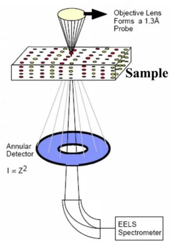
2.2.1.2.3 Scanning Transmission Electron Microscopy (STEM) 33
2.2.1.2.4 TEM sample preparation 34
2.2.2 Optical characterization 37
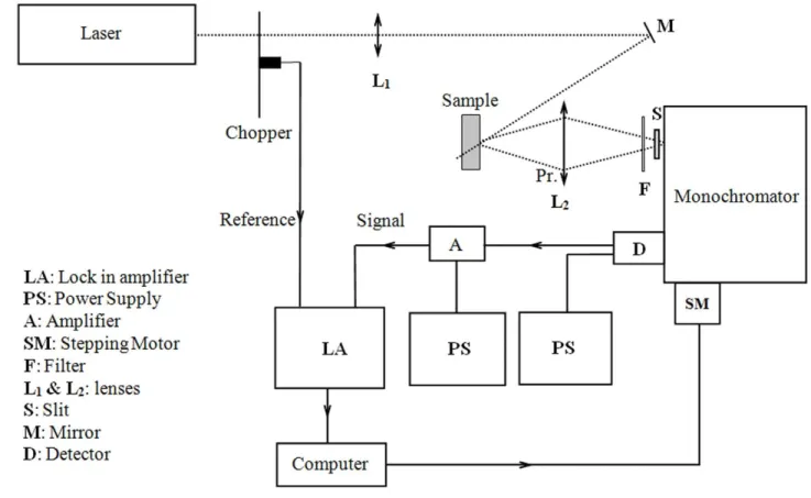
2.2.2.1 Photoluminescence spectroscopy (PL) 37
2.2.3 Electrical characterization 39
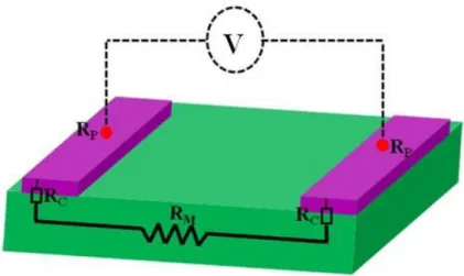
2.2.3.1 Probe Stations 39
2.2.3.2 Peripheral apparatus 41
2.2.3.3 Current-Voltage (I - V) and resistance measurement 41
2.2.3.4 Instrumentation for DC measurements 45
2.2.3.4 Instrumentation for DC measurements 46
ix
Chapter 3 49
Plasma Assisted Molecular Beam Epitaxial InN layers electrical conduction
3.1 Introduction 49
3.1.1 PAMBE growth regimes of InN 50
3.1.2. Transport properties of indium nitride 51
3.2 Objectives of this research 54
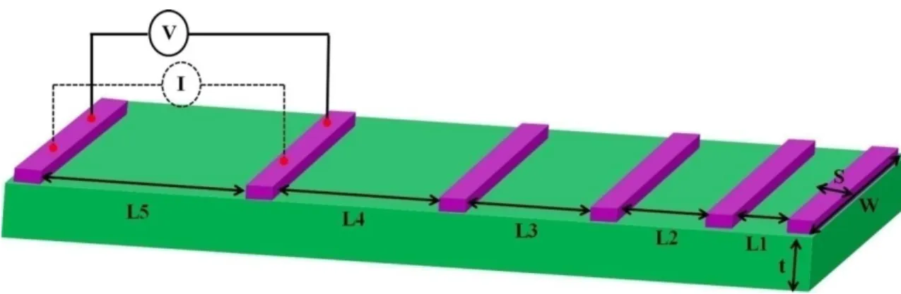
3.3 Description of samples 54
3.3.1 Samples schematic 54
3.3.2 Samples geometries and fabrication process 56
3.4 Effect of processing modulation on electrical performances 59
3.4.1 Characterization 59
3.4.1.1 Surface morphology by AFM and SEM 59
3.4.1.2 Photoluminescence characteristics 60
3.4.1.3 Electrical properties studies at room temperature 61
3.5 In and N rich InN layers 66
3.5.1Surface morphology 65
3.5.2 Electrical properties studies at room temperature 66
3.5.3 Electrical properties studies with temperature 69 3.6 Conclusions 74
3.7 References 75
Chapter 4 78
InGaN Quantum wells: Transmission Electron Microscopy and Photoluminescence studies 4.1 Introduction and Motivation 78
4.1.1 Effect of polarization fields in InGaN/GaN QWs 78
x
4.2 Samples 83
4.3 Microstructure studies of InGaN QWs for V-pits and its association with PL studies 84
4.3.1 Microstructure 84
4.3.2 Optical properties of InGaN/GaN QWs 87
4.4 Microstructure analysis with CTEM, HRTEM and STEM: 90
4.4.1 Microstructure and chemical composition studies with HRTEM 90
4.4.2 HAADF Investigations 93
4.4.3 Comparison of extracted In composition with literature 94
4.5 Conclusions 96
4.6 References 97
Chapter 5 102
Conclusions and perspectives
5.1 InN layers 102
5.1.1 Conclusions 102
5.1.2 Open questions and future work 103
5.2 InGaN/ GaN QWs 104
5.2.1 Conclusions 104
5.2.2 Open questions and future work 104
5.3 References 106
Annex I 106
xi
Résumé
Au cours des deux dernières décennies, les semi-conducteurs nitrures (AlN, GaN, InN) ont été sujets à des recherches très intenses en raison des nombreuses applications (diodes électroluminescentes (LED), transistors de puissance, composants hyperfréquences, etc, ..). L'effort de recherche s'est amplifié depuis 2002, quand la bande d'InN a été réévaluée à 0,65 eV au lieu de 1,89 eV, admis auparavant pendant plus de 20 ans. Cette découverte à ouvert la voie aux nitrures pour la possible fabrication des LED multicolores qui devraient couvrir les gammes de longueurs d’onde de l'UV lointain au proche infrarouge avec des applications très attendue dans l'éclairage faible consommation par exemple. De plus, le semi-conducteur InN présente une mobilité d'électron de plus de 4000 cm2V-1s-1 ce qui pourrait aussi constituer une plateforme pour le développement de composants électroniques fonctionnant jusque dans la gamme terahertz. Actuellement, la qualité des couches d'InN n'est pas encore optimale et beaucoup d'efforts de recherche sont encore nécessaire pour améliorer et comprendre ses propriétés.
Mon travail doctoral s'inscrit dans cette dynamique et porte sur « les propriétés structurelles, optiques et électroniques de films d'InN et hétérostructures riches en indium ». Il a été effectué dans les laboratoires de CIMAP et GREYC dans le cadre du projet RAINBOW Initial Training Network du 7ème Programme Cadre de Developpement Européén de la section People". Le projet RAINBOW (2008-2012) avait comme objectif la réalisation « des couches d'InN de qualité optimale et l'investigation des propriétés intrinsèques d'InN et d'alliages de nitrures riches en indium ». Il consiste en une étude des dispositifs en corrélation avec les propriétés structurales. A cet effet, deux dispositifs ont été abordés: 1) des composants, mis en forme par des techniques de photolithographie, dans des couches d'InN fabriquées par épitaxie aux jets moléculaires assistée par plasma, 2) des puits quantiques InGaN/GaN qui constituent les zones actives des diodes électroluminescentes et des diodes lasers. Dans le premier cas, nous avons cherché à accéder à la conduction de volume d'InN car ses propriétés remarquables ne sont pas encore exploitées à cause d'une accumulation intrinsèque de charge aux surfaces. Pour se faire, nous avons utilisé des mesures du bruit basse fréquence.
Le deuxième volet de ce travail s'est inscrit dans l'analyse des mécanismes qui pourraient expliquer la forte efficacité d'émission bleue dans les puits quantiques InGaN/GaN
xii
malgré les fortes densités de défauts (>108cm-2). Pour se faire, nous avons analysé la structure, la chimie et la morphologie des puits quantiques en fonction des conditions de croissance. Ces données ont été corrélées avec les propriétés optiques.
Le manuscrit est divisé en cinq chapitres. Le premier chapitre est divisé en deux sections. La première section constitue une brève description des propriétés et applications des semi-conducteurs nitrures et leurs alliages. Leur structure cristalline la plus stable est la structure wurtzite qui n'est pas centro-symétrique. Par conséquent, les couches ont une polarité de cristal N ou métal et les surfaces correspondantes présentent des propriétés très différentes. Les techniques principales de croissance des nitrures sont l'épitaxie aux jets moléculaires (MBE) et l'épitaxie en phase vapeur aux organométalliques (MOVPE). Les substrats communément utilisés pour dépôt des nitrures sont le saphir, le carbure de silicium et le silicium. Comme la structure wurtzite est polaire, il existe un moment dipolaire qui engendre un champ de polarisation spontané le long des directions polaires. En plus, une polarisation piézoélectrique est produite par la tension aux interfaces dans toute l’hétéroépitaxie. Ces champs de polarisation affectent les performances des dispositifs. Ils peuvent être diminués par un choix judicieux de l'orientation de croissance des couches. Au cours de ce travail, nous avons seulement étudié des couches épitaxiées le long de la direction polaire [0001]. La deuxième section du 1er chapitre porte sur l'analyse des matériaux et dispositifs par mesures du bruit basse fréquence. Ces mesures constituent un outil de diagnostic pour explorer les propriétés mésoscopiques et/ou microscopiques des matériaux, car le niveau et le type de bruit est très sensible aux processus de transport. En effet, le bruit intrinsèque dans un système électrique résulte des fluctuations spontanées dans la conductivité électrique. Il est mesuré en termes de fluctuations sur la tension à travers les terminaux de l'appareil ou dans le courant qui y circule. Ces fluctuations peuvent être analysées dans le domaine spectrale à l’aide de la densité spectrale de bruit contenant généralement trois contributions : le bruit blanc, le bruit Lorentzien et le bruit en 1/f. Les mesures de bruit présentaient, pour nous, un intérêt considérable car I) le niveau de bruit est un indicateur sensible de la qualité du matériau et II) il fournit, par la comparaison avec les modèles théoriques, une façon de déterminer les mécanismes dominants de conduction.
Dans le deuxième chapitre, nous avons décrit premièrement les deux techniques de croissance les plus utilisées pour la réalisation des couches épitaxiales des nitrures et ensuite les techniques expérimentales utilisées pour caractériser les hétérostructures d'InN et InGaN/GaN. Nous avons utilisé une série de techniques de microscopie (AFM, SEM, TEM,
xiii
HRTEM et STEM) pour déterminer la rugosité de surface, la morphologie, la microstructure ainsi que la composition dans puits quantiques InGaN/GaN. Le principe et le mode d'opération de chaque technique ont été exposés ainsi que les méthodologies pour la préparation d'échantillons de TEM. La caractérisation de la photoluminescence a été mise en œuvre pour analyser les propriétés optiques des couches d'InN et des puits quantiques InGaN/GaN. Les propriétés électriques de transport dans les couches d'InN ont été mesurées sur une gamme de température s’étendant de celle de l’azote liquide jusqu’au température ambiante. Les détails des dispositifs expérimentaux permettant d’effectuer les mesures électriques notamment l’estimation de la résistivité et la mesure de bruit basse fréquence sont également exposés dans ce chapitre.
Le troisième chapitre discute les résultats des mesures de bruit de basse fréquence dans les couches d'InN produite par épitaxie aux jets moléculaires (EJM). En ce qui concerne la fabrication des structures par les techniques classiques de la microélectronique (photolithigraphie, dépôt, gravure, etc.), nous avons d'abord montré que le recuit thermique devait intervenir après les étapes de la gravure et de dépôt des métaux utilisés pour assurer les contacts électriques.
Le niveau de bruit basse fréquence dans les couches est comparable à ceux publiés pour les semiconducteurs III/V tels que GaAs ou InAs pour lesquels des filières technologiques commerciales existent. Ce résultat montre que la qualité de nos couches en volume est suffisamment bonne pour la fabrication de dispositifs. Par les mesures électriques en température, nous avons également confirmé l'existence d'une conduction de surface qui prédomine à haute température. Aux températures T inférieures à 100K, l’existence d’une conduction électrique volumique a été mise en évidence. Une étude spectroscopique en bruit a revélé l’existence d’un état discret dans la bande interdite situé à 53 meV du minimum de la bande de conduction.
Dans le quatrième chapitre, nous avons mené une analyse détaillée de la microstructure des puits quantiques d'InGaN/GaN. Dans la littérature, il y a eu un nombre d'explications pour l'efficacité d'émission dans le bleu pour ces composants. Il s'agit d'une part des clusters riches en indium qui pourraient aider à localiser les excitons, ou alors des dislocations traversantes qui conduiraient à la formation des défauts en V bordés de puits quantiques inclinés de faible épaisseur. Ces puits constitueraient des barrières de potentiels efficaces empêchant les excitons d'atteindre les cœurs des dislocations. Au cours de cette étude, nous avons analysé la microstructure des puits quantiques avec variation des différents paramètres
xiv
tels que le nombre de puits quantiques, leurs épaisseurs, la composition nominale d'indium dans les puits. Nous avons observé la formation systématique des défauts en V dans les hétérostructures fabriquées par épitaxie en phase vapeur aux organométalliques (EPVOM). Cependant, dans tous les échantillons analysés, il n'y a aucune influence de ces défauts sur la largeur des puits. Il est donc clair que l'émission dans nos dispositifs ne peut pas profiter d'effet bénéfique de barrières autour des dislocations. Par ailleurs, nos puits de fabrication par EPVOM présentent une meilleure morphologies que ceux obtenus par EJM (uniformité en épaisseur), ce qui est corrélé avec la plus forte émission (intensité et largeur à mi-hauteur des pic d photoluminescence). D'après les mesures de la contrainte dans les images HRTEM, nous obtenons des fluctuation locales de la composition en indium, par contre, les compositions moyennes sont accord avec les longueur d'onde de luminescence.
Le cinquième chapitre donne les conclusions de ce travail et indique quelques pistes de perspectives.
En ce qui concerne l'analyse des propriétés des couches d'InN, nous avons obtenu les résultats suivants :
Le niveau de bruit à basse fréquence utilisé comme figure de mérite indique que nos couches d'InN pourraient donner des dispositifs aussi performants que ceux basés sur d’autres semi-conducteurs III/V tels que GaAs, ou InAs.
Dans notre étude du bruit en fonction de la température, les couches de InN présentent une transition du comportement semi-conducteur/ métal autour de 130 K.
L’analyse du bruit de 1/f en fonction de la température indique que la conduction de surface est prédominante au-dessus de 100 K.
Aux températures inférieures à 100 K, un bruit lorentzien apparaît en plus des bruits 1/f et blanc. Ce nouveau type de bruit a été attribué à un processus de génération et recombinaison des porteurs par un niveau piège dont nous déterminé l'énergie d'activation à 50 meV au dessous de la bande de conduction. Ces résultats montrent donc, qu'en dessous de 100 K, il y a une contribution supplémentaire à la conduction électrique en plus de la conduction de surface. En d'autres termes, nous avons pu accéder à la conductivité de volume dans nos échantillons grâce aux analyses du bruit. Pour l'émission dans les hétérostructures d'InGaN/GaN, les puits quantiques avaient une épaisseur de 1 nm à 3 nm, avec les compositions d'indium nominales de 20 à 25%, les longueurs d'ondes d'émission allaient du violet au vert.
xv
Nous avons mis en évidence que des barrières de GaN dopés Silicium, avaient des interfaces abruptes dans une monocouche atomique.
Les défauts en V se sont formés dans la croissance des puits par EPVOM mais l'épaisseur des puits n'a pas été modifiée au voisinage de la dislocation.
La plus forte intensité mesurée dans les échantillons de EPVOM par rapport à ceux de EJM a été corrélée avec la morphologie des puits.
Questions ouvertes et suggestions de poursuite au niveau des couches d'InN
Même si nous avons pu avoir accès à la conduction des charges aussi bien surface qu'en en volume, il reste encore faire cette séparation de façon quantitative.
En utilisant des modèles simples, nous avons pu montrer que les fluctuation de mobilité provenaient du volume des couches d'InN, il faudra rapidement vérifier ce fait par des mesures de mobilité par effet Hall.
Bien sûr, notre démarche sera confortée lorsqu'on aura utilisé les mesures de bruit basse fréquence pour avoir accès à la conductivité électrique dans des couches d'InN dopées p.
Comment compléter ce travail pour les puits quantiques InGaN/GaN
Pour confirmer le rôle des défauts en forme de V, il faudrait déterminer l'efficacité quantique des puits que nous avons étudiés.
Lorsque nous avons fait des essais en microscopie en balayage et transmission très haute résolution, les compositions en indium que nous avons obtenu se sont avérées toujours inférieures aux nominales. Cette sous-estimation systématique demande un travail minutieux additionnel pour en comprendre les raisons. En effet, cette technique devrait être la plus précise actuellement disponible pour ce type d'analyse locale.
xvi
Introduction
For the last two decades, the nitride semiconductors (AlN, GaN, InN) have been under extensive investigations due to the numerous applications, which span from Light Emitting Diodes LEDs (for solid state lighting), high power and high frequency components. The research effort has even more increased by 2002, when the band gap of InN has been re-evaluated as 0.65 eV instead of the earlier 1.89 eV. With the new band gap, the applications of the nitride semiconductors family should include multicolour LEDs through the whole visible range (true colour), as well as the highest efficiency heterojunction solar cells. Additionally, with an electron mobility of over 4000 cm2V-1s-1 and very high saturation velocities, InN provides an ideal material platform for the development of electronic transport devices operating up to the terahertz range. To ensure the reliability of commercial devices, a large fundamental research effort is required to establish the optimal growth mechanisms and maximise the electronic and optical performance of this exciting material. As of today, group III-nitrides have gained a significant position in the science and technology of compound semiconductors, as well as in modern electronic and optical devices. Though InN is novel, still many of its properties are poorly known, and much research work is still needed to bring about this knowledge.
In this scope, the contribution of my PhD research is on the “structural, optical and electronic properties of InN films and In heterostructures”. This work was carried out in CIMAP and GREYC laboratories in Caen within the framework of ‘RAINBOW ITN’ European project entitled as “High quality material and intrinsic properties of InN and indium rich nitride alloys”. This manuscript relates a detailed study on transport properties of Plasma Assisted Molecular Beam Epitaxial InN layers, as well as Transmission Electron Microscopy (TEM) and photoluminescence studies of InGaN/GaN Quantum Wells (QWs).
Despite the novel properties of InN, there is still a hindrance for device applications because of an intrinsic charge accumulation at the surfaces. The first target to deal was the issue of bulk electrical conduction in InN thin films. Low frequency noise (LFN) measurements were used as a tool to access the bulk conductivity in InN layers which is crucial to achieve for device applications.
In spite of having huge defect densities ≥ 108 cm-2 in the thin films, InGaN/GaN QWs exhibit a higher efficiency in comparison with GaAs based devices. In this scope, the target of this work was to address the issue of the origin of high emission efficiency for solid state lighting applications. So in this context, efforts were dedicated to characterize the structure and
xvii
morphology of the QWs, to determine how they are affected by the growth conditions and to relate this with the optical properties.
The manuscript starts with a brief overview of growth, properties and applications of group III nitride semiconductors, along with an introduction to the concept of low frequency noise.
The second chapter gives a description of the growth and the experimantal techniques used for characterizing the samples.
The third chapter describes a brief review of related work done in InN transport properties and emphasizes on electrical conduction in InN layers with LFN technique. Indeed, we have been the first to use the LFN technique to probe bulk conduction in InN layers.
The fourth chapter has been focused on investigating the possible origin of “High optical efficiency on InGaN/GaN QWs”. It gives an overview of the existing explanations about the origin of high optical efficiency in these QWs. Following the literature, we have systematically studied TEM and optical properties with a variation of parameters such as number of QWs, thickness of QWs, nominal In composition and PL peak emissions. Finally, the TEM observations and its correlation with optical properties give light on the origin of high optical emission in these QWs.
The last Chapter summarizes the results and presents some future challenges in relation to this work.
1
C
hapter
1
Introduction to III-nitride semiconductors
and low frequency noise
The two aims of this dissertation were to improve the quality of materials and to expand the arena of nitride based devices. A fundamental requisite of a material for device applications is to have a complete knowledge about its intrinsic properties. So the first section of this chapter briefly describes the main properties of group III nitride semiconductors. The second part introduces the basic concepts of low frequency noise (LFN) to understand the upcoming chapters on LFN.
1.1 Brief History of Nitrides
Group III nitrides are one of the most adequate semiconductor families for the optoelectronic, high temperature and high power electronic devices. The fundamental bandgap range of III-nitride alloy system is the widest of all known compound semiconductors, extending from InN (0.7 ± 0.05 eV1, near IR), to GaN (3.4 eV, mid UV) and finally to AlN (6.2 eV, deep-UV)2. Thus group III nitrides can be used for optoelectronic applications ranging from the near infrared to the deep ultraviolet spectral region3.Group III nitrides can operate at high temperatures and hostile environments which allow them to be used in space and nuclear reactors where Si and GaAs technologies fail to compete3.
The history of research in group III nitrides dates effectively from about 100 years. The first synthesis of AlN, GaN and InN were reported in 19074, 19105 and 19326 respectively. However it took decades to receive significant research attention. In 1970’s a significant advance took place in GaN research by the growth of GaN epitaxial layers on sapphire substrates using Hydride Vapor Phase Epitaxy (HVPE)7, Molecular Organic Vapor Phase Epitaxy (MOVPE)8 and Molecular beam epitaxy9. The interest in these materials was outburst with the achievement of p-type doping10,11 which initiated the advent of violet to yellow LEDs12,13,14, laser diodes13, UV LEDs14,15. The development of InGaN based solar cells is also one of the emerging field of research in III-nitrides16. An additional effort has been made towards High Electron Mobility
2
Transistors (HEMTs) based on nitride heterojunctions17; and intense research activity has been dedicated towards the application of III-V nitride materials in high power, microwave-frequency electronic devices18 , 19. The large breakdown fields and high saturation velocities make the nitrides ideal for producing high power HFETs and a full range of unipolar and bipolar devices20,21.The transport properties of InN are better than those of GaN, which tops InN as the material most adequate for device applications in the ultra-high speed area22.
1.2 Properties of III nitride semiconductors
1.2.1 Crystalline structureThe three (Al, Ga, In) nitride compounds and their alloys may occur in three configurations namely: Wurtzite (hexagonal), Zinc blende (cubic) and rock salt. The Wutrzite structure (shown in Figure 1.1) is the most stable one23,24. It consists of two hexagonal close packed sublattices of group III metal and nitrogen atoms respectively. Crystals with wurtzite structure belong to the space group of P63mc. The two sublattices are constituted by one atomic species, resulting in
four atoms per unit cell and are shifted along [0001] ⃗ - axis by u=3c/8. Each atom of one kind is surrounded by four atoms of the other kind which are arranged at the edges of a tetrahedron. The hexagonal unit cell as shown in Figure 1.1b, is defined by the axis a of the basal hexagon along [1120] axis, height c of the hexagonal prism along the [0001] axis, and the anion-cation bond length u along the [0001] axis.
Figure 1.1. (a) Illustration of atomic distribution in wurtzite structure25. (b) Hexagonal unit cell. Where a1,
a2 and a3 are base vectors.
The anion-cation bond length is significant in consideration as it changes with different cations and ionic radii26. In a hexagonal system, the notations for the four indices (h k i l) is assigned to
3
the three base vectors ⃗, ⃗, ⃗ and c ⃗ respectively. The third index i is defined as, i = - (h+k) and these base vectors are separated by 120°.
The lattice parameters of group III nitride binary systems are given in Table 1.1. In case of ternary compounds (e.g. AxB1-xN), the lattice parameters can be deduced by using Vegard’s law:
= + (1 − ) (1.1) The lattice mismatch in a heterostructure is measured by a misfit parameter (fm) defined as,
= (1.2)
where f1 and f2 are the lattice parameters of the two material systems. In case of ternary system, for example InxGa1-xN grown on GaN, its lattice constants depend on the composition x.
Assuming that Vegard’s law is valid, the lattice constant al(x) of the alloy epilayer is given by
( ) = + ( − ) (1.3) Now the misfit parameter is also a function of the alloy composition x, i.e., f m = f m(x)2.
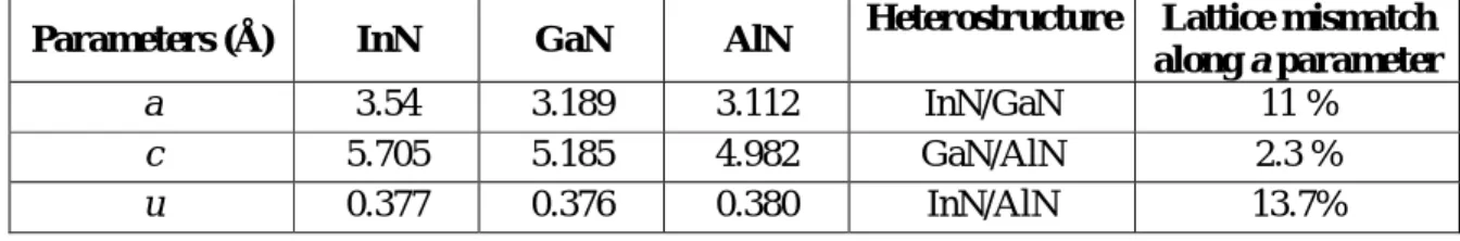
Table 1.1. Lattice parameters and lattice mismatch of bulk InN, GaN and AlN at room temperature24.
Parameters (Å) InN GaN AlN Heterostructure Lattice mismatch
along a parameter
a 3.54 3.189 3.112 InN/GaN 11 %
c 5.705 5.185 4.982 GaN/AlN 2.3 %
u 0.377 0.376 0.380 InN/AlN 13.7%
1.2.2 Crystal polarity
The group III nitrides are not centrosymmetric crystal structures, as a result, the two crystallographic directions [0001] and [0001] are not equivalent. Conventionally, the [0001] polarity is defined by the direction of the vector associated to the metal (Al/Ga/In)- nitrogen(N) bond as shown in Figure 1. 2. The epitaxial layer grown along this direction is called metal polar and the material grown in the opposite direction is called nitrogen polar. Hence the metal polar and nitrogen polar structures are the mirror images to each other. The two different polar materials possess distinct properties in terms of surface morphology, chemical reactivity, thermal stability and even the growth conditions. For instance, metal-polarity surfaces are more chemically stable than nitrogen polarity surfaces27,28.
4
Figure 1. 2. Polarity in Group III nitride: Metal polar along [0001] and Nitrogen polar along [0001]29.
The realization of the two polarities of this Group III nitride system i.e. metal polar or N-polar, is especially sensitive to the chosen substrate material and the applied growth technique as well30. The polarity of the films can be probed by various techniques like wet chemical etching, electron microscopic techniques such as Convergent Beam Electron Diffraction (CBED) patterns, Co-Axial Impact Collision Ion Scattering Spectroscopy (CAICISS) and recently hydrogen irradiation has been proposed to effectively determine the polarity27.
1.2.3 Dislocations
Dislocations are linear defects which arise from the imperfections in the crystalline structure. A material system is often prone to have dislocations irrespective of homo or hetero epitaxy. These dislocations are generated to relax the stress which arises during the growth and to decrease the global energy of the material system. These dislocations can strongly affect the device performance31,32. The origin of dislocations is the difference of lattice parameters and thermal expansion coefficients of the substrate and the epilayer. The dislocations are characterized by their Burgers vector ( ⃗) and dislocation line (⃗).
In group III nitride epitaxy, the most common dislocations are Threading Dislocations (TDs)33,34 generated at the interface of the substrate and propagating up to the surface of the layer. A dislocation can either be perfect or partial. A dislocation is said to be perfect, when its Burgers vector corresponds to an entire translation of the lattice; it is partial when the Burgers vector is a fraction of a translation of the lattice. In nitride layers grown along c, the main defects are TDs (shown in table 1.2), which forms as edge, screw or mixed type and are distinguished by the angle made between the burgers vector and the dislocation line.
5
(1) For a pure edge type dislocation, the dislocation line is perpendicular to Burgers vector ( ⃗ ). A schematic diagram of atomic planes can be used to illustrate lattice defects such as dislocations. The "extra half-plane" concept of an edge type dislocation is shown in Figure 1.3.
(2) For a screw type dislocation, the dislocation line is parallel to Burgers vector as shown in Figure 1.3.
(3) For a mixed type dislocation, there does not exist a particular well defined angular relationship between the dislocation line and the Burgers vector.
Figure 1.3. A schematic diagram showing, edge and screw dislocation35.
Table 1.2. Perfect and partial dislocations in group III nitride layers, with lines along [0001] direction32, 33.
Burger vector ( ⃗) Type of dislocation Character 1/3<1120> Edge type (a) Perfect
<0001> Screw type (c) Perfect
1/3<1123> Mixed type (a+c) Perfect
1/3<1100> Shockley partial
1/6<2023> Frank-Shockley partial
1/2<0001> Frank partial
1.2.4 Spontaneous and piezoelectric polarization
As the wurtzite structure is polar, there exists a non zero dipole moment, which gives rise to spontaneous polarization ( ⃗ ) along the polar directions. Piezoelectric polarization is generated by stress from a lattice mismatch or changes in the anion-cation bond length, which
6
changes the whole lattice structure as shown in Figure 1.4. The total polarization field inside the wurtzite crystal is the sum of spontaneous polarization and piezoelectric polarization.
Figure 1.4.(a) Spontaneous and (b) piezoelectric polarization along [0001] direction in wurtzite structure36.
The values of spontaneous polarization37,38 is presented in the table 1.3 for the three binary compounds.
Table 1.3. Spontaneous polarization for group III nitrides37,38.
Material Polarization C/m2 InN GaN AlN
Psp -0.042 -0.034 -0.090
The magnitudes of the polarization components have different values for various material combinations in heterostructures. For example, in InGaN/GaN system, the lattice mismatch increases steeply with the indium content, so that the resulting piezoelectric polarization dominates rapidly over the spontaneous polarization, whereas in AlGaN/GaN the lattice mismatch is smaller and spontaneous polarization is always dominant or at most comparable to piezoelectric polarization. These polarizations are known to affect considerably the operation of various III-nitride optoelectronic and electronic devices. However, the effects due to polarization can either be eliminated or reduced by appropriately choosing growth orientations such as non polar or semipolar directions.
7 Quantum Wells (QWs)
A QW is a thin layer which can confine carriers into two dimensions. This is obtained in semiconductors, by fabricating a heterostructure in which a material with a specific band gap is sandwiched between layers of material with a wider band gap. If this thickness of the QW is of the order of Bohr radius (3.4 nm), the energy levels inside will be quantized and their distance increased further as the well width decreases, which is known as quantum confinement energy. This quantum confinement leads to overlap of electron and hole wave functions, which in turn enhances the recombination and transition rate of these carriers. With increasing well width, the transition energy of a QW is expected to converge towards the bandgap of bulk material39. For instance in InGaN/GaN QWs, the emission energy is a function of well thickness and indium concentration. When QW structures are grown along the [0001]-direction, as the nitrides are piezoelectric material, a large strain-induced piezoelectric field is expected to be present. This internal electric field which alters the band structure of these heterostructures (shown in Figure 1.5) is called the Quantum Confined Stark Effect (QCSE).
Figure 1.5. Electronic band structure of quantum well under applied bias showing QCSE, resulting in effective bandgap narrowing and spatial separation of electron and hole wave functions40.
The primary effect of QCSE is the shift of energy levels to lower levels: the first electron level in the conduction band and the first hole level in the valence band get closer in energy. This results in a red shift of the emission41 in addition to reduction of oscillator strength42, 43. There is an adverse affect on emission efficiency due to the reduction of oscillator strength whereas this
8
strong in built internal field is advantageous in GaN/AlGaN system to fabricate high electron mobility transistors.
The other structural, electronic, thermal and optical properties of wurtzite AlN, GaN and InN are listed in Table 1. 4.
Table 1. 4. Physical properties of III nitride materials2, 3, 44, 45.
Parameter AlN GaN InN
Mass density (gcm-3) 3.23 6.15 6.81 Thermal conductivity (W/cm K) 2.85 2.06-2.1 0.8 Thermal expansion (X 10-6 K-1) ∆a/a =4.2 ∆c/c =5.3 ∆a/a =5.59 ∆c/c =3.17 ∆a/a =3 ∆c/c =4 Refractive index 2.15 ± 0.05 2.33 2.8-3.05 Dielectric constant €0 = 8.5 ± 0.2 €∞ = 4.68 - 4.84 €0 = 9.5 €∞ = 5.35 €0 = 15.3 €∞ = 8.4
Electron effective mass (me) 0.48 0.2 0.06 Electron concentration (cm-3) < 10 16 ~ 1017 1016- 1020 Electron mobility (cm2V-1S-1) 300(Theoretical) 426(Experimental) 1000(Theoretical) 900(Experimental) 4400(Theoretical) 3980(Experimental) Peak drift velocity
(X 107 cms-1) 1.7 2.9 4.2
1.3 Group III nitrides epitaxy
The common growth techniques for III nitrides are Molecular beam epitaxy (MBE), Metal organic Vapor Phase epitaxy (MOVPE), Hydride Vapor Phase epitaxy (HVPE), Sputtering and Pulsed Laser Deposition (PLD). Among them MOVPE and MBE are the most used for device processing and we have employed these techniques to grow the samples which are investigated in this work.
The quality of epitaxial layers depends upon the growth technique, the epitaxial growth mode (homoepitaxial or heteroepitaxial), the substrate used and the processing conditions. The choice of growth technique depends on the desired structure and needs, for example, in case of industrial production, MBE had less success for nitrides than MOVPE. For group III nitrides growth, although bulk GaN and AlN are available, the small size and high cost prevent their
9
wide usage. Therefore, due to the current lack of affordable bulk nitride substrates, group III nitrides are grown by heteroepitaxy. However, a number of research groups and industries are currently pioneered in the growth of bulk nitride substrates2. Lattice and thermal mismatch between epitaxial layers and substrates have long been the major challenge in obtaining high quality devices in the III-Nitride material system. The properties of the most commonly used substrates for group III nitrides are listed in Table 1.5, which indicates a large lattice and thermal mismatch between the III–nitrides and the substrates. Because of this mismatch the growth of good quality epilayers is challenging.
1.3.1 Substrates and buffer layers for group III nitrides
For epitaxial growth, one of the major issues is to select the suitable substrate.
Generally, close matched substrates are used to reduce the film stress and dislocations in epitaxial films. There are many factors which contribute to select the substrates for group III nitride epitaxy, and no single material possesses all of the desired qualities. The foremost important factors are the lattice parameters and the thermal expansion coefficients of the substrate closely match with the epitaxial film. Furthermore, the substrates must be chemically and mechanically stable at high temperatures. A substrate should be easily available in large wafer size at relatively low cost in order to make production-scale devices. A high thermal conducting substrate increases device lifetime and allows devices to operate at higher power densities. For optoelectronic purposes, the substrate should have a wide band gap and a high refractive index, so that the photons generated in the active layers of the film are not absorbed by the substrate. A number of substrates have been used for Group III nitrides epitaxy and a complete review was reported by Liu et al44.
Table 1.5. Properties of substrates for III-Nitride growth44,45,46.
Substrate Crystal symmetry
Lattice constant Å
Lattice mismatch, ∆a/a (%)
Thermal expansion coefficient
(10-6K-1)
A c GaN InN ∆a/a ∆c/c
α-Al2O3 Hexagonal 4.765 12.982 ~16 ~30 5.0 9.03
SiC Hexagonal 3.0806 15.1173 ~3.5 ~14.8 4.3 4.7
10 1.3.1.1 Sapphire substrate
Sapphire is the most extensively used substrate for growth of the III–nitrides despite of its large structural and thermal mismatch with GaN and InN (shown in Table 1.5). This is supported by the fact that the layers grown on sapphire have, in many cases, better quality and sapphire is easily available up to inches in diameter at relatively low cost. Sapphire substrates are transparent and stable at high temperatures. In general, the quality of the films grown directly (i.e., without the buffer layer) on any plane of sapphire is poor. Obtaining a good quality nitride epilayers necessitates the nitridation of sapphire substrates and an insertion of a low temperature intermediate buffer layer. Furthermore, the optical transparency of sapphire is beneficial in back-illuminated detectors and LEDs for lack of absorption. The main drawback of sapphire as a substrate, is the low thermal conductivity, which causes heat management as an important concern for high current density devices36.
1.3.1.2 Silicon carbide (SiC) substrate
Extensive work has been done on the growth of III– nitrides on SiC substrates47,48. SiC has several advantages over sapphire for InN and GaN epitaxy, which includes a smaller lattice mismatch and higher thermal conductivity. Additionally, SiC has good electrical conductivity which eases to make electrical contacts to the backside of the substrates and thereby simplifies the device structure compared to sapphire substrates. Large good quality SiC substrates are commercially available. Low temperature GaN or AlN buffer layers are also deposited on the SiC substrates before growing the nitrides. The stress developed in the films grown on SiC is smaller than that grown on sapphire, because of less lattice mismatch. SiC is also a polar material which facilitates the growth of single polar nitrides.
1.3.1.3 Silicon (Si) substrate
Generally, nitride-based devices are grown on sapphire, silicon carbide substrates. However, a considerable work has been done on the growth of group III nitrides on Si substrate. The major attractive points of Si as a substrate includes high quality, low cost, availability of large size, good electrical and thermal conductivity. In addition, Si substrate can accomplish the integration of III nitride devices with other Si based electronics. Although the crystal quality of GaN grown on Si is still poorer than that on sapphire and SiC, research on this is in great progress. A low temperature buffer layer of AlN is usually grown on Si before the growth of the main epilayer to avoid the formation of SixNy. The growth of a polar epilayer on nonpolar
11
substrate is more complicated due to the formation of additional defects, such as inversion domains.
1.4 Applications of group III nitrides
The properties of group III nitride binary compounds and alloys make them exclusive for applications in the fields of electronics and optoelectronics. The quest for these applications has
led to extensive research work on these materials from the last two decades. The re- evaluation of InN bandgap has even more broadened the spectrum of these applications.
1.4.1 Optical applications
The Solid State Lighting (SSL) technology has the potential to cut the world lighting energy usage by 20% and could contribute significantly to climate change solutions49. So the research aims at bringing LEDs solid-state lighting as the next generation of light sources for general illumination, from homes to commercial applications. In this field, research on group III nitride semiconductors is realizing breakthroughs in efficiency and performance in terms of successful launching of nitride LEDs and Laser diodes.
LED applications
Of group III (Al, Ga, In) N system, InN plays a major role in empowering the fabrication of high efficient light emitting diodes by widening the spectral region with the tuning of indium composition as shown in Figure 1.6. In other words the group III nitrides spans from near infra-
Figure 1.6. (a) Bandgap of all group III nitrides as a function of molar fraction. The solid and dashed lines are bowing curves with best-fit bowing parameters16.
1.0 0 0 2.0 3.0 4.0 5.0 6.0 7.0 350 300 400 500 600 800 AlN GaN InN InGaN infra-red visible ultra-violet 0.2 0.4 0.6 0.8 1.0 x AlGaN 250 200 b a n d g a p ( e V ) w a v e le n g th ( n m )
12
red to deep ultraviolet region. The research on nitride based LEDs was kindled by the advent of blue/green LED based on InGaN heterostructure grown on sapphire substrate50. Thereafter the research in this system was endured by red LED with indium rich InGaN heterostructures and white LEDs which have been developed by coating blue GaN LED with phosphors51.
Laser applications
The fabrication of high quality LEDs paves the way for the realization of lasers which can operate at light wavelengths from ultraviolet (UV) to green. The blue ray disc technology has replaced the traditional DVDs as the blue laser diodes can allow five times higher storage capacity. A major breakthrough in research has been accomplished by the infrared lasing in high quality single crystalline InN nanobelts52. The possibility of making ternary and quaternary nitride systems fosters the semiconductor lasers emitting from deep UV to infrared region.
Emitters and detectors
The wide band gap AlN and GaN binaries posses the potential for fabrication of UV emitters and detectors. UV emitters can be used in various applications such as material identification, forensic location, disinfection and in material processing. These III-nitride based UV detectors finds outmost usage in UV sensing applications such as automobile engine combustion sensing, high temperature flame sensing, environmental monitoring, solar blind detectors, missile plume detection for military use etc. The other most significant application of III nitride semiconductors is in the fabrication of quantum infrared detectors. Photoconductors are the most common type of quantum infrared detectors which can be realized by nitride semiconductors. The narrow band gap of InN and its alloying with GaN makes it perfect for photovoltaic applications. The InGaN ternary system can be tuned to absorb the entire visible range of solar radiation and this could result in high efficiency solar cells.
1.4.2 Electronic applications
The unique properties of InN such as small effective mass, high electron mobilities, and high peak electron velocities make InN promising for electronic devices. InN is of great interest for realization of high speed, high performance, and high frequency devices due to its inherent unique properties. InAlN can be a good candidate for high power, high temperature microwave
13
applications because of its higher breakdown voltages. InN is also ideal for terahertz applications.
1.5 Low frequency noise
The study of fluctuations in physical quantities can yield an insight into the physical phenomena, associated with fluctuations. The spontaneous fluctuations of physical quantities in the domain of electron devices are termed as noise and both terms; fluctuations and noise, are used interchangeably. For the outmost usage of the physical and chemical properties of a material, it is essential to predict the limitations of the device performances. To this end, electrical noise claims to be an accurate indicator of the quality of the materials and devices since it arises from various relaxation processes of the charge carriers, defects, or group of defects53. Noise measurement is a diagnostic tool to explore the microscopic and/or mesoscopic properties of materials under study, as noise is sensitive to transport processes; and also noise limits the smallest signal level that can be measured.
In this work, the noise measurements were of considerable interest because of primarily two reasons. Firstly, the noise as a sensitive indicator of material quality, and therefore can be used as a feedback to growers. Secondly, it provides, by comparison with theoretical models, a way to determine the dominant conduction mechanisms.
1.5.1 Noise definition
In the broadest sense, noise is any unwanted signal that comes along with the desired signal. The sources of noise can be classified into mainly two categories. The first is extrinsic noise sources which comes from interactions between the investigated system or device and the external environment which may result from electrostatic or electromagnetic coupling between the circuit and the A.C power lines or fluorescent lights, cross talk between adjacent circuits, humming from D.C. power suppliers or microphonics caused by mechanical vibration of components. Most of these disturbances can often be eliminated or minimized by adequate shielding, filtering or the layout of circuit components53. The intrinsic noise is the spontaneous fluctuations which result from the physics of devices and the materials that make up the electrical system. This noise is measured in terms of random fluctuations either in the voltage across the terminals of the device or current flowing through the device and is relative to static
14
values. The noise is randomly distributed in value and sign fluctuations are small compared to static values. From signal point of view, it can be represented as a function, b(t) which is expressed in volt for voltage fluctuations and in ampere for current fluctuations. One typical view of a noise signal is shown in Figure 1.7.
The mathematical properties of this function are the following: considering at an instant t=t0, it
can be written as
( ) = lim
→ ∫ ( ) = 0 (1.4)
and the mean square, ( ) = lim
→∞ 1
∫ + 0 ( )2
0 (1.5)
is constant at instant t0, and is constant for any t0 and depends on the physical mechanisms at the
origin of the fluctuations, the bias level and the frequency range of measurements.
Figure 1.7. A typical view of noise signal in time domain
1.5.2 Noise spectral density
The analysis of noise is more precise in the frequency domain. In the Fourier space, one can define the noise spectral density as
( ) = | [ ( )]| (1.6) where ( ) is expressed in V2/Hz for voltage fluctuations and in A2/Hz for current fluctuations. is the duration of observation of the noise and FT is the Fourier Transform.
15
Note that, should be sufficiently long, such that the mathematical statistical properties expressed before are approximately verified.
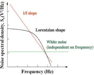
The different contributions can clearly be distinguished when one measures the noise spectral density versus frequency, which is diagrammatically represented in Figure 1. 8 in a log-log scale, where different shapes appear: 1. The white noise, where the noise spectral density is independent of the frequency; 2. Lorentzian noise which consists first in a plateau and then a decrease after a characteristic frequency fL. Several lorentzian shapes may be observed in one
noise spectrum. 3. 1/f noise with a decrease of the noise spectral density that follows a 1/f γ law. Experimental values of γ between 0.8 and 1.3 have been reported. In our case, γ value was close to 1, so it will not appear in the following.
Figure 1. 8. A diagram of the noise spectral density in log-log scale.
Considering the voltage fluctuations, the noise spectral density is expressed as the sum of the three noises, as follows:
= + + ∑
(1.7)
Where A represents the white noise level, is the 1/f noise and the parameter represents the voltage noise spectral density level at 1 Hz. The third term of the equation contributes a sum of Lorentzian components, with ai as the plateau value and fi as the characteristic frequencies.
16 1.5.3 White noise sources
There are two distinct types of white noise: thermal noise, shot noise.
Thermal noise: It is often termed as Johnson noise or white noise and is caused by the random motion of charge carriers in thermal equilibrium. In every conductor, above the absolute zero temperature, charge carriers are in random motion and this vibration is dependent on temperature.Since the motion is random, at any given time there might be a surge of charge on one side or the other leading to a voltage across the material. For a semiconductor of electrical resistance R at a temperature T, the spectral voltage noise density (Sv) is given as in equation 1.8, which shows that Sv is independent of frequency as can be seen in Figure 1. 8.
= 4 TR (1.8)
Figure 1.9. Noise representation for a physical resistor53.
Figure 1.9 represents the thermal noise model by replacing the noisy resistor with the combination of a noise-free resistor in series with a voltage-noise generator.
Shot noise: It arises from discrete carrier motion in devices. The shot noise results from the random emission of charged particles which are discrete and independent. Shot noise can be noticed in Schottky-barriers and in PN-junctions where the current results from the random motion of charged particles. The shot noise spectral density is given by,
( ) = 2 (1.9) where I is DC bias in amperes and q is elementary charge= 1.6 X 10⁻¹⁹ C.
17
Figure 1.10. Shot noise in a diode: Noise equivalent model.
1.5.4 Lorentzian noise sources
Many kind of mechanisms exists that creates lorentzian shape in the noise spectral density. First order low pass filtering of the white noise sources, popcorn or random telegraph noise for instance. In this work, we have focused on generation recombination (GR) processes of free charge carriers in a semiconductor. Such processes are related to impurities that create a trap levelstate at energy ET in the bandgap characterized by a time constant τ. In the noise spectral
density the charge carriers generation recombination at such trap level create a lorentzian shape where the characteristic frequency of the lorentzian is
πτ.
Using result from SRM model54, a relationship exists between τ and ET according to the
following equation,
( . ) =
+
∗ ∗
(1.10)
Where h: Planck’s constant, ∗: effective electron mass, ∗: effective hole mass, is Boltman constant and is capture cross section of electrons respectively. By plotting ln( . ) versus , one can obtain an Arrhenius diagram. If experimental data are well aligned, from the slope of the linear fit, the energy trap level ET can be extracted.
1.5.5 1/f noise sources
Whenever a constant voltage is applied to a resistor, a fluctuating component of the current is observed in addition to the thermal noise. Hence it is measured as excess random fluctuations
18
in the voltage when a current flows through the given resistor. The magnitude of these voltage fluctuations is proportional to the current and thus it is measured as fluctuation in the conductivity.1/f noise is also called low frequency noise because it has increasing spectral power at lower frequencies. The GR noise and 1/f noise are often termed as excess noise as they are present in addition to thermal noise and shot noise.
1.5.6 1/f noise models
It is well known that in homogeneous sample, the electrical conductivity ( ), is given by = nqμ, where q = 1.6 X 10⁻¹⁹ C, n is the free carriers concentration and μ is the free carriers mobility. The conductivity fluctuations in a material can either result from fluctuations in the number of carriers or in their mobility. Thus, 1/f current noise fluctuations can arise from either fluctuations in the number of carriers (∆N model) or fluctuations in the carrier mobility (∆μ model). Thus the voltage fluctuation spectral density, depends on either number fluctuation spectral density ( ) or mobility fluctuation spectral density ( µ), given by
= or
= µ (1.11)
where N is the total number of carriers in a homogeneous semiconductor which is related to the carrier concentration as N= n x volume, and µ is mobility of charge carriers.
In chapter 3, the quadratic dependency of versus is represented as = . . This relation is used independent of the origin of the fluctuations, where , gives the noise level at 1 Hz with a DC voltage of 1V which is applied to the resistance.
There is no universal theory for 1/f noise, however, two major competing models are available which will be briefly described in the following sections.
Mobility fluctuations
In this model, it is considered that the carriers scattering due to the lattice vibrations gives rise to the origin of 1/f noise fluctuations55,56.The mobility fluctuations are connected to the volume effect, as the fluctuations in the mobility of the carriers occur in the bulk of the material which results the observed conductivity fluctuations. By following the semi empirical formula proposed by Hooge, one can write,
19
= (1.12) Where the parameter is a constant, which is very sensitive to material quality and processing techniques. Thus, it can be used as an indicator to measure the quality and the noise level of materials and devices.
Number fluctuations
Number fluctuations are related to GR centres and as it has already been discussed, GR processes lead to Lorentzian spectrum. One condition for obtaing 1/f noise is to consider GR centres with a distribution of time constants that follows as (1/ τ) law between and . It can then be proved that for frequencies between and , the noise spectral density follows a pure 1/f noise dependency. Interface states allow obtaining such time constant distribution. It follows that number fluctuations, when observed are associated with a surface or an interface localization of 1/ f noise sources.
1.6 References
1
K. M. Yu, Z. Liliental-Weber, W. Walukiewicz, W. Shan, J. W. Ager III, S. X. Li, R. E. Jones, and E. E. Haller, H. Lu and W. J. Schaff, “On the crystalline structure, stoichiometry and band gap of InN thin films”, Appl. Phys. Lett. 86, 071910 (2005).
2
S. C. Jain, M. Willander, J. Narayan, and R. V. Overstraeten, “III-nitrides: Growth, characterization, and properties”, J. Appl. Phys. 87, 965 (2000).
3
S. N.Mohammad and H. Morkoç, “Progress and prospects of group-III nitride Semiconductors”, Prog. Quant. Electr. 20, 361 (1996).
4
F. Fichter, “Uber aluminumnitride”, Z. Anorg. Chem. 54, 322 (1907).
5
F. Fichter, and F. Schroter, Berichte der Deutschen Chemischen Gesellschaft, 43, 1465 (1910).
6
V.C.Johnson, J. B. Parsons and M. C.Crew, “Nitrogen compounds of gallium”, J. Phys. Chem. 36, 2588 (1932).
7
H. P. Maruska, J.J. Tietjen, “The preparation and properties of vapor-deposited single-crystalline GaN”, Appl. Phys. Lett. 15, 327 (1969).
8
H. M. Manasevit, F. M. Erdmann and W. I. Simpson, “Use of metalorganics preparation of semiconductor materials; IV. Nitrides of Aluminum and Gallium”. J. Electrochem. Soc. 118, 1864 (1971).
9
S. Yoshida, S. Misawa and A. Itoh, “Epitaxial growth of aluminum nitride films on sapphire by reactive evaporation ”, Appl. Phys. Lett. 26, 461 (1975).