HAL Id: tel-01278511
https://tel.archives-ouvertes.fr/tel-01278511
Submitted on 24 Feb 2016HAL is a multi-disciplinary open access archive for the deposit and dissemination of sci-entific research documents, whether they are pub-lished or not. The documents may come from teaching and research institutions in France or abroad, or from public or private research centers.
L’archive ouverte pluridisciplinaire HAL, est destinée au dépôt et à la diffusion de documents scientifiques de niveau recherche, publiés ou non, émanant des établissements d’enseignement et de recherche français ou étrangers, des laboratoires publics ou privés.
Diminution of the lithographic process variability for
advanced technology nodes
Anna Szucs
To cite this version:
Anna Szucs. Diminution of the lithographic process variability for advanced technology nodes. Micro and nanotechnologies/Microelectronics. Université Grenoble Alpes, 2015. English. �NNT : 2015GREAT129�. �tel-01278511�
THESIS
To obtain the degree of
DOCTOR FROM UNIVERSITE DE GRENOBLE
Specialty: Nano technology and Nano electronics
Ministerial Order: 6 August 2006
Presented by
Anna SZ
UCS
Directed by Cécile GOURGON and co supervised by Jonathan PLANCHOT and Maxime Besacier
Prepared at Laboratoire des Technologies de la Microélectronique (LTM) , and at STMicroelectronics, at École Doctorale d’Electronique,
Electrotechnique (EEATS)
Diminution of the lithographic
process variability for advanced
technology nodes
Thesis defended publically « 10 December 2015», In front of the jury composed of:
Mr. Peter DeBisshop
Engineer - IMEC (Reviewer)
Mr. Régis Orobtchouk
Professor assistant - INL (Reviewer)
Mr. Gérard Granet
Professor - Institut Pascal (Examiner)
Mr. Ahmad Bsiesy
Professor - LTM (President)
Mr. Jonathan PLANCHOT
Engineer - STMicroelectronics (co-supervisor)
Mme. Cécile GOURGON
Directrice de Recherches – LTM (supervisor)
Mr. Maxime BESACIER
professor assistant - LTM (co-supervisor- invited)
Mr. Jo Finders
2
THÈSE
Pour obtenir le grade de
DOCTEUR DE L’UNIVERSITÉ DE GRENOBLE
Spécialité : Nano électronique et Nano Technologies Arrêté ministériel: 7 août 2006Présentée par
Anna SZUCS
Thèse dirigée par Cécile GOURGON and Co-Encadrée par Jonathan PLANCHOT et
Maxime Besacier
Préparée au sein du Laboratoire des Technologies de la Microélectronique (LTM) et de l’entreprise STMicroelectronics à l’École Doctorale d’Electronique, Electrotechnique (EEATS)
Diminution de la variabilité du procédé
lithographique pour les nœuds
technologiques avancés
Thèse soutenue publiquement le « 10 Décembre 2015 » devant le jury composé de :
Mr. Peter DeBisshop
Ingénieur - IMEC (Rapporteur)
Mr. Régis Orobtchouk
Maître de Conférences - INL (Rapporteur)
Mr. Gérard Granet
Professeur - Institut Pascal (Examinateur)
Mr. Ahmad Bsiesy
Professeur - LTM (Président)
Mr. Jonathan PLANCHOT
Ingénieur - STMicroelectronics (Encadrant)
Mme. Cécile GOURGON
Directrice de Recherches – LTM (Directeur de thèse)
Mr. Maxime BESACIER
Maître de Conférences - LTM (encadrant - invité)
Mr. Jo Finders
3
4
Acknowledgment
I’m very grateful for all, who helped me to accomplish this work.
First of all, I would like to express my gratitude to my supervisors: Cécile Gourgon,
Maxime Besacier and Jonathan Planchot for their guidance on this project. Their
kind help, dedication and knowledge have helped to convert this thesis work from
some initial ideas to a completed thesis.
I would like to express my gratitude to all the RET (OPC) team at STMicroelectronics
for their kindness and helpful discussions. They have contributed knowledge and
friendship into my life. Beside, special thanks for this team for all the delicious cakes
during the coffee breaks – except for the little specialty from Thailand.
I would like to thank to all the members from ASML Brion, ASML, LTM, Leti and
CIME Nanotechnology who helped to complete this thesis work.
I am especially grateful to my family for their support and kind words. They have
given me endless love and support from the beginning to end, being there all the
time I needed. Also, I would like to express special thanks to Wafa and Lama for
their devoted friendship.
5
Abstract
The diminution of the lithographic process variability for advanced technology nodes
The currently used 193 nm optical lithography reaches its limits from resolution point of view. It is despite of the fact that various techniques have been developed to push this limit as much as possible. Indeed new generation lithography exists such as the EUV, but are not yet reliable to be applied in mass production. Thus in orders to maintain a robust lithographic process for these shrunk nodes, 28 nm and beyond, the optical lithography needs to be further explored. It is possible through alternatives techniques: e.g. the RETs (Resolution Enhancement Techniques), such as OPC (Optical Proximity Correction) and the double patterning. In addition to the resolution limits, advanced technology nodes are dealing with increasing complexity of design and steadily increasing process variability requiring more and more compromises.
In the light of this increasing complexity, this dissertation work is addressed to mitigate the lithographic process variability by the implementation of a correction (mitigation) flow explored mainly through the capability of computational lithography. Within this frame, our main objective is to participate to the challenge of assuring a good imaging quality for the process window limiting patterns with an acceptable gain in uDoF (usable Depth of Focus).
In order to accomplish this task, we proposed and validated a flow that might be later implemented in the production. The proposed flow consists on simulation based detection methodology of the most critical patterns that are impacted by effects coming from the mask topography and the resist profile. Furthermore it consists of the mitigation and the compensation of these effects, once the critical patterns are detected. The obtained results on the completed flow are encouraging: a validated method that detects the critical patterns and then mitigates the lithographic process variability been developed successfully.
Keywords: Microelectronics, 193 nm Optical Lithography, RET (Resolution Enhancement Techniques), OPC (Optical Proximity Correction), mask and resist 3D
6
Résumé
A l’heure actuelle, la lithographie optique 193 nm arrive à ses limites de capacité en termes de résolution des motifs dans la fenêtre du procédé souhaitée pour les nœuds avancés. Des lithographies de nouvelle génération (NGL) sont à l’étude, comme la lithographie EUV (EUV). La complexité de mise en production de ces nouvelles lithographies entraine le fait que la lithographie 193 nm continue à être exploitée pour les nœuds 28 nm et au-delà. Afin de suivre la miniaturisation le rôle des techniques alternatives comme les RET (en anglais Resolution Enhancement Techniques) tels que l’OPC (Optical Proximity Correction) est devenu primordial et essentiel. Néanmoins, la complexité croissante de design et de la variabilité du procédé lithographique font qu’il est nécessaire de faire des compromis.
Dans ce contexte de complexité croissante du procédé de fabrication, l’objectif de la thèse est de mettre en place une méthode de boucles de correction des facteurs de variabilité. Cela signifie une diminution de la variabilité des motifs complexes pour assurer une résolution suffisante dans la fenêtre de procédé. Ces motifs complexes sont très importants, car c’est eux qui peuvent diminuer la profondeur du champ commune (uDoF).
Afin d'accomplir cette tâche, nous avons proposé et validé un enchainement qui pourra être plus tard implémenté en production. L’enchainement en question consiste en une méthodologie de détection basée sur la simulation des motifs les plus critiques étant impactés par les effets issus de la topographie du masque et du profil de la résine. En outre cette méthodologie consiste en une diminution et la compensation de ces effets, une fois que ces motifs les plus critiques sont détectés. Le résultat de l’enchaînement complété sont encourageants : une méthode qui détecte et diminue les variabilités du processus lithographique pour des nœuds de technologie de 28nm a été validée. En plus elle pourrait être adaptée pour les nœuds au-delà de 28 nm.
Mots clé : Microélectronique, Lithographie optique 193 nm, RET (Resolution Enhancement Techniques), modèle OPC (Optical Proximity Correction), masque 3D, résine 3D
7
Publications
A. Szucs et al. « Best focus shift mitigation for extending the depth of focus», In: Proceedings of SPIE 8326, Optical Microlithography (2013).
A. Szucs et al. « Advanced OPC Mask-3D and Resist-3D modeling », In: Proceedings of SPIE 8326, Optical Microlithography (2014).
Co-author:
B. Le-Gratiet et al. « Patterning critical dimension control for advanced logic nodes », In: Journal
8 Table of contents Acknowledgment ...4 Abstract ...5 Résumé ...6 Publications ...7 List of acronyms ... 11 General Introduction ... 13 1 Chapter ... 16
1.1 From simple transistor to IC – CMOS technology ... 17
1.2 Fundamental concept of photolithography ... 26
1.2.1 The principle of patterning (photolithography process) ... 26
1.2.2 The Photolithography system elements ... 27
1.3 The Lithographic Performance Indicators ... 41
1.4 Resolution Enhancement Technology (RET) ... 44
1.5 Conclusion ... 46 2 Chapter ... 47 2.1 Introduction ... 48 2.2 OPC model ... 51 2.2.1 Optical model ... 51 2.2.2 Resist model ... 53
2.3 OPC model calibration ... 57
2.3.1 The basic calibration patterns ... 58
2.3.2 Process window – a reliable metrology setup ... 59
2.3.3 Modeling requirements (the accuracy rate) ... 60
2.4 Current limitations to “everything is linked” solution ... 61
2.5 Conclusion ... 63
3 Chapter ... 64
3.1 Introduction ... 65
3.2 Experimental (modeling and simulation) constraints ... 67
9
3.3.1 The motivation for a M3D model - the phase offset related the best focus deviation ... 67
3.3.2 Demonstration of the best-focus shift problematic through simulation ... 69
3.3.3 Results and discussion on the mask 3D model ... 70
3.4 Advanced 3D modeling - The Resist 3D model ... 72
3.4.1 Possible approaches of a resist 3D model construction ... 73
3.4.2 What is behind the applied resist profile aware 3D modeling? ... 75
3.5 Conclusion ... 88
4 Chapter ... 89
4.1 Detection methodology ... 90
4.2 Detection approach among the mask topography induced effects ... 90
4.2.1 The problematic among the mask topography induced effects ... 90
4.2.2 The proposed solution: mask topography conducted detector ... 90
4.2.3 Results and discussion ... 92
4.3 Detection approach among the resist profile induced effects ... 94
4.3.1 The problematic among the resist profile induced effects ... 94
4.3.2 The proposed solution: resist profile conducted detector ... 97
4.3.3 Results and discussion among the resist profile related detectors ... 98
4.4 Conclusion ... 104
5 Chapter ... 106
Introduction ... Erreur ! Signet non défini. 5.1 Mitigation of the mask topography related effects at scanner level ... 107
5.1.1 The best focus shift mitigation by wavefront optimization ... 107
5.1.2 Experimental setup for wavefront optimization ... 109
5.1.3 Results and discussion ... 112
5.1.4 Partial Conclusion on mask topography related mitigation at scanner level by wavefront optimization... 118
5.2 Mitigation through the resist profile related effects ... 119
5.2.1 The source optimization (SO) ... 120
5.2.2 Data setup for the simulation ... 122
5.2.3 Results and discussion ... 123
5.2.4 Validation of the optimized source ... 124
10 5.3 Conclusion ... 133 General conclusion ... 134 Annex 1 ... 137 6 Résumé en français ... 142 6.1 Définitions et concepts ... 143 6.2 Plan expérimental ... 146
6.3 Les résultats et les faits marquants ... 146
6.3.1 La Détection par application des modèles avancés : masque 3D / résine 3D ... 146
6.3.2 La Diminution ... 161
6.3.3 Conclusion ... 174
11
List of acronyms
AFM Atomic Force Microscope ARC Anti-Reflective Coating ArF Argon-Fluor
BARC Bottom Anti Reflective Coating CD Critical Dimension
CMOS Complementary Metal Oxide Semiconductor CMP Chemical Mechanical Planarization
DoF Depth of Focus DRC Design Rule Check DUV Deep Ultra Violet E-beam Electron Beam EL Energy Latitude EUV Extreme Ultra Violet FEM Focus Exposure Matrix
FLEX Focus Latitude enhancement Exposure IC Integrated Circuit
ITRS International Technology Roadmap for Semiconductors
LE Line End
LMC Lithography Manufacturability Check
M3D Mask 3D
MEEF Mask Enhancement Error Factor MOS Metal Oxide Semiconductor MRC Mask Rule Check
NA Numerical Aperture
NGL Next Generation Lithography OAI Off Axis Illumination
OPC Optical Proximity effects Correction OPD Optical Path Difference
OPE Optical Proximity Effect
p Pitch
PAG Photo Acid Generator
PB Post Bake
PEB Post Exposure Bake PSM Phase Shifting Mask
PW Process Window
PWQ Process Window Qualification
R Resolution
12
RET Reticle Enhancement Technology RMS Root Mean Square
SB Scatter Bar
SEM Scanning Electron Microscopy SMO Source Mask Optimization SRAF Sub Resolution Assist Feature TARC Top Anti Reflective Coating uDoF usable Depth of Focus UV Ultra Violet
Wavelength σ Partial Coherence
13
General Introduction
It has been now for at least a half century, that the microelectronic field1 is searching for pushing
its boundary with the objective to engineer more and more useful electronic devices on a given surface. The “why” sometimes is hard to understand, but the semiconductor industry is mainly driven by this fact. The currently applied Integrated Circuits’ (IC) major role is to implement as much electronic function as possible with various complexity levels on the same chip. Then, these IC are used in a large scope of applications from entertainment industry to military applications. Indeed to satisfy these various needs, related to semiconductor industry, any perspective progresses towards the improvement of such electronic systems.
The major conducting parameters in research, with the objective to achieve higher performance ICs, are the speed, the integration density, the reduced consumption of power and, of course, the reduced fabrication costs. Linked to the cost reduction, a pronounced effort needs to be put on the capability and robustness of the process.
Focusing on the complex processing stages of IC’s mass-production, without boasting, we can say that its centerpiece is the lithography. It is coming from the fact that the IC’s speed and the component’s integration density depend on the minimum feature size or critical dimension (CD) that can be resulted by the lithography. Indeed, the higher integration density on a given surface enables the circuit a higher complexity level. It is coupled with higher velocity for similar fabrication costs. Beyond this aspect, the lithography accounts around 30 % of the total manufacturing costs of a chip (Mack C. , 2015). This percentage is unceasingly increasing and is one of the most critical point for the process.
As current state in mass production, the mostly applied technology is the photolithography that enables an efficient compromise in between robustness and high productivity capability. It uses deep ultraviolet monochromatic (DUV) light to rapidly pattern all the design of the transistor. It is realized by transferring the object, the photomask image, into the photo sensible material (photoresist) on a substrate through a projection system. Its exposure wavelength and numerical aperture (NA) are directly related to the minimum feature size – thus the resolution limit. The decrease of the exposure wavelength or the augmentation of the NA would enable to minimize the smallest dimension that can be patterned. Currently the most reliable photolithography tool in industry for advanced nodes (28nm) in term of capability, robustness is the projection system with 193 nm of exposure wavelength and 1.35 NA. Several techniques were tested in the beginning of this century to decrease the wavelength: as example 157 nm aiming the 65 nm node technology or 126 nm aiming the 45 nm node technology. Nevertheless there was no success due to the uncontrollable illumination source of the tool and due to difficulties in the projection optics (lens). Thus the 193 nm projection systems seemed to be the best choice that required further enhancement, as it was initially intended to use for 90 and 65 nm nodes technologies and not for “28 nm and beyond”.
1 The microelectronic field encompass: the study and the fabrication of electronic components at the micro and nano
14
Indeed, there is a physical limit, but still the resolution limit is pushed as far as possible. It means that the lithographers are faced to this challenge to figure out new imaging strategies (and tool enhancement). The ensemble of the various original ideas and the creativity, usually referred as Resolution Enhancement Techniques (RETs), temporarily offers solution to push the limiting factors of the projection printing. Thus it is still possible to follow the miniaturization tendency by the support of RETs, including e.g. Optical Proximity Correction (OPC) to compensate the process induced effects by modifying the sizes and the shapes of patterns at mask level.
The processing solutions for 28 nm and beyond nodes would not be possible in fact without these knobs. In addition to the shrunk dimension, these advanced nodes have to deal with complex features at design level, such as metal layers. The resolution within a sufficient process window is in fact a challenge. The process window means the range of tolerated variation of the position of the focal plane and the dose for which the resolution is within a specified limit. It is usually referred by the usable Depth of Focus (uDoF) – the higher uDoF is, the more stable the process is. So, the aim is to expand as much as possible the uDoF, since for 28 nm and beyond nodes the uDoF is now indeed reduced.
The thesis work then is put in this increasingly complex production environment with the objective to establish a process variability correction methodology that would enable for these complex patterns an expanded process window. In order to achieve this set goal, it is first necessary to detect and select the most critical features by an efficient methodology supported by computational lithography. Then the process variability needs to be mitigated through these detected patterns. The thesis work layout is as follow:
The first chapter describes in details the context. A brief history and substances on the semiconductor industry are presented for a deeper understanding of important aspects of integrated circuits (ICs) fabrication and its challenge faced to engineering. The emphasis is then put on the photolithography by the description of a classical exposure system. Its boundaries are listed as well as a possible way of amelioration for each of them - outlined of the importance of the computational lithography (thus OPC modeling).
The second chapter deals with the State-of-Art focusing on the interrelation of OPC modeling and production environment. For deeper understanding of the challenge hide behind, a description is provided on the modeling portion of the scanner. Then from the current limitations we arrive to an “everything is linked”. It means that we anticipate in the realization of a dynamic link between OPC and process environment by the setup of our above mentioned correction methodology.
The third chapter is dedicated to ground of the detection part by the enhancement of the available OPC models’ upfront prediction. The necessity is coming from the fact that the conventional models became obsolete for shrunk nodes. In the light of this fact, the intention is put on the introduction of the construction background of 3D aware modeling (mask 3D and resist 3D) enabling an efficient support for a higher level detection of critical features.
The forth chapter is dedicated subsequently to the detection and selection of the most critical patterns based on the calibrated 3D aware OPC models. It includes discussions from the basic
15
consideration to the proof of concept. The detection and selection is conducted among the mask topography related and the resist profile related effects. Our objective is to validate the set detection methodologies as efficient and reliable support for production on design layout.
Finally, the fifth chapter provides the mitigation solution of the process variation on the previously detected critical patterns in continuity of the forth chapter. Subsequent to the forth chapter, two approaches are demonstrated, one for compensation of the mask topography effects and one for the resist profile effects.
16
1
Chapter
Introduction to the photolithography
The apace developing and shrinking micro components of a circuit board are followed by a steadily increasing complexity of process. Behind this engineering feat, the machinery needs to respond to this high complexity task. Current IC (Integrated Circuit) process technology owns fabrication processes consisting of hundreds process steps applied on a raw semiconductor material wafer. The majority of these steps can be aggregated into the following ensembles:
- Photo mask pattern transfer by lithography and etching - Layer forming by deposition, oxidation or metallization - Modification of the layer by ion implantation and diffusion.
The lithography is one of the essential processes in the fabrication plant that can be called also the heart of the micro component technology. Its main task is to transfer the designed photomask pattern image on the silicon wafer surface. This patterning method had and has an efficient adaptive capability to support different technologies from 10 µm technology nodes from early stage of IC fabrication (1960) to today’s 28 nm and beyond. Therefor the extension of lithography limits is steadily on-going, which is driven by transistor dimension shrinking.
So this requirement provided the bedrock of this thesis work that is placed into the lithography world. Thus this chapter is dedicated first to a brief historical insight in the semiconductor industry from the invention of the first transistor to current challenges (through the elementary MOS transistor). More precisely, at this point, we will investigate in the basic concept of lithography, more specifically of the photolithography. This part will include a description of a classical exposure system emphasizing on its characteristics, performance indicators, but also limitation factors and possible improvement.
17
1.1
From simple transistor to IC – CMOS technology
As foreword of this thesis work, the main entrances to the microelectronic world is the concept of the first bipolar-junction transistor on a germanium monocrystalline by the team of W. B. Shockley dated at 1949. A transistor is a semiconductor component or device that can be used to switch or to amplify electronic signals and power.
The concept of the first transistor is a result of an initialized research project on semiconductor technology to replace vacuum tubes for telephone applications. This investigation was started because of the weak reliability and pronounced power consumption of vacuum tubes used for phones. Their ability could not follow the increasing phone call capacity. The patent of the junction transistor is the result of W. B. Shockley‘s theoretical activity on the point-contact transistor, an early transistor solution by Bardeen and Brattain. Besides the deeper understanding of his theoretical work, the junction transistor showed more potential to be a good candidate for high volume production.
Five years later from its first introduction, as the initial stage of the electrical micro component fabrication, the transistor commercialization has been already started in the same Bell Laboratories. For many years, transistors were fabricated as individual components and the connection between these electronic components (diodes, capacitors, etc.) was realized on a board to obtain an electronic circuit (circuit board). The need of a smaller, faster circuit board came with the fact that there was a pronounced issue due to time delays for electrical signals to propagate on such a long distance in these wildish boards. Thus after many developments J. Kilby from Texas Instruments came up with the solution to this problematic of a multitude of components. So the first integrated circuit (IC) was built, placing several transistors, in additional some diodes and resistors, by the same process on the same semiconductor surface.
In 1968 the team of R. Noyce put down the technology enabling the IC realization of the MOS (Metal Oxide Semiconductor) transistors. Different MOS transistors, with different conductions – N and P type – enabled the construction of logic functions. The technology making use of both P and N channel devices within the same substrate material, so called CMOS (Complementary Metal
Oxide Semiconductors) technology, is then the milestone of industrial IC development. Until
present-day solutions, this CMOS processing technology is the most currently applied in the integrated circuit industry. This technology method’s flexibility allows an efficient adaptation to a large scale of existing and innovative applications. It is still a key solution for the current global trend realizing electronic components with a better tradeoff between energy consumption and performance (Zeggaoui, 2011) (Michel J.-C. , 2014) (CHM, 2015) (Wikipedia, 2015).
The following sections are dedicated to the description of the basic mechanism of MOS transistor. The basic elements of an Integrated Circuit – MOS transistor and its operation
1.1.1
The basic element of an electronic gadget or an IC is the MOS (Metal Oxide Semiconductor) transistor. It is composed of three electrode terminals: Gate, Source and Drain. The illustrated example, a MOS transistor, on Figure 1, is “processed” on bulk silicon substrate and consists on the following principal elements:
18
- Substrate : silicon substrate doped N (N type transistor) or P ( P type transistor);
- Gate : commanding electrode of the transistor that can be poly-silicon or a stack of metal gate for advanced technologies; noted by number 3 on Figure 1
- Source/Drain : corresponding to a highly doped charge tank with an opposite doping type to the substrate’s – indicated by number 5 and 6 respectively Source and Drain on Figure 1; - Insulating dielectric layer: usually SiO2,or for advanced application, it can be a high K
dielectric in additional on SiO2 – indicated as number 4. Gate oxide on Figure 1;
- Shallow Trench Isolation (STI): applied to electrically isolate transistors in between each other - represented by number 2 on Figure 1.
Figure 1 Simplified cross section and 3D view of a MOS transistor with its basic elements
A key point to note is that a technology node in fabrication is denoted (most usually) by the dimension of the Gate as marked “L” on Figure 1. Mostly the shorter size of the Gate is called Gate Length “L” and the longer is called Gate Width “W
This MOS device is voltage controlled. By means that it is analogous to an electrical switch and enables the passage of the electric current according to the applied voltage on the gate. The operational principle is based on the ‘field effect’, on the electrostatic modulation of the density of mobile charges in the semiconductor. It can be occurred either by a potential variation between the Gate and the Source (VGS) that creates inversion charges at the surface of the semiconductor by
a transversal field effect through the Gate Oxide. Or either a potential difference among the Source and the Drain (VDS) that enables the circulation of the minority carriers between them that
generates the Drain Current (ID) (Rahhal, 2014). Figure 2 represents the named Field effect on a
MOS stack. Usually it is called MOSFET refering to Metal Oxide Semiconductor Field Effect Transistor.
19
(a) (b)
Figure 2 Representation of the Field effect for a MOS transistor (a) VGS=0 [V] so no channel is induced therefor
IDS=0 [A] (b) VGS > 0 [V] channel is filled with minority carriers thus IDS ≠0 [A]
Now, if the applied VGS is lower than the threshold voltage (VTh), the transistor remains blocked or
non-conducting. This means that there is no circulating current between the Source and the Drain. Still if VGS is equivalent or higher than VTh, the involved minority carriers are vertically modulated
to the semiconductor’s surface thus a channel region is obtained under the Gate’s insulator, the Tox. If the minor carrier’s modulation is realized vertically by applied VDS, an IDS current will pass
from the Drain to the Source (see Figure 3).
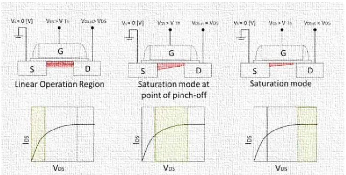
The simplified representation of the MOS transistor’s different Operating Regimes in function of the applied VDS is represented on Figure 3. Three regions are differentiated (from left to right on Figure 3):
− The linear Operation Region, where the VDS is negligible, thus IDS shows linear tendency in
function of the increasing VDS ;
− The Saturation mode at point of pinch-off, where the applied VDS is equal to the VDSaturation ;
− The Saturation mode , where the applied VDS is higher than the VDSaturation (the VDS is a
pronounce value), thus the device is controlled by the VDS and the IDS is constant
Note: for further details, the reader is kindly invited to check the following references (Arfaoui, 2012) (Rahhal, 2014).
20
Figure 3 the MOS transistor’s different Operating Regimes in function of the applied VDS:
The proper functioning of a complex electronic circuit, based on these elementary adobes, has well defined requirements that need an optimal operation of the transistor components. As example to obtain a transistor with low consumption, the output or Drain current (ION or IDS) needs to be the
highest possible with a low level of the leakage current (IOFF or IGS). Note: the IOFF leakage current
is when the channel is blocked and the ION Drain current is appearing when the transistor is in a
passing mode of operation, when the channel is induced:
- The leakage current, IOFF , is obtained while � = 0 [ ] and � = [ ] (NMOS) and
� = − [V] (PMOS)
- The Drain current, ION , is obtained while � = � = (����) ; � = � =
( ���)
IOFF and ION can be calculated as follow:
�=� �(���−��ℎ) , where �=����
Equation 1
W: Channel width [µm] L: Channel length [µm] µ: minor carrier’s mobility Tox: Dielectric thickness [µm]
ox: Permittivity of dielectric
Cox: Dielectric capacity
VG: Gate voltage [V]
21
These current parameters, ION and IOFF , then are usually applied as a good performance indicator
of such a device. IOFF indicates the leakage level of the transistor, thus the static consumption.
Besides, ION reveals in the operational velocity and speed. Thus a high ION/IOFF ratio is better for a
device. Overall, an ideal transistor needs to have an IOFF as low as possible, an ION as pronounced
as possible with a more abrupt possible transition between them.
The objective of the mainstream production is always making compromises, so a real end product cannot meet these “ideal” criteria. Depending on the final functional application, the priority of the operational velocity and power can be less determinative. Thus the following groups can be distinguished related to the operation specifications:
- HP = High Performance transistors : high speed, but with relatively high leakage current ; high IOFF and ION (e.g. microprocessors)
- LP = Low Power transistor : less power consumption , but higher saturation current ; low IOFF and ION (cell phones, media players)
- GP = General purpose transistors: these types of transistors are a compromise in between high speed and less consumption.
The CMOS Integrated circuit 1.1.2
A complex CMOS Integrated Circuit includes a large scale of NMOS and PMOS transistor couples built as blocks on a wafer. The purpose is the realization of logical operations (based on OR, XOR, AND, NAND… circuits connection solutions (Babaud, 2010)). From process point of view, an IC block can be divided into the two main parts, which are the following (figure 4):
- FEOL (Front End Of Line) – situated closer to the wafer surface and consisting of all the main layers defining the transistor, also called active part
- BEOL (Back End Of Line) – including all the metal interconnection layers that enable to supply or to control the active part of the circuit
22 From data sheet to IC
1.1.3
Due to these complex requirements for the fabrication of the transistors, the process in integrity needs to be well composed from the very first step following the predefined need. The first stage of this sequence is the definition of the electric schema so called “design” followed by the data sheet or also called specifications. The design will meet with the final application need on a chip, the rectangular area containing the complete IC design. It will also define the transistor’s exact positioning within. Once the electrical pre-simulations are accomplished the complete design is transliterated on the substrate wafer. It is enabled by a given number of insulator, metal and semiconductor layers. Each of these layers is represented on a design level by corresponding geometrical polygons. In order to maintain the operational requirements, design rules are applied focusing on these polygons. Basically it means a series of parameters that characterize certain geometric and connectivity restrictions ensuring the good functionality of the designed device (See Figure 5). Besides it has to ensure an adequate margin of the process variability so that each component works well.
Figure 5 Simplified illustration of design rule
Note that each technology node has its fixed design rules, specific to each layer. It is important to accomplish these rules as they are the bedrock of the transistor’s proper functioning.
The miniaturization and its impact 1.1.4
From the early development stage on transistors until present-day innovation, the main barrier imposed to semiconductor engineers is the dimension shrinking, the miniaturization. Smaller is better in the sense that the major goal is to obtain higher transistor density on raw silicon wafer maintaining the advantageous properties (or even better performance regarding the speed and the consumption as example) in addition to the application and functional implication. Figure 6 illustrates the problematic of shrinking dimensions: it shows how a shrink of the dimensions by a
23
Figure 6 Illustration of the dimension scaling “smaller is the better law” (Colidre, 2014) indicating the parameter changing in case of a shrink by α factor
The maintenance of the proper functioning at this high complexity level requires a well composed integration and information manipulation. It includes a large scale of electronic components; therefor the compilation has to be without any degradation. This needs to settle on highly reliable transistors (as example). It has to be mentioned that by this apace miniaturization of MOS transistors, new physical barriers and new parasitic effects appeared. These effects might degrade the component’s functioning such as the short channel effects, the depletion of the grid, parasitic resistances or other gate control loss related phenomena in the channel (Colidre, 2014).
The process fabrication sequence 1.1.5
In order to follow the above mentioned, steadily decreasing dimension tendency, all the machinery behind the scene has to ensure a well-controlled, robust process. The current IC process technology consists on numerous process steps applied on a wafer. The worldwide applied semiconductor material for the substrate is the silicon monocrystalline. Indeed new solutions are in progress. As industrial consideration and knowing-how, the size of the wafer is increasing in parallel with the chip size shrinking. It means that the wafer dimension became six times larger than the first generation product from 1970’s. Present-day factories capability reaches the 300 nm diameter, but the 450 mm is already under thinking. It is important from the processed chip number point of view, thus from the productivity effectiveness.
24
A fully processed chip requires several hundreds of process steps synchronized by the process integration – optimization of process step sequence combination in an economic way. The Figure 7 illustrates the simplified schema arriving to an operational transistor.
Figure 7 Schema representing the main process step
Starting from a single crystal silicon wafer it is pattern using repetitive process steps such as lithographic, deposition, diffusion and etching steps as far as a functional IC is built. A set of about thirty separate wafer processing cycles, forming modules, are accomplished. Obviously the number of these cycles depends on the technology complexity. The figure 8 shows a simplified IC fabrication cycles flow chart including the following sequences/stages:
- Layer forming consisting of a film/layer deposition on top of the material: Deposition of a material on top of another material;
Epitaxial growing of the crystal of a material on another material; Metallization ;
- Photo mask pattern transfer:
Photolithography : it consists on the designed photomask pattern image transfer on the photoresist coated wafer;
Etching : it consists on etching out the undesired resist and consists of transferring the designed pattern image (negative) into the substrate;
- Modification of the layer
Ion implantation/Doping: it consists on the chemical introduction of an element into the material;
- Chemical Mechanical Polishing (CMP): it consists on flatting the surface of the material; - Cleaning consisting on the removal of residual material;
- Electrical test/Optical inspection: each process steps are assisted by metrology for verification purpose as follow:
In-line characterization by Scanning Electron Microscope (SEM) Defectivity analysis
Electrical tests
25
It indicates the entering wafer (silicon substrate) in the fab that will go through the shown sequence’s stages until it arrives after inspection.
Figure 8 Simplified process sequence flow chart of IC fabrication
Within this flow chart, the lithography can be considered as the heart of the process. It is due to the fact that the lithography step defines the dimension of the fabricated patterns. The thesis work is situated within this critical domain of photolithography. Note that a variety of possible patterning technologies exist, but the best compromise in term of throughput and favorable defectivity in semiconductor manufacturing is still the photolithography. Other patterning solutions are not discussed here.
26
1.2
Fundamental concept of photolithography
The photolithography is defined by the creation of patterns within a layer of photoresist that covers the silicon wafer. The patterns are then transferred into the substrate by etching or ion implantation.
Thereby the precision and the control of this process step is a major task following the shrinking dimensions. The capability scale of the printing can be measured from a few microns to submicron’s current state around nm by applying a wavelength of nm, nm, nm or 193 nm. The current critical dimension (CD) that can be realized by DUV (Deep Ultra Violet) projection with 193nm wavelength is 32 nm that follows the lithography requirements from the International Technology Roadmap for Semiconductors (ITRS). Note that basically the ITRS is designated to ensure an economic advancement in the performance of integrated circuits and the product that apply them (ITRS, 2014). Within this section the basic conception of the photolithography itself and its machinery will be described.
1.2.1 The principle of patterning (photolithography process)
The photolithography process, or so called the patterning, operational principle is based on the resist aptness to store an image of the pattern to be replicated/printed. The basic operation behind such an apparatus are shown on Figure 9 indicating the system elements.
Figure 9 Principle of optical lithography - Note: figure not in scale
As initial point, the illumination system is represented, which main function is to modify the resist dissolution rate. Then the light will reach the Photomask that is composed of a large set of patterns. The light is basically transmitted only through the transparent region. As the mask is partially transparent, it creates an indirect optical source. Its objective is to modify locally the
27
energy into the photoresist. Therefor the layout pattern is then replicated onto the photoresist coated wafer. The optical system, composed by a set of lens, enables the image transfer by reducing the mask image. The resist coated wafer is placed in the image plane in order to be exposed by the incoming light from the optical system. In general the intensity of the light impinging on top of the resist is named the aerial image. Thus the pattern now is stored as latent images2 within until the wafer is put into a developer solution. During the development, the
exposed areas, depending on the resist polarity, remain or dissolve, completing the lithography process. Finally the opening areas in the resist are formed and are ready for subsequent processing: etching or implantation.
1.2.2 The Photolithography system elements
Under the term of photolithography, a projection printing tool is referred to a scanner system or a step-and-repeat (reduction stepper) system. The scanning projection printing systems, the earlier machinery, use reflective optics (mirrors) to transmit the light from the photomask onto the photoresist coated wafer, while the wafers are moved in the same moment by the slit. This scanner’s magnification is M=1. The step-and-repeat (so called stepper / figure 10) systems expose the coated wafer with a rectangular area, an image field, at a time. The magnification can vary typically from M=1 to M=1/5. Reflective systems/lenses are employed within these complex machineries.
Figure 10 Illustration of (left) a scanner and of (right) a step-and-repeat concept
Hereafter hybrid approaches appeared such the step-and-scan that became dominant. It uses a fraction of a standard stepper field then it scans the field in one direction. These tools are designed to meet a high volume production with a high resolution capability, thus their application is frequent in fab. Note that in the framework of this thesis work, a step-and-scan tool was put into focus (Twinscan®)
28 1.2.2.1 The subsystems of a photolithographic tool
The sub-systems of a projection printing system (figure 11) comprise: - An illumination system;
- A photomask;
- A projection optics/lens.
Figure 11 a projection printing system indicating the location of each sub-system that will be described later in this chapter 1
Figure 12 shows a simplified schema of the imaging theory behind such a tool. The image formation is referred to Abbé imaging theory (1872): the plane waves from a light source are diffracted by the reticle (object). Then they are recombined by the projection lens. The lens focuses the incident light from infinity to the Focal point. The diffraction pattern functions as a light source and it propagates to the image plane where it is formed (Cambridge, 2014).
29
Figure 12: Representation of the image formation based on the Abbé theory
1.2.2.1.1 The illumination system
The first sub system of a lithographic tool, from incident light point view is the illumination system (see Figure 11). It is configured to supply a projection beam of radiation that consists of the combination of light source and condenser lens.
1.2.2.1.1.1 The light source
For the light source in lithography equipment, monochromatic3 light is used. The coupled
wavelengths are ranging within the ultraviolet UV , deep-ultraviolet (DUV) and extreme ultraviolet domain (EUV). The decrease of the exposure wavelength is needed to follow the shrinking device dimensions demands. Therefor the supply of the projection beam of radiation with a mitigated needs a light source that can maintain the robustness for this change EUV supply systems are not at this point yet). As current state, in mainstream manufacturing and development, the more stable embodiment is the excimer laser light source (Figure 13). The excimer lasers are pulsed discharge gas lasers providing light output in the UV region of the spectrum. The term of “laser” is an acronym for: Light Amplification by Stimulated Emission of Radiation (Stanley Wolf, 2004). While the “excimer” is referred to the excited dimer4, molecules
that exist only in this excited state.
3 Monochromaticity: ~ refers to the single frequency / wavelength property of the radiation. A monochromatic laser
radiation has its origin in the stimulated emission process that supports the laser to emit light.
30
Figure 13 Light source module schematic view showing the excimer laser (the “invisible” part of a scanner built under the tool in the basement)
The excimer laser applies a combination of a noble gas and a reactive gas. Under specific conditions of high pressure and electrical stimulation an excimer is created, that exists only in this excited state. The excited state is a short period of time and is not stable. The forming excimer molecule corresponds to optical amplification needed to initiate a laser action (Maini, 2013). Note that in most current applications, the Argon Fluoride (ArF) excimer laser is employed to emit
= nm DUV light.
In order to enable and to ensure an adequate lighting uniformity on the photomask, the most common applied illumination systems is configured with Köhler illumination using condenser (see Figure 14).
31
The implied method means that all the subsystems are positioned in a way that the light source coincides with the focal plane of the converging lens, the condenser5. Thus this method has an
important property: the rays from each source point illuminate the photomask as a parallel beam. Therefor the reticle benefits of the same amount of lighting or illumination energy. Further, this arrangement enables that irregularities in the source brightness distribution will not result in any disadvantageous irregularities in the intensity of the object (mask) illumination.
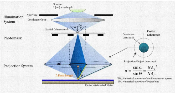
1.2.2.1.1.2 The coherence or the fill factor of the illumination
In addition to this adequate across-field dose uniformity, the directional uniformity has to be insured so that the same patterns are replicated identically. The illumination is characterized by the coherence6, or fill factor has two important aspects. First, due to the assumption of the light
source monochromaticity, in the time domain the light is considered strongly coherent. In spite of that, in the spatial domain, the coherence becomes variable (measure of the physical extent of the light source, its radius) having a pronounced influence capability on imaging performance. The spatial coherence in projection apparatus is defined as the light phase relationship as it propagates from the illuminator system towards the photomask. For tight numerical aperture (NA) in the illuminator system, no angular distribution to the illumination, there is no distribution of the light phase. Thus this can be considered as spatially coherent or a point source. In spite of that increased numerical aperture in the illuminator lead to increased angular distribution of the illumination towards the photomask. Then the illumination is called partial coherent. The aspect of “partial” is referring to occurrence of a certain amount of spatial coherence. In the limit of an infinite (or maximum NA), where all the possible illumination angles are present at mask level, the imaging is spatial incoherent. Note that the NA reveals in the ability of the lens to collect light. As shown on Figure 15, the level of the spatial coherence is quantified by the ratio of the illuminator system NA, the condenser NAC to the projection lens NAP. It is called partial coherence
factor or sigma σ and is calculated as following (Eq2):
� = �� Ɵ �� � =�� ��
Equation 2
The magnitude of the partial coherence varies between 0 and 1 as follow: - σ = : spatial coherent illumination or point source ;
- < σ< : partially coherent illumination ; - σ = : incoherent illumination.
5 Condenser lens: converging lens in the illumination system that consists of a large set of lenses, filters, mirrors and
additional optical elements.
6 Coherence : the phase relationship of light at two different points in space at any instant in time (Mack C. A., 2006); a
32
Figure 15 : Projection imaging apparatus simplified schema on optical elements (the Illumination system, the Photomask and the Projection System) with Köhler illumination indicating the image of the condenser in the
object lens
Further improvement on the illumination system, in respect to the coherence, can be obtained by the application of an aperture between the light source and the condenser lens. It will function as a wavefront filter. The shapes of the additional aperture are typically circular, annular or quadripolar. A circular element reveals then a low pass filter. Meanwhile an annular or a quadripolar element’s main function is to block the vertical or zero-order waves (without carried information). In current optical lithography towards sub-wavelength resolution such modified configurations with off-axis illumination are applied. More detailed description will be given in the context of resolution enhancement techniques within chapter1.
1.2.2.1.2 The Photomask
The next subsystem of a lithographic apparatus is the photomask on which the patterns are defined. It has an important rule, because these patterns are the structures that are replicated. Thus the final product quality can be considered as direct dependent on the photomask. The mask quality is mainly based on the mask set components, dimensions, flatness, mask shop precision and the defectivity. Beside, as all elements of the lithography tool, it should correspond to the demand for high-resolution.
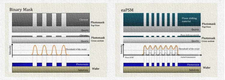
As shown on Figure 16, the simplest mask type is the binary (or COG = Chrome on Glass). It consists on a substrate made of an “exposure-wavelength transparent” material. The patterns are etched into the chrome layer whose thickness is a few nanometers that behaves as an absorber at this wavelength. The term of binary comes from the fact that it has a transparent and an absorbent region. The central limit of this type of mask is related to the opaque pattern. It means that pattern
33
with critical dimension lower than the exposure wavelength produces incorrect patterns at wafer level due to interferences and diffraction. Binary masks are usually applicable up to 0.18 µm technology nodes. Advanced binary mask are Opaque MoSi on Glass (OMOG) that result in better CD performance and in higher resolution. These materials are applied in this thesis work.
Beside the standard binary intensity masks, there are large scales of other types of photomask concepts that enhance the optical resolution for shrunk dimension technology nodes. These types include the alternating phase-shift, attenuated phase-shift (PSM) as well as assorted hybrid types. These mask technologies are applied for line width lower than the exposure wavelength. As current state, the mostly implemented concept in addition to the OMOG is the attenuated PSM. Figure 16 represents basics of these mask concepts by illustrating a top and cross-sectional view of each with the corresponding intensity (indicating the resulting Sum Intensity by yellow color).
Figure 16: Representation of the Binary vs eaPSM photomask [Toppan] illustrating the comparison of the obtained light intensity at wafer level.
The Attenuated PSM consists on a chrome layer and a semitransparent layer that shifts the phase angle of the light compared to light passing through the opening area of the photomask. The passing light’s speed is altering, through the material shifting, its phase angle. Thus this kind of material is so called phase shifting material or semitransparent material. Therefore the phase shifting mask is changing the transmitted light, the intensity distribution and as well as it varies the transmitted light’s phase at some region of the mask (Figure 16, Figure 17).
34
Figure 17: Simplified (not in scale!) schema of the Phase shift through a phase shifting material (Laube, 2014)
The Phase Shifting material thickness is determined to obtain the phase shift of 180 degree. For advanced nodes, the Electromagnetic Field effect needs to be taken into account (Laube, 2014). It requires the mitigation of the thickness that is challenging for PSM masks, as it impacts the phase shifting. The solution for that problematic is either the application of the OMOG (as it is in the case in this thesis work) or the application of an eaPSM using an optimized absorber.
1.2.2.1.3 The projection optics
The projection optics is composed in a way that the lens system enables to collect the incoming light. It means a part of the diffracted orders at mask level are participating to image formation at wafer level. Then it enables to project it further on the wafer (image plane). Thus the reconstitution of the pattern image (from the mask) is realized by the phenomenon of interference of the collected waves in the photoresist. The aerial image designates the light intensity formed at wafer level in the air, or in the immersion liquid in case of immersion photolithography. In general a projection optic system is characterized by the value of its magnification and the NA. As earlier mentioned, the magnification (M) is referring to the reduction factor in between the mask pattern dimension and the obtained pattern dimension on wafer. The numerical aperture defines the maximum angle that makes a light beam diffracted and then captured by the projection optic. Further improvement is possible to increase the magnitude of the numerical aperture, as it is limited by the lens geometry (diameter, curvature). One of a widely applied key to improve is an immersion liquid inserted in between the exit of the projection optic and the wafer stage (see Figure 18 . The inserted liquid enables an increase of the NA: whereas in dry optics NA = sin , in
35
immersed optic NA = n sin , where n is the refractive index of the liquid. Thus in case of water as immersion liquid it results in an increase factor 1.44.
Figure 18 : Simplified schema on dry optics vs. immersion optics
Note that the other aspect of the way of improvement is related to the optical aberration7 and the
lens quality that will be more detailed in Chapter 5 (FlexWave). 1.2.2.2 The formation of the aerial image
The incident light passing through the mask is diffracted at different directions and angles. The interactions of the diffracted orders captured by the projection pupils form the image of the mask pattern that is projected onto the photoresist. It is so called aerial image. The goal is to create a high-fidelity image compared to the mask pattern.
The diffraction provides the Fourier transform of the mask. The imaging limitation is coming from the fact that the projection lenses have finite size. Even if they are constructed to behave so as they could result in inverse Fourier transform of the diffraction pattern creating the “ideal” image of the mask, this finite size of the NA limits spatially the incoming diffracted orders. Thus only a certain amount of diffracted orders are participating to image formation (see Figure 19).
7 Aberration : ~ is any divergence from the ideal « diffraction limited » imaging performance of a given lens (Mack C.
36
Figure 19 : Simplified schema illustrating the diffracted phenomena on a (periodic) line vs. pitch configured structure: (a) diffracted orders distribution under coherent illumination by indicating the filtering behavior of
the exit pupil (b) diffracted orders distribution under partially coherent illumination
Due to the diffraction limited behavior of an optical system, there is loss in term of mask pattern information related to the captured (or non-captured) diffracted orders, as well as there is a relatively high light intensity loss compared to an ideal imaging case. Despite of the degradation, the capture of first diffracted orders is sufficient enough to form an image.
In order to calculate the diffracted light direction, a simple example is taken (see
Figure 19 (a)) with a monochromatic coherent radiation that arrives on a periodic line vs. pitch structured mask. The direction sin(� ) is defined by the Bragg’s law (Landis, 2011) as follow:
�� (� ) = ∗ � ; = 0, ±1 ± ,2, …
Equation 3
Where m is the diffraction angle, m is an integer indicating the diffraction orders , is the
wavelength of the exposure and p defines the pitch or period of the structure on mask (see
Figure 19). As pattern dimensions and so pattern pitches mitigate, it would impose an increased angle of diffracted orders. It also means that fewer diffracted orders are captured by the imaging system, the optical system. Thus it leads to provide an image with less frequency details, resulting in degradation on the resolution capability. The limitation of the image quality is then defined by a minimum pitch associated with the “feasibility” of at least one interaction in between two diffracted orders.
Let consider a partially coherent illumination with a conventional source σ as example. Each scattered, incoming plane wave is referred as a diffracted order. The diffracted orders distribution
37
behavior for each point is identical to the simple previously described coherent case and calculated as follow:
�� � = � ∗ ��
Equation 4
Where ϕ is the light beam angle, σ is the radius of the diffracted order at pupil level and NA is the numerical aperture. Identical to the previous case, minimum the two first diffracted orders are required for imaging (image formation) at the image plane, and at wafer level by the phenomena of interference. Based on source behaving properties (Zeggaoui, 2011), an interference occurs between two beams if they are coupled from the same initial point. For each captured diffracted order in the projection lens, each captured point interacts with its counterpart from the identical point source. Therefor the interactions can occur between two diffracted orders (-1/0 or 1/0), as well as between three (-1/0/+1) or more orders in function of the pitch size. Figure 20 shows a simple example for the case of the two first diffracted orders interference for a periodic line vs. pitch structure (p) with a conventional partially coherent source σ . Each point at the surface of the first order colored with light blue that is captured by the pupil is assisting in the image formation due to the interference. Although the center part belonging to the zero order filled with white color does not participate to imaging.
Figure 20 : Captured diffraction orders by the pupil
1.2.2.2.1 The aerial image qualification metric
Note that in function of the pitch p, the wavelength ,; the partial coherence σ, and the numerical aperture NA, the different interactions are predictable that assists the imaging. The aerial image quality is improved by the number of interactions (more is better), which is quantified by the
38
image contrast8 and expressed as the intensity variation over the total intensity of the intensity
distribution as follow:
� ����� = ���−��� ���+���
Equation 5
Where I max is the maximum intensity of the aerial image, while I min is the minimum. The more the
number of constructive interferences between the diffracted orders, the higher the gap between I
max and I min resulting in a better aerial image contrast (see Figure 21).
Figure 21 : Illustration of aerial image characterization emphasizing the fact that increased number of interferences corresponding to (a) is related to a better aerial image contrast, thus a higher image slope than
for the case (b)
As Equation 5 is only applied for small identical line vs. space structures, another approach can be applied for non-periodic cases. It is referring to the normalized slope of the intensity curve as a function of position dI/dx. This metric is so called Image Log Slope (ILS):
�� = �= � ( )
�
39
Equation 6
The ILS is measured at the nominal line edge. The higher the ILS value is, the better the imaging is. Further normalization of the ILS is the NILS (normalized ILS):
� �� = � ( ) �
Equation 7
w is referring to the nominal line width. The NILS is often used metric for aerial image characterization, which is considered sometimes as more informative than the ILS – since it might carry more information on optical parameters that can impact the image quality.
1.2.2.3 The photoresist
Once the aerial image is created by the lithographic apparatus it is transferred further into the photoresist and it propagates into the wafer stack. The photoresist should have a well-defined and sharp energy value at which the resist begins to change, so called the threshold, for a good imaging (see Figure 22).
Figure 22 : Simplified schema of aerial image transfer to the photoresist by indicating where the resist will be developed and undeveloped following the threshold
The photoresists, for DUV spectra light emitting source, are usually radiation9 sensitive organic
polymers. The majority of photoresist applied currently in fab for DUV are multi-component formulations. Chemical amplification resists (CAR) (Landis, 2011) are required for wavelength applied in DUV spectra or shorter in order to improve the sensitivity to the exposure energy, so as to enable a better absorption.
40
This specific chemistry material requires two differentiated chemical reactions in order to change the solubility behavior of the photoresist:
- First : Aerial image to be turned into a latent image by the exposure (without any significant change in solubility)
- Second: diffusion and amplification reactions during the post-exposure bake (PEB) catalyzed by the exposure reaction products (soluble photoresist as result), which is the case for a positive tone resist.
It is realized in a way that this material is in liquid form and is coated by spin-casting technique on the substrate (wafer). Subsequently the coated wafer is driven from the solvent coating by the substrate baking. Thus this step yields in a durable polymer film on the substrate and is referred as the coating process.
In order to ensure the transfer of this image into the underlying substrate, providing high pattern fidelity, the resist performance needs to fulfill several requirements such: uniform resist thickness on substrate and weak (weakest as possible) line width roughness (LWR).
1.2.2.3.1 The Antireflective Coating (ARC)
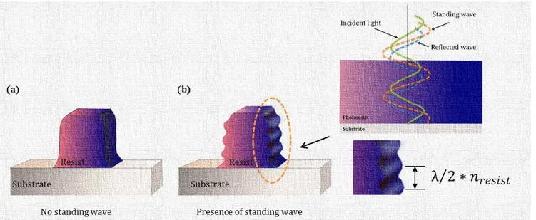
An important photoresist related aspect needs special attention: the reflectivity. A certain amount of incident light reaches the bottom part of the resist, thus the stack underneath. As the resist is partially reflective, this amount of light is reflected. Therefor interferences occur – constructive or destructive – between the incoming and reflected light. As consequence a periodic intensity distribution is introduced along the resist thickness that alters wavy the photoresist edges (see Figure 23). Thus it provides undulated resist profile after development that can have an important role on contrast10 degradation so as on pattern dimension.
10 Resist contrast: ~ corresponds to the remaining photoresist thickness after the development as a function of the
41
Figure 23: Illustration of a resist line after development that shows (a) no presence of standing wave (b) profile with standing wave
Several methods exist to minimize this swing curve profile effect such as the optimization of Post Exposure Bake (PEB) that induces the diffusion of the exposure generated compounds resulting in a smoothed out profile (due to the photoresist thermal reflow). The other option is the applications of Antireflective Layer Coating (ARC) to reduce the reflection, which can be introduced either on the top of the resist (TARC11) or either underneath (BARC12). Usually this
coated layer consists of a tenth to several hundreds of nanometer thickness of organic or non-organic material. Current technology applications rely on both solutions in fab.
1.3
The Lithographic Performance Indicators
The performance of photolithography, its constraints and the feasible strategies for further improvement are affected mainly by the following indicators of merit.
The Resolution 1.3.1
The limit of conventional projection optical lithography is defined by the resolution capability with an appropriate process control. The resolution of an optical system might be translated by the notion of the minimum printable feature size:
- If designed dimension on mask > minimum feature size : two separate points will remain separated after the aerial image diffraction into the photoresist;
11 Top Antireflective Coating : introduction of a thin film on top of the resist to reduce reflection from air-photoresist
interface and so to reduce undulated curves (caused by thin-film interference effects)
12 Bottom Antireflective Coating: introduction of an antireflective layer underneath the photoresist to reduce