HAL Id: hal-01722865
https://hal.archives-ouvertes.fr/hal-01722865
Submitted on 18 Jun 2019HAL is a multi-disciplinary open access archive for the deposit and dissemination of sci-entific research documents, whether they are pub-lished or not. The documents may come from teaching and research institutions in France or abroad, or from public or private research centers.
L’archive ouverte pluridisciplinaire HAL, est destinée au dépôt et à la diffusion de documents scientifiques de niveau recherche, publiés ou non, émanant des établissements d’enseignement et de recherche français ou étrangers, des laboratoires publics ou privés.
complex plasmonic nanostructures: spectra, maps and
radiation patterns from a generalized field propagator
Arnaud Arbouet, Adnen Mlayah, Christian Girard, Gérard Colas Des Francs
To cite this version:
Arnaud Arbouet, Adnen Mlayah, Christian Girard, Gérard Colas Des Francs. Electron energy losses and cathodoluminescence from complex plasmonic nanostructures: spectra, maps and radiation pat-terns from a generalized field propagator. New Journal of Physics, Institute of Physics: Open Access Journals, 2014, 16 (11), pp.113012. �10.1088/1367-2630/16/11/113012�. �hal-01722865�
PAPER • OPEN ACCESS
Electron energy losses and cathodoluminescence
from complex plasmonic nanostructures: spectra,
maps and radiation patterns from a generalized
field propagator
To cite this article: Arnaud Arbouet et al 2014 New J. Phys. 16 113012
View the article online for updates and enhancements.
Related content
Engineering metallic nanostructures for plasmonics and nanophotonics Nathan C Lindquist, Prashant Nagpal, Kevin M McPeak et al.
-Shaping and manipulation of light fields with bottom-up plasmonic structures C Girard, E Dujardin, G Baffou et al.
-Plasmonic nanoparticles: fabrication, simulation and experiments Manuel R Gonçalves
-Recent citations
pyGDM—A python toolkit for full-field electro-dynamical simulations and evolutionary optimization of nanostructures Peter R. Wiecha
-Nanoporous Metallic Networks: Fabrication, Optical Properties, and Applications
Racheli Ron et al
-Imaging of Plasmonic Eigen Modes in Gold Triangular Mesoplates by Near-Field Optical Microscopy
Keisuke Imaeda et al
-from complex plasmonic nanostructures: spectra,
maps and radiation patterns from a generalized
field
propagator
Arnaud Arbouet1, Adnen Mlayah1, Christian Girard1and Gérard Colas des Francs2
1CEMES, CNRS and Université de Toulouse, 29, rue Jeanne Marvig 31055 Toulouse Cedex 4,
France
2Laboratoire Interdisciplinaire Carnot de Bourgogne (ICB), UMR 6303 CNRS, Université de
Bourgogne, 9 Avenue Savary, BP 47870, 21078 Dijon Cedex, France E-mail:[email protected]
Received 13 June 2014, revised 17 August 2014 Accepted for publication 18 September 2014 Published 4 November 2014
New Journal of Physics 16 (2014) 113012
doi:10.1088/1367-2630/16/11/113012
Abstract
We present a unified framework for the description of the interaction of fast electrons with complex nanostructures based on the Green dyadic method. We show that the computation of a generalized field propagator yields the electron energy losses and cathodoluminescence of nano-objects of arbitrary morpholo-gies embedded in complex dielectric media. Spectra and maps for both pene-trating and non-penepene-trating electron trajectories are provided. This numerical approach can be extended to describe complex experiments involving fast electrons and optically excited nanostructures.
Keywords: electron energy loss spectroscopy, cathodoluminescence, plasmo-nics, nano-optics, EELS, surface plasmons, transmission electron microscopy
Content from this work may be used under the terms of theCreative Commons Attribution 3.0 licence. Any further distribution of this work must maintain attribution to the author(s) and the title of the work, journal citation and DOI.
1. Introduction
Energy losses from fast electrons have provided the first experimental evidence of surface plasmons (SP) in metallic films (Powell and Swan 1959) and nano-objects (Fujimoto et al 1967). Stimulated by both instrumental (monochromators, detectors) and methodological (signal deconvolution and processing) advances, electron energy loss spectroscopy (EELS) and cathodoluminescence (CL) have since demonstrated their unique potential in probing SPs of metallic nanostructures with nanometer spatial resolution (García de Abajo and Kociak2008a, Sigle et al2009, García de Abajo2010, García de Abajo and Kociak 2008b, Alber et al 2012, Carbone et al 2009, Sigle et al 2009, Geuquet and Henrard 2010, Howie 2009, Myroshnychenko et al 2012, Scholl et al 2012, Bosman et al 2013). Besides the superior spatial resolution compared to optical techniques, the ability of fast electrons to probe the dark SP modes and provide simultaneously accurate information on the morphology and environment of the investigated nano-objects has given a central role to electron spectroscopies in experimental nanoplasmonics. Today, these techniques are used to investigate nanostructures of increasing complexity in which the particle morphology, the substrate or the interparticle interactions strongly influence their optical response. In return, the interpretation of these sophisticated experiments has stimulated the development of several simulation techniques based on the boundary element method (BEM) (García de Abajo et al 2002, Hohenester and Trügler 2012) or discrete dipole approximation (DDA) (Geuquet and Henrard 2010), for instance. The connection of the electron energy loss probability with the local density of electromagnetic modes of metallic particles has been analyzed in detail (García de Abajo and Kociak 2008a, Hohenester et al 2009, Boudarham and Kociak 2012). Recent advances in combined electron/optical spectroscopy techniques such as electron energy gain spectroscopy demonstrated in ultrafast transmission electron microscopes (TEM) or surface plasmon three-dimensional (3D) imaging push forward the need and development of novel simulation techniques (Hohenester et al2009, Nicoletti et al 2013, Hörl et al 2013, Rivacoba and Zabala 2014, Park and Zewail 2014).
In this article, we extend the 3D Green dyadic method (3D-GDM) and show that several aspects of the interaction of fast electrons with nanostructures, namely electron energy losses and CL can be accurately described using a generalizedfield propagator. The GDM is a well-established technique and is particularly well-suited for the description of the optical properties of nanostructures of arbitrary geometries, either isolated or electromagnetically coupled to other nano-objects or located in the vicinity of planar interfaces (Girard and Dereux 1996, Tripathy et al2011). Besides the far-field and near-field optical properties, the GDM has been used to predict the temperature increase induced in plasmonic particles by an optical excitation (Baffou et al 2010), to describe scanning optical microscopy experiments (Teulle et al 2012) or to visualize the 3D charge distribution associated with surface plasmon excitations (Marty et al 2010). In this work, we extend the 3D-GDM to more complex scenarios involving fast electrons interacting with plasmonic nanostructures.
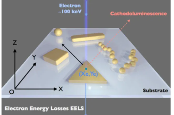
As depicted in figure 1, we first present the calculation of the energy losses of a fast electron impinging on a metallic nanostructure located on a substrate. The latter can be a simple homogeneous medium, but more complex cases, such as layered substrates, can also be considered. The electron is travelling along the (OZ) axis with a velocityv = −v ez and the substrate surface is the (OXY) plane. The metallic particle with permittivity εm( )ω is lying on
the substrate of dielectric constant εsub and is surrounded by a medium of dielectric constant
εenv.
The moving electron creates both charge and current distributions that can be written ρ( , )r t = −eδ(r− re( ))t and j r( , )t = −eδ(r− re( ))t v, respectively. These two spatio-temporal distributions are the sources of an electric field Eel( , )r t that can be derived from Maxwellʼs equations (Jackson 1998). In the( ,r ω) space, the Fourier components of Eel( , )r t can be written (in CGS units):
ω ω π γε γ ω γ ω γ = − − ω ⎡ + ⎣ ⎢ ⎛ ⎝ ⎜ ⎞ ⎠ ⎟ ⎛ ⎝ ⎜ ⎞ ⎠ ⎟ ⎤ ⎦ ⎥ e v i K R v K R v Eel( ,r ) 2 e ez eR , (1) env 0 1 z v i
where γ= 1 1 − εenvv c2 2 is the Lorentz contraction factor and cylindrical coordinates are used ( =r ReR+ z ez). For a 100 kV incident electron, v ≈ 0.5 and γ = 1.2. Kc 0 and K1 are
modified Bessel functions of the second kind. Rigorously, equation 1 should be modified to account for the electron interaction with interfaces between two different media. As detailed in the appendix, these corrections can be calculated from the boundary conditions and remain small outside of a thin layer above and below the interface. In the appendix, we show that their influence on the computed energy losses is weak. In the following, we have discarded these corrections to minimize the required computational ressources and used the bulk expression
ω
Eel( ,r ) in the EELS and CL simulations. Note that the electric field scattered by the nanostructures is calculated taking into account the substrate (see equations 10 and below). Only the incidentfield is approximated by its expression for an homogeneous medium (see also appendix). The contribution from Cherenkov radiation is not considered in the following.
2. Electron energy losses from a generalizedfield propagator
In this section, we show that it is possible to accurately compute the energy losses of a fast electron incident on any nanostructure from a generalized field propagator. The electric field associated with the electron induces a polarization distribution P r( , ω) inside the nanostructures. In turn, P r( ,ω) generates a secondary electric field Eind( ,r′ ω). The work accumulated by the electron against the Lorentz force decreases its kinetic energy by (García de
Figure 1. A fast electron incident along the (OZ) axis interacts with metallic nanostructures located on a dielectric substrate. The substrate plane is (OXY). The absolute (XYZ) frame is used to define the electron location.
Abajo 2010):
∫
ΔEEELS= e dt v E. ind(
re( ),t t)
(2)∫
Γ = +∞ E dE ( ),E (3) 0 EELSwhere ΓEELS( )E is the electron energy loss probability per unit energy (García de Abajo 2010):
∫
Γ ω = −∞ +∞ − ⎡⎣ ⎤⎦ (
)
E e t v E r t E ( ) 2 d Re . e( ), e Et . (4) EELS 2 ind iIn this equation, the Fourier component of the induced electric field Eind( ,r ω) can be calculated from the Green dyadic tensorS r r( , ′, ω) of the environment that connectsEind( ,r ω) to the polarization distributionP r( ,′ ω) (Martin et al 1995, Girard2005):
∫
ω = ′ ω ′ ω ′
E ( ,r ) S r r( , , ) · P r( , )dr , (5)
V
ind
where V is the volume of the nanostructure.
Assuming a local response of the metal, the electric susceptibility χ( ,r′ ω) can be defined as: χ ω ε ω ε π χ ω ′ = − ′ = ′ ∈ V r r r ( , ) ( ) 4 ( , ) 0 if elsewhere. (6) m env
Then, the Fourier componentsEind( ,r ω) of the induced electric field are:
∫
ω = ′ ′ ω χ ′ ω ′ ω
E ( ,r ) dr S r r( , , ) · ( ,r ) · E r( , ), (7)
V
ind
in whichE r( ,′ ω) is the self-consistent electric field in the nanostructure. This relation can be recast with a generalized propagator r r( , ′, ω) that directly connects the electricfield induced everywhere in the system to the electricfield of the probing electron itself:
∫
ω = ′ ′ ω ′ ω E ( ,r ) dr ( ,r r, ) · E ( ,r ) (8) V ind el ω ′ r r( , , ) is then given by:
ω χ ω ω
′ = ′ ′
( ,r r, ) ( ,r ) · ( ,r r, ), (9)
in which the Green dyadic tensor r r( , ′, ω) ensures self-consistency through:
∫
ω ω ω χ ω ω ′ = ′ + ″ ″ ″ ″ ′ r r S r r r S r r r r r ( , , ) ( , , ) d ( , , ) · ( , ) · ( , , ) (10) VThis Dyson equation can be solved by applying the numerical method described in (Martin et al1995) for electromagnetic scattering phenomena. The propagatorS r r( , ″, ω) is the sum of the vacuum propagatorS r r0( , ″, ω) and the surface propagatorSsurf( ,r r″, ω). For the latter, several options are available depending on the investigated situation (type of substrate, influence of retardation effects). In the most simple case, the non-retarded image dipole approximation yields a simple analytical expression ofSsurf( ,r r″, ω).
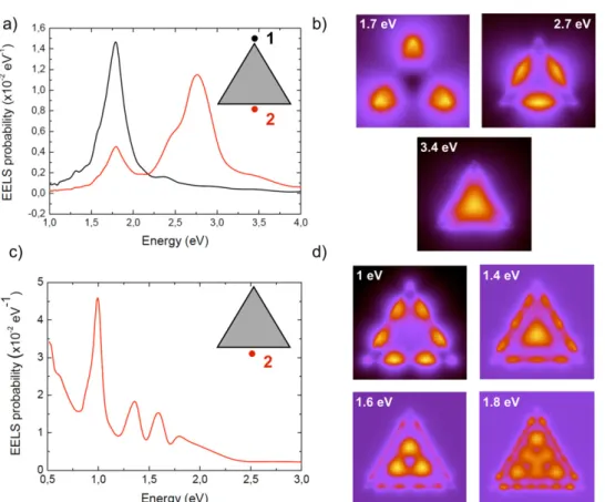
We first illustrate our method by considering a silver nanoprism located on a mica substrate as in (Nelayah et al 2007). In figure 2(a), we have computed the EELS of a 100 kV electron, 6 nm away from the apex of a gold nanoprism (position 1) or from the middle of an edge (position 2). The electron energy loss spectra display two clear features at 1.7 and 2.7 eV and a weaker shoulder around 3.4 eV. Infigure2(b), we have generated the EELS maps at these three energies. To do so, the position of the electron beam (Xelec, Yelec) is raster scanned over the nanoparticle, and the loss probability ΓEELS(Eloss) is computed at each position for afixed energy Eloss. The computed maps show that the enhanced electron energy losses at 2.7 and 1.7 eV are due to the excitation of quadrupolar and dipolar SP modes, respectively. These three features have been detected and ascribed to different surface plasmon modes (Nelayah et al 2007). The excellent agreement with these experiments shows that our method can accurately reproduce both spectra and spatial distributions recorded in EELS experiments (Nelayah et al2007).
As a second example, we now consider the interaction of fast electrons with a larger nanoprism. The gold nanoprism has an edge length of 950 nm and is located on a Si N3 4 substrate (figure2(c)). Similar nano-objects have been investigated by EELS, energy-filtered transmission electron microscopy (EFTEM) (Gu et al2011), two-photon photoluminescence (Viarbitskaya et al
Figure 2. (a) EELS spectra computed for a 100 kV electron incident at 6 nm from the apex (position 1) or middle of an edge (position 2) of a silver nanoprism (edge length a = 78 nm, thickness t = 10 nm) lying on a mica substrate (εsub= 2.3). (b) EELS maps computed at 1.7, 2.7 and 3.4 eV. (c) EELS spectra computed at 9 nm from a gold nanoprism edge (edge length a = 950 nm, thickness t = 15 nm lying on a Si N3 4substrate (εsub= 3.9). The electron kinetic energy is 200 keV. (d) EELS maps computed at 1, 1.4, 1.6 and 1.8 eV. The EELS probability is per electron and per unit energy.
2013) and dark-field microscopy (Major et al2013). The EELS spectrum is more complex and displays several features at 1, 1.4, 1.6 and 1.8 eV. We have mapped the electron energy loss probability at these four energies (figure2(d)). The EELS maps, in qualitative agreement with the experimental results of (Gu et al2011), confirm that the obtained features are due to high order SP modes. The latter are similar to the Fabry–Pérot optical cavity modes. With increasing energy, higher order plasmon modes are excited in the metallic resonator, and more nodes are visible. It is worth emphasizing that the inner structure of these modes has not been observed in the experiments most likely because of the large thickness of the investigated nano-objects, which strongly decreases the electron transmission (Gu et al2011).
3. Cathodoluminescence emission probability and radiation pattern from a generalized field propagator
In this part, we show that using the same generalized propagator r r( , ′, ω) of equation 9, another aspect of the interaction of fast electrons with nanostructures, namely, cathodolumi-nescence (CL), can be quantitatively reproduced. CL is widely used for the nanoscale exploration of the optical properties of semiconductor and metallic nanostructures (Zagonel et al 2010). It has recently been extended to measure in a scanning transmission electron microscope (STEM) the second order photon correlation of individual emitting centers in nanodiamonds (Tizei and Kociak 2013). The energy lost by an electron interacting with a metallic nanoparticle is either absorbed (and eventually converted into heat) or re-radiated in the far-field. In metallic nanostructures, the non-radiative inelastic decay channels are much faster than the radiative ones, and therefore light emission is dominated by electron-induced radiation emission; incoherent CL being much weaker (García de Abajo 2010). The coherent CL emission arises from the far-field radiation of the dipoles induced by the evanescent electric field associated with the moving charge. The total radiated energy ΔECL can be computed from theflux of the Poynting vector (Myroshnychenko et al 2012):
∫ ∫
Δ π Ω = ∧ E c t r d e E r t H r t 4 d ( ( , ) ( , )) (11) CL 2 r∫
ω ω∫
Γ Ω ω Ω = Ω +∞ d CL( , ) r d . (12) 0 2The number of photons emitted per electron, unit solid angle and unit energy ΓCL( ,Ω ω)is given by: Γ Ω ω = ω k E r ( , ) 1 ( , ) . (13) CL 2 rad 2
In the latter expression, Erad( ,r ω) is the Fourier transform of the total electric field radiated by the metallic nanostructure and k is the light wavevector in vacuum.Erad( ,r ω)can be computed from the polarization P r( ,′ ω) using the far-field asymptotic expression of the propagatorS∞( ,r r′, ω) (Novotny 1997):
∫
ω = ∞ ′ ω ′ ω ′ E ( ,r ) S ( ,r r, ) · P r( , )dr (14) V radThe polarization distribution is obtained from the induced electricfield using equations (1) and (8) and the susceptibility (6).
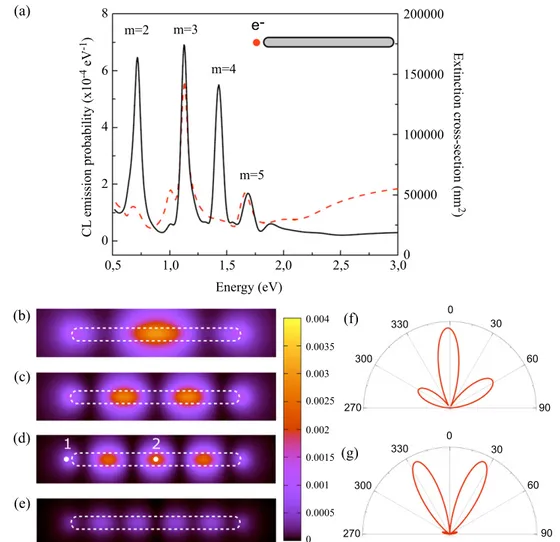
Figure 3(a) shows the CL spectrum collected using a mirror (NA = 0.8) placed above a gold nanowire located on a glass substrate. The electron probe passes 10 nm away from the nanowire end. Our calculations take into account the contribution from the glass substrate and the numerical aperture of the collecting mirror. Four features are clearly visible infigure3(a) at 0.72, 1.12, 1.42 and 1.69 eV. To shed light on their origin, we have plotted the CL photon emission intensity as a function of the electron beam position at each resonance energy. Figures 3(b)–(e) shows that the spatial distribution of the CL emission probability has a standing wave profile similar to Fabry–Pérot cavity modes. These modes are the counterpart of the high order multipolar surface plasmon modes, evidenced on the EELS maps offigure 2(d). They have already been observed in silver and gold nanowires (Vesseur et al 2007,
Gómez-m=2 m=3 m=4 m=5 8 6 4 2 0 0 0 0.0005 0.001 0.0015 0.002 0.0025 0.003 0.0035 0.004 50000 100000 150000 200000 0,5 1,0 1,5 2,0 2,5 3,0 Energy (eV) CL emission probability (x10 -4 eV -1) Extinction cross-section (nm 2 ) 270 270 300 300 330 330 0 0 30 30 60 60 90 90 e-(a) (c) (d) (e) (g) (f) (b)
Figure 3.CL photon emission spectrum excited by a 200 kV electron incident on a gold nanowire (length L = 700 nm, diameter D = 50 nm) lying on a substrate with εsub = 4 (solid line). The dashed line shows the extinction cross-section. The CL emission is collected by a mirror of numerical aperture NA = 0.8. The CL photon emission intensity is given per electron and per unit energy. (b–e) CL photon emission probability maps computed at 0.72, 1.12, 1.42 and 1.69 eV. (f) CL radiation pattern computed at 1.42 eV in a plane containing the nanowire for an electron incident at position 1 (see (d) map). (g) Same at position 2 (see (d) map).
Medina et al2008, Kuttge et al 2009) and gold ridges (Coenen et al2012). In our case, the SP resonances at 0.72, 1.12, 1.42 and 1.69 eV are ascribed respectively to the m = 2, 3, 4 and m = 5 surface plasmon resonances of the gold nanowire. A clear advantage of CL spectroscopy, besides its superior spatial resolution, is evidenced in figure 3(a) in which the extinction spectrum of the same nano-object is presented. Unless an asymmetric excitation (e.g. tilted beams) is used, optical spectroscopy techniques relying on plane-wave excitation are restricted to odd–order resonances (Dorfmüller et al2010). Figure3(a) clearly shows that the m = 2 and m = 4 resonances are not visible in the optical spectrum. The ability of CL spectroscopy to probe odd and even resonances is a consequence of the strong electricfield gradients associated with fast electrons. Furthermore, it has recently been shown that surface plasmon modes of even parity give rise to symmetric Lorentzian lineshapes, whereas modes of odd parity display asymmetric line profiles in the optical extinction spectrum of gold nanorods under near-normal plane-wave illumination (Verellen et al2014). The results offigure3(a) suggest that this effect also occurs in CL experiments.
Interestingly, relation (13) gives access to the angular distribution of the emitted CL which is another signature of the excited resonances. To illustrate this point we have calculated the angular distribution of the CL from the gold nanowire excited by an electron beam focused either near the end of the nanowire (position 1, figure 3(f)) or at its center (position 2, figure 3(g)) and at the energy of the m = 4 resonance. The radiation patterns presented in figures 3(f)–(g) are the result of the interferences of the radiation emitted by the polarization distribution generated in the nano-object. For instance,figure3(f) shows an asymmetric pattern because the electron excitation is shifted with respect to the center of the nanowire. Figure3(g) bears close ressemblance with the radiation pattern reported for gold ridges and for the same m = 4 resonance using angle-resolved cathodoluminescence experiments (Coenen et al2012).
4. Electron energy losses from nanostructures of arbitrary geometries in the presence of a substrate
The proposed method can also be applied to even more complex morphologies. To further illustrate this, we consider a randomly generated nanostructure consisting of 29 gold nanospheres (diameter D = 9 nm) partially or almost completely overlapping and located on a glass substrate (figure4(a)). Such a morphology mimicks the nanoporous metallicfilms recently investigated by combined STEM-EELS and high-angle annular dark-field microscopy (HAADF) (Bosman et al 2011, Losquin et al 2013). The latter studies have demonstrated that the peculiar optical properties of nanoporous metallic films originate from nanoscale variations of the number and spectral properties of the surface plasmon resonances supported by these complex objects with no clear correlation with their local morphology. Figures 4(b)–(d) shows the EELS probability maps computed at three different energies (1.5, 2 and 2.4 eV). As can be noticed, regions separated by few nanometers can have drastically different optical responses. Furthermore, as observed by (Bosman et al 2011), higher energy modes (2.4 eV) appear confined in smaller regions than lower energy modes (1.5 and 2 eV).
5. Conclusion
To summarize, we have presented a numerical framework that allows us to simulate, from a generalized propagator, the electron energy losses and CL caused by the interaction of a fast electron and a metallic nanostructure. This formalism accounts for both penetrating and non-penetrating trajectories, and nanostructures of arbitrary morphologies, and rigorously takes into account the environment. Its numerical implementation is fast and does not rely on numerical libraries. An extension of this approach would be adequate for the computation of the optical forces exerted on metallic nanoparticles or to more complex experiments such as electron energy gain spectroscopy experiments (García de Abajo and Kociak 2008b, Yurtsever et al 2012, Talebi et al 2013, Park and Zewail 2014).
Figure 4.(a) Randomly generated nanostructure composed of 29 gold spheres (diameter D = 9 nm). (b) EELS probability maps for a 200 kV electron incident computed at different energies. The substrate is glass (εsub = 2.25).
Acknowledgements
The authors acknowledge financial support from the European Union under the Seventh Framework Programme under a contract for an Integrated Infrastructure Initiative (Reference 312483 - ESTEEM2) and Agence Nationale de la Recherche (ANR, grant HYNNA ANR-10-BLAN-1016). This work was supported by the computing facility center CALMIP of the University Paul Sabatier of Toulouse (France). The authors thank N Renon for sharing his expertise in high-performance computing.
Appendix. Influence of a substrate on the electric field associated with a fast electron
We consider an electron traveling in a medium of dielectric constant ε2 with a velocity
= −v
v ez (v > 0) towards a substrate located in the z < 0 region and characterized by a dielectric constant ε1 (see figure 1). When the fast electron crosses the interface between two
media, expression 1 must be modified to take into account the influence of the charge distribution induced on the interface by the moving charge. It is possible to take into account these corrections by writing the electricfield in medium i as the sum of the electric field of the electron in an infinite bulk medium of dielectric constant εi, Eel,i( ,r ω) and the contribution from the surfaceEsurf,i( ,r ω):
ω = ω + ω
E ri( , ) Eel,i( ,r ) Esurf,i( ,r ) (A.1)
The electron electricfield in an infinite medium of dielectric constant ε1can be written as a
superposition of plane waves with transverse magnetic polarization:
∫ ∫
ω π ε = + − ε −ω − i e v q q k q k E r e ( , ) 2 e d d e . (A.2) i x y v c z i q q R el, 2 i 0 2 02 i . z v i //From the continuity of the parallel components of both E and B, it is possible to give the following expressions for the contribution from the surface Esurf,2( ,r ω) in the upper medium (z > 0 ):
∫
∫
∫
ω π ε π ω π ε π ω π ε π = − = − = − +∞ + +∞ + +∞ +(
)
(
)
(
)
i e vk q A q q q J q R x R i e vk q A q q q J q R y R i e vk q A q q J q R E r E r E r ( , ) 2 d e ( ) 2 i . ( , ) 2 d e ( ) 2 i . ( , ) 2 d e ( ) 2 . (A.3) q z z q z z q z surf,2,x 2 0 2 0 // i 2 ,2 // 2 1 // surf,2,y 2 0 2 0 // i 2 ,2 //2 1 // surf,2,z 2 0 2 0 // i 2 //3 0 // z z z ,2 ,2 ,2In the latter expressions, qz i, = − εik0 − q
2 //
2
, Jnare Bessel functions of the first kind of
order n and: ε ε ε ε β ε ε ε β ε = + + − − + − ⎡ ⎣ ⎢ ⎤ ⎦ ⎥ A q q q k q q k k q q k ( ) 1 (A.4) z z z z 2 2 ,1 1 ,2 1 0 2 ,1 2 2 02 2 0 2 ,1 2 1 02
Similarly, the contribution from the surface to the electricfield in the lower medium can be written:
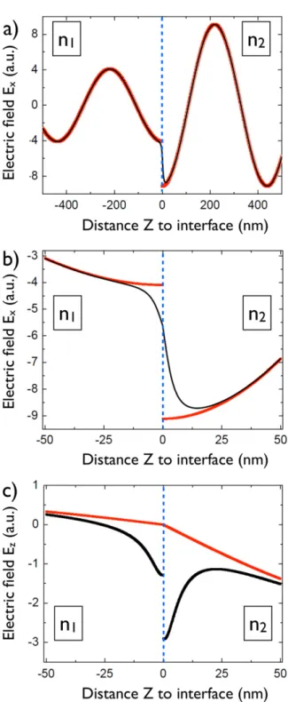
Figure A1. (a) X-component of the electric field associated with a 100 keV electron incident perpendicularly on a vacuum (n2)/SiO2(n1) interface calculated at 10 nm from
the electron trajectory. (b) Same in a small region around the interface. (c) Z-component of the electricfield associated with a 100 keV electron incident on vacuum (n2)/SiO2(n1)
∫
∫
∫
ω π ε π ω π ε π ω π ε π = = = − +∞ − +∞ − +∞ −(
)
(
)
(
)
i e vk q A q q q J q R x R i e vk q A q q q J q R y R i e vk q A q q J q R E r E r E r ( , ) 2 d e ( ) 2 i . ( , ) 2 d e ( ) 2 i . ( , ) 2 d e ( ) 2 . (A.5) q z z q z z q z 1 x 1 y 1 z surf, , 2 0 1 0 // i 1 ,1 // 2 1 // surf, , 2 0 1 0 // i 1 ,1 //2 1 // surf, , 2 0 1 0 // i 1 //3 0 // z z z ,1 ,1 ,1 With ε ε ε ε β ε ε ε β ε = + − − − − − ⎡ ⎣ ⎢ ⎤ ⎦ ⎥ A q q q k q q k k q q k ( ) 1 (A.6) z z z z 1 2 ,1 1 ,2 1 0 1 ,2 2 2 02 2 0 1 ,2 2 1 02In figure A1, we have computed the components along (OX) and (OZ) of both the total electricfieldE ri( ,ω) and the electricfield in the bulk Eel,i( ,r ω) in the two media above and below the interface. FiguresA1(a) and (b) show that taking into account the contribution from the surface Esurf,i( ,r ω) allows us to recover the continuity of the parallel electric field component. These results show that the influence of the interface contribution is weak outside of an≈50nm thick layer around the interface. It is furthermore possible to show that the relative importance of the corrections induced by the presence of the substrate is dependent upon the energy, as the low frequency Fourier components of the electricfield are more strongly affected away from the interface.
To go further, we have computed the electron energy losses using the method proposed above, taking into account either the bulk expressionEel,i( ,r ω)for the electricfield associated with the moving charge, or the corrected expressionE ri( , ω).
Figure A2.(Black squares) Electron energy losses of a 100 kV electron incident 12 nm away from a gold nanosphere (D = 10 nm) in vacuum computed with the bulk expressionEel,i( ,r ω). (Pink triangles) Same when the gold nanosphere is deposited on a vacuum/SiO2 interface computed with the total electricfield Ei( ,r ω). (Red dashed line) Electron energy losses experienced by a 100 kV electron incident on a bare vacuum/SiO2interface (data from (García de Abajo2010)).
These results of figure A2 show that the substrate-induced corrections to the incident E-field have a weak influence on the energy losses. This can be explained by the fact that the larger modification of the incident electric field induced by the interface contribution
ω
Esurf,i( ,r )is on the Z-component. On the contrary, along its trajectory, the electron probes the
electricfield radiated along the Z-component, which is radiated by dipoles oriented in-plane and is therefore not excited efficiently by the out-of-plane components of the electron electric field. Moreover, the nanosphere is only deposited on the vacuum/SiO2 interface, and therefore its dielectric environment is mainly vacuum, which explains that no observable redshift is evidenced.
References
Alber I, Sigle W, Demming-Janssen F, Neumann R, Trautmann C, van Aken P A and Toimil-Molares M E 2012 ACS Nano6 9711
Baffou G, Girard C and Quidant R 2010 Phys. Rev. Lett.104 136805
Bosman M, Anstis G R, Keast V J, Clarke J D and Cortie M B 2011 ACS Nano6 319
Bosman M, Ye E, Tan S F, Nijhuis C A, Yang J K W, Marty R, Mlayah A, Arbouet A, Girard C and Han M-Y 2013 Sci. Rep. 3 1312
Boudarham G and Kociak M 2012 Phys. Rev. B85 245447
Carbone F, Barwick B, Kwon O H, Park H S, Baskin J S and Zewail A H 2009 Chem. Phys. Lett.468 107 Coenen T, Vesseur E J R and Polman A 2012 ACS Nano6 1742
Dorfmüller J, Vogelgesang R, Khunsin W, Rockstuhl C, Etrich C and Kern K 2010 Nano Lett.10 3596 Fujimoto F, Komaki K-i and Ishida K 1967 J. Phys. Soc. Jpn.23 1186
García de Abajo F J and Kociak M 2008a Phys. Rev. Lett.100 106804 García de Abajo F J and Kociak M 2008b New J. Phys.10 073035 García de Abajo F J 2010 Rev. Mod. Phys.82 209
García de Abajo F J and Howie A 2002 Phys. Rev. B65 115418 Geuquet N and Henrard L 2010 Ultramicroscopy110 1075 Girard C and Dereux A 1996 Rep. Prog. Phys.59 657 Girard C 2005 Rep. Prog. Phys.68 1883
Gómez-Medina R, Yamamoto N, Nakano M and de Abajo F J G 2008 New J. Phys.10 105009
Gu L, Sigle W, Koch C T, Ögüt B, van Aken P A, Talebi N, Vogelgesang R, Mu J, Wen X and Mao J 2011 Phys. Rev. B83 195433
Hohenester U and Trügler A 2012 Computer Physics Communications183 370 Hohenester U, Ditlbacher H and Krenn J R 2009 Phys. Rev. Lett.103 106801 Hörl A, Trügler A and Hohenester U 2013 Phys. Rev. Lett.111 076801 Howie A 2009 Microscopy and Microanalysis15 314
Jackson J 1998 Classical Electrodynamics 3rd edn (New York: Wiley)
Kuttge M, Vesseur E J R, Koenderink A F, Lezec H J, Atwater H A, García de Abajo F J and Polman A 2009 Phys. Rev. B79 113405
Losquin A, Camelio S, Rossouw D, Besbes M, Pailloux F, Babonneau D, Botton G A, Greffet J-J, Stéphan O and Kociak M 2013 Phys. Rev. B88 115427
Major T A, Devadas M S, Lo S S and Hartland G V 2013 J. Phys. Chem. C117 1447 Martin O J F, Girard C and Dereux A 1995 Phys. Rev. Lett.74 526
Marty R, Baffou G, Arbouet A, Girard C and Quidant R 2010 Opt. Expr.18 3035 Myroshnychenko V et al 2012 Nano Lett.12 4172
Nelayah J, Kociak M, Stephan O, Garcia de Abajo F J, Tence M, Henrard L, Taverna D, Pastoriza-Santos I, Liz-Marzan L M and Colliex C 2007 Nat. Phys. 3 348
Nicoletti O, de la Pena F, Leary R K, Holland D J, Ducati C and Midgley P A 2013 Nature502 80 Novotny L 1997 J. Opt. Soc. Am. A14 105
Park S T and Zewail A H 2014 Phys. Rev. A89 013851 Powell C J and Swan J B 1959 Phys. Rev.115 869 Rivacoba A and Zabala N 2014 New J. Phys.16 073048 Scholl J A, Koh A L and Dionne J A 2012 Nature483 421
Sigle W, Nelayah J, Koch C T and van Aken P A 2009 Opt. Lett.34 2150 Talebi N, Sigle W, Vogelgesang R and van Aken New P 2013 J. Phys.15 053013
Teulle A, Marty R, Viarbitskaya S, Arbouet A, Dujardin E, Girard C and Colas des Francs G 2012 J. Opt. Soc. Am. B29 2431
Tizei L H G and Kociak M 2013 Phys. Rev. Lett.110 153604
Tripathy S, Marty R, Lin V K, Teo S L, Ye E, Arbouet A, Saviot L, Girard C, Han M Y and Mlayah A 2011 Nano Lett.11 431–7
Verellen N, López-Tejeira F, Paniagua-Domnguez R, Vercruysse D, Denkova D, Lagae L, van Dorpe P, Moshchalkov V V and Sánchez-Gil J A 2014 Nano Lett.14 2322
Vesseur E J R, de Waele R, Kuttge M and Polman A 2007 Nano Lett.7 2843
Viarbitskaya S, Teulle A, Marty R, Sharma J, Girard C, Arbouet A and Dujardin E 2013 Nat. Mater.12 426 Yurtsever A, van der Veen R M and Zewail A H 2012 Science335 59